
Related Manuals for Quectel EM05


Summary of Contents for Quectel EM05
- Page 1 EM05 Hardware Design LTE Module Series Rev. EM05_Hardware_Design_V1.0 Date: 2017-09-22 www.quectel.com...
- Page 2 QUECTEL OFFERS THE INFORMATION AS A SERVICE TO ITS CUSTOMERS. THE INFORMATION PROVIDED IS BASED UPON CUSTOMERS’ REQUIREMENTS. QUECTEL MAKES EVERY EFFORT TO ENSURE THE QUALITY OF THE INFORMATION IT MAKES AVAILABLE. QUECTEL DOES NOT MAKE ANY WARRANTY AS TO THE INFORMATION CONTAINED HEREIN, AND DOES NOT ACCEPT ANY LIABILITY FOR ANY INJURY, LOSS OR DAMAGE OF ANY KIND INCURRED BY USE OF OR RELIANCE UPON THE INFORMATION.
-
Page 3: About The Document
LTE Module Series EM05 Hardware Design About the Document History Revision Date Author Description Yeoman CHEN/ 2017-09-22 Initial Daryl DU EM05_Hardware_Design Confidential / Released 2 / 59... -
Page 4: Table Of Contents
LTE Module Series EM05 Hardware Design Contents About the Document ........................... 2 Contents ............................... 3 Table Index ..............................5 Figure Index ..............................6 Introduction ............................7 1.1. Safety Information........................8 Product Concept ..........................9 2.1. General Description ........................9 2.2. - Page 5 LTE Module Series EM05 Hardware Design 4.1. General Description ......................... 40 Antenna Interfaces ..........................41 5.1. Main/Rx-diversity Antenna Interfaces ..................41 5.2. GNSS Antenna Interface ......................42 5.3. Antenna Installation ......................... 42 5.3.1. Antenna Requirement ....................42 5.3.2. Recommended RF Connector for Antenna Installation ..........43 Electrical, Reliability and Radio Characteristics ................
- Page 6 LTE Module Series EM05 Hardware Design Table Index TABLE 1: FREQUENCY BANDS OF EM05 SERIES MODULE ................. 9 TABLE 2: KEY FEATURES OF EM05 ....................... 10 TABLE 3: DEFINITION OF I/O PARAMETERS ....................15 TABLE 4: DESCRIPTION OF PINS ........................15 TABLE 5: OVERVIEW OF OPERATING MODES .....................
- Page 7 FIGURE 30: CONNECTION BETWEEN THE RF CONNECTOR AND THE 1.13MM COAXIAL CABLE ..45 FIGURE 31: THERMAL DISSIPATION AREA ON BOTTOM SIDE OF THE MODULE ........53 FIGURE 32: MECHANICAL DIMENSIONS OF EM05 (UNIT: MM) ..............54 FIGURE 33: STANDARD DIMENSIONS OF M.2 TYPE 3042-S3 (UNIT: MM) ..........55 FIGURE 34: M.2 NOMENCLATURE .........................
-
Page 8: Introduction
This document can help customers to quickly understand the interface specifications, electrical and mechanical details, as well as other related information of EM05 module. To facilitate its application in different fields, reference design is also provided for customers’ reference. Associated with application note and user guide, customers can use the module to design and set up mobile applications easily. -
Page 9: Safety Information
EM05. Manufacturers of the cellular terminal should send the following safety information to users and operating personnel, and incorporate these guidelines into all manuals supplied with the product. If not so, Quectel assumes no liability for the customers’ failure to comply with these precautions. -
Page 10: Product Concept
It also provides optional GNSS functionality to meet customers’ specific application demands. EM05 contains three variants: EM05-CE, EM05-CML and EM05-E*. Customers can select a dedicated type based on the region or operator. The following table shows the frequency bands of EM05 series module. -
Page 11: Key Features
LTE Module Series EM05 Hardware Design 2.2. Key Features The following table describes the detailed features of EM05. Table 2: Key Features of EM05 Feature Details Function Interface PCI Express M.2 Standard Interface Supply voltage: 3.135V~4.4V Power Supply Typical supply voltage: 3.3V ... - Page 12 Rx-diversity Support LTE/WCDMA Rx-diversity Gen 8C Lite of Qualcomm GNSS Features Protocol: NMEA 0183 Compliant with 3GPP TS 27.007, 27.005 and Quectel enhanced AT AT Commands commands Size: (42± 0.15)mm × (30± 0.15)mm × (2.3+0.1/-0.2)mm Physical Characteristics Weight: approx. 6g Operation temperature range: -30°...
-
Page 13: Functional Diagram
LTE Module Series EM05 Hardware Design 2.3. Functional Diagram The following figure shows a block diagram of EM05. FULL_CARD_POWER_OFF# PMIC RESET# 19.2M Switch USB2.0 ANT_MAIN USIM Filter W_DISABLE1# LED# Baseband WOWWAN# ANT_GNSS Control Switch ANT_DIV NAND + DDR2 SDRAM Figure 1: Functional Diagram... -
Page 14: Application Interfaces
LTE Module Series EM05 Hardware Design Application Interfaces The physical connections and signal levels of EM05 comply with PCI Express M.2 specifications. This chapter mainly describes the definition and application of the following interfaces of EM05: Power supply ... -
Page 15: Pin Assignment
LTE Module Series EM05 Hardware Design 3.1. Pin Assignment The following figure shows the pin assignment of EM05. Pin Name Pin Name CONFIG_2 CONFIG_1 RESET# USIM_DET RESERVED RESERVED RESERVED RESERVED RESERVED Pin 75 Pin 74 RESERVED TX_BLANKING RESERVED GNSS_IRQ I2C_SDA... -
Page 16: Pin Description
LTE Module Series EM05 Hardware Design 3.2. Pin Description The following tables show the pin definition and description of EM05 on the 75-pin application. Table 3: Definition of I/O Parameters Type Description Bidirectional Digital input Digital output Open drain Power input... - Page 17 In slave mode, PCM_CLK 1.8V (AUDIO_0) it is an input signal. If unused, keep it open. Unconnected internally. CONFIG_0 CONFIG_0 EM05 is configured as WWAN-SSIC-0. GPIO_6 PCM_IN PCM data input 1.8V (AUDIO_1) A signal to wake up the host. GPIO_11 It is open drain and active low.
- Page 18 LTE Module Series EM05 Hardware Design GPIO_8- PCM data frame synchronization PCM_SYNC 1.8V AUDIO_3 signal SSIC-TxN UIM-RESET USIM_RESET Reset signal of (U)SIM card 1.8V/3.0V SSIC-TxP Clock signal of (U)SIM card UIM-CLK USIM_CLK 1.8V/3.0V clock Ground UIM-DATA USIM_DATA Data signal of (U)SIM card data 1.8V/3.0V...
- Page 19 USIM_DET (U)SIM card insertion detection 1.8V RESET# RESET# Reset the module. Active low. 1.8V SUSCLK (32kHz) Connected to GND internally. CONFIG_1 CONFIG_1 EM05 is configured as WWAN-SSIC-0. 3.3V Power supply 3.135V~4.4V Ground 3.3V Power supply 3.135V~4.4V Ground 3.3V Power supply 3.135V~4.4V...
-
Page 20: Operating Modes
Operating voltage (connected to VCC) remains applied. 3.4. Power Saving 3.4.1. Sleep Mode EM05 is able to reduce its current consumption to a minimum value during the sleep mode. The following section describes power saving procedure of EM05 module. EM05_Hardware_Design... -
Page 21: Usb Application With Usb Remote Wakeup Function
Sending data to EM05 through USB will wake up the module. When EM05 has a URC to report, the module will send remote wake-up signals via USB bus so as to wake up the host. 3.4.1.2. USB Application with USB Suspend/Resume and WOWWAN# Functions If the host supports USB suspend/resume, but does not support remote wake-up function, the WOWWAN# signal is needed to wake up the host. -
Page 22: Airplane Mode
Sending data to EM05 through USB will wake up the module. When EM05 has a URC to report, WOWWAN# signal will wake up the host. 3.4.2. Airplane Mode When the module enters into airplane mode, the RF function does not work, and all AT commands correlative with RF function will be inaccessible. -
Page 23: Power Supply
LTE Module Series EM05 Hardware Design 3.5. Power Supply The following table shows pin definition of VCC pins and ground pins. Table 6: Definition of VCC and GND Pins Pin No. Pin Name Power Domain Description 2, 4, 70, 72, 74 3.135V~4.4V... -
Page 24: Reference Design For Power Supply
LTE Module Series EM05 Hardware Design Module 220uF 100nF 10pF 33pF Figure 6: Reference Circuit of VCC 3.5.2. Reference Design for Power Supply Power design for the module is very important, as the performance of the module largely depends on the power source. -
Page 25: Monitor The Power Supply
EM05 can be turned on by driving the FUL_CARD_POWER_OFF# pin to a high level. It is recommended to use a GPIO from host to control the FUL_CARD_POWER_OFF#. A simple reference circuit is illustrated in the following figure. - Page 26 LTE Module Series EM05 Hardware Design A reference circuit is shown in the following figure. Module 1.8V/3.3V FUL_CARD_POWER_ OFF# Figure 9: Turn on the Module Automatically The turn on scenario is illustrated in the following figure. NOTE RESET_N ≥1.19V FUL_CARD_POWER_OFF# ≤0.2V...
-
Page 27: Turn Off The Module
LTE Module Series EM05 Hardware Design 3.6.2. Turn off the Module The following procedures can be used to turn off the module: Hardware shutdown: Turn off the module using the FUL_CARD_POWER_OFF# pin. Software shutdown: Turn off the module using AT+QPOWD command. -
Page 28: Reset The Module
LTE Module Series EM05 Hardware Design The power-down scenario is illustrated as the following figure. Log off from network in 3s POWERED DOWN AT+QPOWD <1s FUL_CARD_POWER_OFF# Module Power-down procedure RUNNING Status Figure 12: Timing of Turning off the Module Through AT Command During power-down procedure, the module will log off from network and save important data. - Page 29 LTE Module Series EM05 Hardware Design RESET# 4.7K Reset pulse Figure 13: Reference Circuit of RESET# by Using Driving Circuit RESET# Close to S2 Figure 14: Reference Circuit of RESET# by Using Button The reset scenario is illustrated in the following figure.
-
Page 30: U)Sim Interface
When (U)SIM card is absent, it is at low level. EM05 supports (U)SIM card hot-plug via the USIM_DET pin, which is a level trigger pin. The USIM_DET is normally short-circuited to ground when (U)SIM card is not inserted. When the (U)SIM card is inserted, the USIM_DET will change from low level to high level. - Page 31 LTE Module Series EM05 Hardware Design The following figure shows a reference design for normally short-circuited (U)SIM card connector. USIM_VDD 100nF (U)SIM Card Connector USIM_VDD USIM_RST Module USIM_CLK USIM_DET USIM_DATA 33pF 33pF 33pF Figure 16: Reference Circuit of Normally Short-Circuited (U)SIM Card Connector Normally Short-Circuited (U)SIM Card Connector ...
- Page 32 LTE Module Series EM05 Hardware Design Normally Open (U)SIM Card Connector When the (U)SIM is absent, CD is open to SW and USIM_DET is at low level. When the (U)SIM is inserted, CD is short-circuited to SW and USIM_DET is at high level.
-
Page 33: Usb Interface
USB_DM USB differential data bus (-) EM05 is compliant with USB 2.0 specification. It can only be used as a slave device. Meanwhile, it supports high speed (480Mbps) and full speed (12Mbps) mode. The USB interface is used for AT command communication, data transmission, GNSS NMEA output, software debugging and firmware upgrade. -
Page 34: Pcm And I2C Interfaces
128kHz PCM_CLK and an 8kHz, 50% duty cycle PCM_SYNC only. EM05 supports 8-bit A-law* and μ-law*, and also 16-bit linear data formats. The following figures show the primary mode’s timing relationship with 8kHz PCM_SYNC and 2048kHz PCM_CLK, as well as the auxiliary mode’s timing relationship with 8kHz PCM_SYNC and 128kHz PCM_CLK. - Page 35 LTE Module Series EM05 Hardware Design 125us PCM_CLK PCM_SYNC PCM_OUT PCM_IN Figure 21: Auxiliary Mode Timing The following table shows the pin definition of PCM and I2C interfaces which can be applied on audio codec design. Table 11: Pin Definition of PCM and I2C Interfaces Pin Name Pin No.
-
Page 36: Control And Indicator Signals
“*” means under development. It is recommended to reserve a RC (R=22Ω, C=22pF) circuit on the PCM lines, especially for PCM_CLK. EM05 works as a master device pertaining to I2C interface. EM05-CML does not support I2C interface. 3.11. Control and Indicator Signals The following table shows the pin definition of control and indicator signals. -
Page 37: W_Disable1# Signal
3.11.2. LED# Signal The LED# signal of EM05 is used to indicate the RF status of the module, which can absorb the current up to 40mA. According to the following circuit, in order to reduce the current of the LED, a resistor must be placed in series with the LED. -
Page 38: Wowwan# Signal
LTE Module Series EM05 Hardware Design Table 14: RF Status Indications of LED# Signal LED# Description Low Level (Light on) RF function is turned on RF function is turned off if any of the following circumstances occurs: The card is not powered High-impedance (Light off) ... -
Page 39: Dpr Signal
Figure 25: WOWWAN# Signal Reference Circuit Diagram 3.11.4. DPR Signal* EM05 provides an input pin DPR (Dynamic Power Reduction) for body SAR detection. The signal is sent by a host system proximity sensor to the wireless device to provide an input trigger which will reduce output power in the radio transmit. -
Page 40: Configuration Pins
LTE Module Series EM05 Hardware Design 3.12. Configuration Pins EM05 provides 4 configuration pins to configure the M.2 interface type, and it is configured as WWAN-SSIC 0 by default. Table 17: Pin Definition of Configuration Pins Pin No. Pin Name... -
Page 41: Gnss Receiver
EM05 supports standard NMEA-0183 protocol, and outputs NMEA sentences at 1Hz data update rate via USB interface by default. By default, EM05 GNSS engine is switched off. It has to be switched on via AT command. For more details about GNSS engine technology and configurations, please refer to document [3]. -
Page 42: Antenna Interfaces
EM05 Hardware Design Antenna Interfaces EM05 includes a main antenna interface, an Rx-diversity antenna interface which is used to resist the fall of signals caused by high speed movement and multipath effect, and a GNSS antenna interface. The antenna interfaces have an impedance of 50Ω. And the GNSS antenna interface is optional. -
Page 43: Gnss Antenna Interface
LTE Module Series EM05 Hardware Design 1880~1920 1880~1920 2300~2400 2300~2400 2555~2655 2555~2655 5.2. GNSS Antenna Interface The following table shows frequency specification of GNSS antenna interface. Table 20: GNSS Frequency Type Frequency Unit GPS/Galileo/QZSS 1575.42± 1.023 GLONASS 1597.5~1605.8 BeiDou 1561.098± 2.046 5.3. -
Page 44: Recommended Rf Connector For Antenna Installation
Cable insertion loss <2dB (LTE B38/B39/B40/B41) 5.3.2. Recommended RF Connector for Antenna Installation EM05 supports antenna connection via buckled RF connectors. Buckled RF connector MM4829-2702 supplied by MURATA or other equivalent connectors are recommended. The dimensions of MM4829-2702 connector are shown as below. - Page 45 Max 1.45 (3GHz~6GHz) The standard 2mm × 2mm RF receptacle connector to be used in conjunction with EM05 can be two types of mating plugs that meet a maximum height of 1.2mm using a Ø 0.81mm coax cable or a maximum height of 1.45mm utilizing a Ø...
- Page 46 LTE Module Series EM05 Hardware Design The following figure shows the specifications of 1.13mm coaxial cable mating the recommended RF connector. Figure 30: Connection between the RF Connector and the 1.13mm Coaxial Cable EM05_Hardware_Design Confidential / Released 45 / 59...
-
Page 47: Electrical, Reliability And Radio Characteristics
Peak Current of VCC Voltage at Digital Pins -0.3 6.2. Power Supply Requirements The input voltage of EM05 is 3.3V±5%, as specified by document [1]. The following table shows the power supply requirements of EM05. Table 24: Power Supply Requirements Parameter Description Min. -
Page 48: I/O Requirements
LTE Module Series EM05 Hardware Design 6.3. I/O Requirements Table 25: I/O Requirements Parameter Description Min. Max. Unit Input high voltage 0.7 × V +0.3 DD18 DD18 Input low voltage -0.3 0.3 × V DD18 Output high voltage -0.5 DD18... -
Page 49: Current Consumption
LTE Module Series EM05 Hardware Design 6.5. Current Consumption The values of current consumption are shown below. Table 27: EM05-CE Current Consumption Parameter Description Conditions Typ. Unit OFF state Power down AT+CFUN=0 WCDMA PF=64 WCDMA PF=128 WCDMA PF=256 Sleep state... - Page 50 WCDMA voice call WCDMA B8 @22.82dBm 550.0 BC0 Max Power @23.93dBm 598.0 CDMA voice call BC0 Min Power @-60.07dBm 123.0 Table 28: EM05-CML Current Consumption Parameter Description Conditions Typ. Unit OFF state Power down AT+CFUN=0 FDD-LTE PF=64 Sleep state FDD-LTE PF=128...
-
Page 51: Rf Output Power
LTE-TDD B40 @23dBm 430.0 (GNSS OFF) LTE-TDD B41 @23dBm 390.0 6.6. RF Output Power The following table shows the RF output power of EM05 module. Table 29: EM05 Conducted RF Output Power Frequency Max. Min. LTE-FDD Bands 23dBm± 2dB <-44dBm... -
Page 52: Rf Receiving Sensitivity
LTE Module Series EM05 Hardware Design 6.7. RF Receiving Sensitivity The following tables show conducted RF receiving sensitivity of EM05 series module. Table 30: EM05-CML Conducted RF Receiving Sensitivity Frequency Primary Diversity SIMO 3GPP (SIMO) LTE-TDD B38 (10M) -97.5dBm -99.0dBm -101.2dBm... -
Page 53: Esd Characteristics
Please add ground vias as many as possible on PCB for better heat dissipation. It is NOT recommended to apply solder mask on the main PCB below the thermal dissipation area of EM05, and the module should be kept away from heating sources. - Page 54 LTE Module Series EM05 Hardware Design The thermal dissipation area is shown as below. The dimensions are measured in mm. Thermal dissipation area Bottom View Figure 31: Thermal Dissipation Area on Bottom Side of the Module The table below shows the heat dissipation performance after adding a heat sink between the module and the main PCB.
-
Page 55: Mechanical Dimensions And Packaging
EM05 Hardware Design Mechanical Dimensions and Packaging This chapter mainly describes mechanical dimensions and packaging specifications of EM05 module. All dimensions are measured in mm, and the tolerances for dimensions without tolerance values are ± 0.05mm. 7.1. Mechanical Dimensions of the Module... -
Page 56: Standard Dimensions Of M.2 Pci Express
Figure 33: Standard Dimensions of M.2 Type 3042-S3 (Unit: mm) According to M.2 nomenclature, EM05 is Type 3042-S3-B (30.0mm × 42.0mm, max component height on the top is 1.5mm and single-sided, key ID is B). Figure 34: M.2 Nomenclature... -
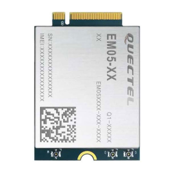
Page 57: Design Effect Drawings Of The Module
Figure 35: Top View of the Module Figure 36: Bottom View of the Module NOTE These are design effect drawings of EM05 module. For more accurate pictures, please refer to the module that you get from Quectel. EM05_Hardware_Design Confidential / Released... -
Page 58: Connector
EM05 adopts a standard PCI Express M.2 connector which compiles with the directives and standards listed in the document [1]. 7.5. Packaging The EM05 is packaged in tray. Each tray contains 10pcs of modules. The smallest package of EM05 contains 100pcs. EM05_Hardware_Design... -
Page 59: Appendix References
Document Name Remark PCI Express M.2 Specification PCI Express Specification Quectel_EM05_AT_Commands_Manual EM05 AT Commands Manual GNSS AT Commands Manual for EC25, Quectel_EC2x&EG9x&EM05_GNSS_AT_ EC21, EC20, EG95, EG91 and EM05 Commands_Manual modules Table 35: Terms and Abbreviations Abbreviation Description Bits Per Second DC-HSPA+... - Page 60 LTE Module Series EM05 Hardware Design HSUPA High Speed Uplink Packet Access kbps Kilo Bits Per Second Light Emitting Diode Long Term Evolution Mbps Million Bits Per Second Mobile Equipment (Module) MIMO Multiple-Input Multiple-Output MLCC Multiplayer Ceramic Chip Capacitor Multimedia Messaging Service...
Need help?
Do you have a question about the EM05 and is the answer not in the manual?
Questions and answers