
Related Manuals for Quectel RM510Q-GL


Summary of Contents for Quectel RM510Q-GL
- Page 1 RM510Q-GL Hardware Design 5G Module Series Version: 1.0 Date: 2021-03-25 Status: Released...
- Page 2 To the maximum extent permitted by law, Quectel excludes all liability for any loss or damage suffered in connection with the use of the functions and features under development, regardless of whether such loss or damage may have been foreseeable.
- Page 3 RM510Q-GL Hardware Design Copyright The information contained here is proprietary technical information of Quectel. Transmitting, reproducing, disseminating and editing this document as well as using the content without permission are forbidden. Offenders will be held liable for payment of damages. All rights are reserved in the event of a patent grant or registration of a utility model or design.
-
Page 4: Safety Information
Manufacturers of the cellular terminal should notify users and operating personnel of the following safety information by incorporating these guidelines into all manuals of the product. Otherwise, Quectel assumes no liability for customers’ failure to comply with these precautions. -
Page 5: About The Document
5G Module Series RM510Q-GL Hardware Design About the Document Revision History Version Date Author Description Kingson ZHANG 2020-10-22 Creation of the document /Jumping HE Kingson ZHANG 2021-03-25 First official release /Jumping HE RM510Q-GL_Hardware_Design 4 / 87... -
Page 6: Table Of Contents
5G Module Series RM510Q-GL Hardware Design Contents Safety Information ............................ 3 About the Document ..........................4 Contents ..............................5 Table Index ............................... 8 Figure Index ............................10 Introduction ............................. 11 1.1. Introduction ..........................11 1.2. Reference Standard ....................... 11 1.3. - Page 7 5G Module Series RM510Q-GL Hardware Design 4.3. PCIe Interface ........................42 4.3.1. PCIe Operating Mode ....................42 4.3.2. Pin Definition of PCIe ....................43 4.3.3. Reference Design of PCIe ................... 44 4.3.4. PCIe Timing ......................... 45 4.4. PCM Interface ........................46 4.5.
- Page 8 5G Module Series RM510Q-GL Hardware Design 6.3. Digital I/O Characteristic ......................77 6.4. Electrostatic Discharge ......................78 6.5. Absolute Maximum Ratings ....................79 6.6. Operating and Storage Temperatures ..................79 Mechanical Dimensions and Packaging ..................80 7.1. Mechanical Dimensions of the Module ................... 80 7.2.
- Page 9 RM510Q-GL Hardware Design Table Index Table 1: Special Marks ..........................12 Table 2: Frequency Bands and GNSS Type of RM510Q-GL Module ............. 13 Table 3: Key Features of RM510Q-GL ....................14 Table 4: Definition of I/O Parameters ...................... 20 Table 5: Pin Description .......................... 20 Table 6: Overview of Operating Modes ....................
- Page 10 5G Module Series RM510Q-GL Hardware Design Table 42: RM510Q-GL Current Consumption ..................72 Table 43: Logic Levels of Digital I/O (1.8 V) .................... 77 Table 44: (U)SIM 1.8 V I/O Requirements ....................78 Table 45: (U)SIM 3.0 V I/O Requirements ....................78 Table 46: Electrostatic Discharge Characteristics (Temperature: 25 º...
- Page 11 Figure 36: Install the Coaxial Cable Plug with A Jig ................71 Figure 37: Mechanical Dimensions of the Module (Unit: mm) ..............80 Figure 38: RM510Q-GL Top View and Bottom View ................81 Figure 39: Tray Size (Unit: mm) ......................82 Figure 40: Tray Packaging Procedure .....................
-
Page 12: Introduction
Coupled with application notes and user guides, you can easily design and set up mobile applications with RM510Q-GL. You can also view the reference design to understand hardware architecture of the module. For details, see document [1]. -
Page 13: Special Marks
5G Module Series RM510Q-GL Hardware Design 1.3. Special Marks Table 1: Special Marks Mark Definition Unless otherwise specified, when an asterisk (*) is used after a function, feature, interface, pin name, AT command, or argument, it indicates that the function, feature, interface, pin, AT command, or argument is under development and currently not supported;... -
Page 14: Product Concept
HSDPA, HSUPA and WCDMA networks. It is a standard M.2 Key-B WWAN module. For more details, see PCI Express M.2 Specification Revision 3.0, Version 1.2. RM510Q-GL is an industrial-grade module for industrial and commercial applications only. The module supports embedded operating systems such as Windows, Linux and Android, and also provide GNSS and voice functionality to meet specific application demands. -
Page 15: Key Features
⚫ Outdoor live devices ⚫ Wireless router and switch ⚫ Other wireless terminal devices 2.2. Key Features The following table describes key features of RM510Q-GL. Table 3: Key Features of RM510Q-GL Feature Details ⚫ Function Interface PCI Express M.2 Interface ⚫... - Page 16 5G Module Series RM510Q-GL Hardware Design ⚫ Used for audio function with external codec ⚫ Support 16-bit linear data format ⚫ PCM Interface Support long and short frame synchronization ⚫ Support master and slave modes, but must be the master in long frame synchronization ⚫...
- Page 17 5G Module Series RM510Q-GL Hardware Design WCDMA: 384 kbps (DL)/384 kbps (UL) ⚫ Rx-diversity Supports 5G NR/LTE/WCDMA Rx-diversity ⚫ Protocol: NMEA 0183 GNSS Features ⚫ Data Update Rate: 1 Hz ⚫ Antenna Interfaces ANT0, ANT1, ANT2, and ANT3_GNSSL1 ⚫ Compliant with 3GPP TS 27.007 and 3GPP TS 27.005 AT Commands ⚫...
-
Page 18: Evaluation Board
3GPP specifications again. 2.3. Evaluation Board To help you develop applications conveniently with the module, Quectel supplies an evaluation board (5G-mmWave-EVB), a USB micro-B cable, a USB type-C cable, antennas and other peripherals to control or test the module. -
Page 19: Functional Diagram
5G Module Series RM510Q-GL Hardware Design 2.4. Functional Diagram The following figure shows a block diagram of RM510Q-GL. ⚫ Power management ⚫ Baseband ⚫ LPDDR4X SDRAM + NAND Flash ⚫ Radio frequency ⚫ M.2 Key-B interface FULL_CARD_POWER_OFF# PMIC RESET# 38.4MHz XO... -
Page 20: Pin Assignment
5G Module Series RM510Q-GL Hardware Design 2.5. Pin Assignment The following figure shows the pin assignment of the module. The top side contains the antenna connectors. Pin Name Pin Name CONFIG_2 CONFIG_1 AP2SDX_STATUS RESET# PIN75 USIM1_DET PIN74 RFFE_VIO_1V8 COEX_TXD ANTCTL2... -
Page 21: Pin Description
5G Module Series RM510Q-GL Hardware Design 2.6. Pin Description Table 4: Definition of I/O Parameters Type Description Analog Input Analog Output Analog Input/Output Digital Input Digital Output Digital Input/Output Open Drain Power Input Power Output Pull Up Pull Down The following table shows the pin definition and description of the module. - Page 22 5G Module Series RM510Q-GL Hardware Design Ground Turn on/off the module. max = 4.4 V Internally pulled FULL_CARD_ High level: Turn on min = 1.19 V down with a 100 POWER_OFF# kΩ resistor. Low level: Turn off max = 0.2 V USB 2.0 differential data...
- Page 23 5G Module Series RM510Q-GL Hardware Design DIO, PCM_SYNC PCM data frame sync 1.8 V USB 3.1 super-speed USB_SS_TX_M transmit (-) USIM1_VDD USIM1_RST (U)SIM1 card reset 1.8/3.0 V USB 3.1 super-speed USB_SS_TX_P transmit (+) USIM1_VDD USIM1_CLK (U)SIM1 card clock 1.8/3.0 V...
- Page 24 5G Module Series RM510Q-GL Hardware Design Ground PCIe clock request. PCIE_CLKREQ_N Active LOW PCIE_REFCLK_M PCIe reference clock (-) PCIe wake up PCIE_WAKE_N Active LOW PCIE_REFCLK_P PCIe reference clock (+) Used for external MIPI IC RFFE_CLK* 1.8 V control Ground Used for external MIPI IC RFFE_DATA* 1.8 V...
- Page 25 CONFIG_2 Not connected internally NOTES If this function is required, please contact Quectel for more details. 、 This pin is pulled LOW by default, and will be internally pulled up to 1.8 V by software configuration only when (U)SIM hot-plug is enabled by AT+QSIMDET.
-
Page 26: Operating Characteristics
5G Module Series RM510Q-GL Hardware Design Operating Characteristics 3.1. Operating Modes The table below briefly summarizes the various operating modes to be mentioned in the following chapters. Table 6: Overview of Operating Modes Mode Details Software is active. The module has registered on the network, and it Idle is ready to send and receive data. -
Page 27: Sleep Mode
5G Module Series RM510Q-GL Hardware Design 3.1.1. Sleep Mode DRX of the module is able to reduce the current consumption to a minimum value during the sleep mode, and DRX cycle index values are broadcasted by the wireless network. The figure below shows the relationship between the DRX run time and the current consumption in sleep mode. -
Page 28: Airplane Mode
5G Module Series RM510Q-GL Hardware Design The module and the host will wake up in the following conditions: ⚫ Sending data to the module through USB will wake up the module. ⚫ When the module has a URC to report, it will send remote wake-up signals via USB bus to wake up the host. -
Page 29: Power Supply
5G Module Series RM510Q-GL Hardware Design RM510Q-GL can also be reprogrammed to PCIe mode based on eFuse. If the communication is switched to PCIe mode by burnt eFuse, the communication cannot be switched back to USB mode. Note that if the host does not support firmware upgrade through PCIe, the firmware can be upgraded by the PCIe Card EVB, which could be inserted into a PC. -
Page 30: Reference Design For Power Supply
5G Module Series RM510Q-GL Hardware Design In addition, to guarantee stability of the power supply, please use a zener diode with a reverse zener voltage of 5.1 V and a dissipation power of higher than 0.5 W. The following figure shows a reference circuit for the VCC. -
Page 31: Monitor The Power Supply
5G Module Series RM510Q-GL Hardware Design NOTE To avoid damages to the internal flash, DON'T cut off the power supply before the module is completely turned off by pulling down FULL_CARD_POWER_OFF# pin for more than 7 s, and DON'T cut off power supply directly when the module is working. - Page 32 5G Module Series RM510Q-GL Hardware Design It is recommended to use a host GPIO to control FULL_CARD_POWER_OFF#. A simple reference circuit is illustrated by the following figure. Host Module 1.8 V or 3.3 V FULL_CARD_POWER_OFF# GPIO PMIC 100k NOTE: The voltage of pin 6 should be no less than 1.19 V when it is at high level.
-
Page 33: Turn Off
5G Module Series RM510Q-GL Hardware Design 68 ms Module system turn-on time. turn-on 20 s 22 s Module system booting time. booting Network registering time related to network CSQ. registering 3.5. Turn off 3.5.1. Turn off the Module through FCPO# For the design that turns on the module with a host GPIO, when the power is supplied to VCC, driving FULL_CARD_POWER_OFF# pin LOW (≤... -
Page 34: Turn Off The Module Through At Command
5G Module Series RM510Q-GL Hardware Design 3.5.2. Turn off the Module through AT Command It is also a safe method to turn off the module by AT+QPOWD command. For more details about the command, see document [5]. The module is designed to be turned on with a host GPIO. Pull down FULL_CARD_POWER_OFF# pin after the module’s USB/PCIe is removed. - Page 35 5G Module Series RM510Q-GL Hardware Design Please note that triggering the RESET# signal will lead to loss of all data in the modem and removal of system drivers. It will also disconnect the modem from the network. Table 12: Definition of RESET# Pin Pin No.
- Page 36 5G Module Series RM510Q-GL Hardware Design The timing sequence of reset scenario is illustrated by the following figure. 3.7 V VCC(H) 1.5 V RESET# ≥ 1.19 V FCPO#(H) RST#-USIM 1.8 V RFFE_VIO_1V8 1.8 V or 3.0 V USIM_VDD Module Status...
-
Page 37: Application Interfaces
5G Module Series RM510Q-GL Hardware Design Application Interfaces The physical connections and signal levels of RM510Q-GL comply with PCI Express M.2 specification. This chapter mainly describes the definition and application of the following interfaces/pins of the module: ⚫ (U)SIM interfaces ⚫... -
Page 38: U)Sim Hot-Plug
5G Module Series RM510Q-GL Hardware Design NOTE This pin is pulled LOW by default, and will be internally pulled up to 1.8 V by software configuration only when (U)SIM hot-plug is enabled by AT+QSIMDET. 4.1.2. (U)SIM Hot-plug The module supports (U)SIM card hot-plug via the USIM1_DET pin. (U)SIM card insertion is detected by high/low level. -
Page 39: Normally Closed (U)Sim Card Connector
5G Module Series RM510Q-GL Hardware Design NOTES Hot-plug function is invalid if the configured value of <insert_level> is inconsistent with the hardware design. The underlined value is the default parameter value. USIM1_DET is pulled LOW by default, and will be internally pulled up to 1.8 V by software configuration only when (U)SIM hot-plug is enabled by AT+QSIMDET. -
Page 40: U)Sim Card Connector Without Hot-Plug
5G Module Series RM510Q-GL Hardware Design change from low to high level. ⚫ When the (U)SIM is absent, CD1 is open from CD2 and USIM1_DET is at high level. ⚫ When the (U)SIM is inserted, CD1 is pulled down to ground and USIM1_DET is at low level. -
Page 41: U)Sim Design Notices
5G Module Series RM510Q-GL Hardware Design 4.1.6. (U)SIM Design Notices To enhance the reliability and availability of the (U)SIM card in applications, please follow the criteria below in (U)SIM circuit design. ⚫ Place the (U)SIM card connector as close to the module as possible. Keep the trace length less than 200 mm. - Page 42 5G Module Series RM510Q-GL Hardware Design The USB 2.0 interface is recommended to be reserved for firmware upgrade in designs. The following figure shows a reference circuit of USB 3.1 & 2.0 interface. Host Module USB_SS_RX_P C3 220 nF USB_SS_TX_P...
-
Page 43: Pcie Interface
5G Module Series RM510Q-GL Hardware Design NOTES Only USB 2.0 can be used for firmware upgrade currently. 4.3. PCIe Interface The module provides one integrated PCIe (Peripheral Component Interconnect Express) interface. ⚫ PCI Express Base Specification Revision 3.0 compliant ⚫... -
Page 44: Pin Definition Of Pcie
5G Module Series RM510Q-GL Hardware Design NOTES The underlined value is the default parameter value. For more details about the command, see document [5]. 4.3.2. Pin Definition of PCIe Table 16: Pin Definition of PCIe Interface Pin No. Pin Name... -
Page 45: Reference Design Of Pcie
5G Module Series RM510Q-GL Hardware Design 4.3.3. Reference Design of PCIe The following figure shows a reference circuit for the PCIe interface. Host Module PCIE_REFCLK_P R4 0Ω PCIE_REFCLK_P R5 0Ω PCIE_REFCLK_M PCIE_REFCLK_M PCIE_RX_P C3 220 nF PCIE_TX_P PCIE_RX_M PCIE_TX_M C4 220 nF... -
Page 46: Pcie Timing
5G Module Series RM510Q-GL Hardware Design 4.3.4. PCIe Timing The following figure is PCIe power-up timing sequence for an adapter powered from system power rail in PCI Express M.2 specification. Figure 20: PCIe Power-up Timing Sequence of M.2 Specification The following table is power-up timing variables in PCI Express M.2 specification. -
Page 47: Pcm Interface
5G Module Series RM510Q-GL Hardware Design Table 18: PCIe Power-up Timing of the Module Symbol Min. Typ. Max. Comment 0 ms 20 ms Module power-on time depending on the host. power-on 68 ms Module system turn on time. turn-on 90 ms 100 ms PCIe clock request. - Page 48 5G Module Series RM510Q-GL Hardware Design 125 μs PCM_CLK PCM_SYNC PCM_DOUT PCM_DIN Figure 22: Primary Mode Timing Sequence 125 μs PCM_CLK PCM_SYNC PCM_DOUT PCM_DIN Figure 23: Auxiliary Mode Timing Sequence The following table shows the pin definition of PCM interface which can be applied to audio codec design.
-
Page 49: Control And Indication Interfaces
5G Module Series RM510Q-GL Hardware Design 4.5. Control and Indication Interfaces The following table shows the pin definition of control and indication pins. Table 20: Pin Definition of Control and Indication Interfaces Pin No. Pin Name Description DC Characteristics Airplane mode control. -
Page 50: W_Disable2
5G Module Series RM510Q-GL Hardware Design AT+CFUN=1 Low Level AT+CFUN=0 Disabled (no RF operation allowed) AT+CFUN=4 4.5.2. W_DISABLE2# The module provides a W_DISABLE2# pin to disable or enable the GNSS function. The W_DISABLE2# pin is pulled up by default. Driving it LOW will disable the GNSS function. The combination of W_DISABLE2# pin and AT commands can control the GNSS function. -
Page 51: Wwan_Led
5G Module Series RM510Q-GL Hardware Design 4.5.3. WWAN_LED# The WWAN_LED# signal is used to indicate RF status of the module, and its sink current is up to 10 mA. To reduce current consumption of the LED, a current-limited resistor must be placed in series with the LED, as illustrated by the figure below. -
Page 52: Dpr
5G Module Series RM510Q-GL Hardware Design Table 24: State of the WAKE_ON_WAN# WAKE_ON_WAN# State Module Operation Status Output a one-second low level pulse signal Call/SMS/Data is incoming (to wake up the host) Always at high level Idle/Sleep Host Module VCC_IO_HOST... -
Page 53: Status
5G Module Series RM510Q-GL Hardware Design 4.5.6. STATUS* The module provides two status indication pins for communication with IPQ807x device. Pin 38 (SDX2AP_STATUS) outputs the status indication signal to IPQ807x device, and pin 68 (AP2SDX_STATUS) inputs the status indication signal from IPQ807x device. -
Page 54: Configuration Pins
DO, PD Antenna Control GPIO 1.8 V NOTE If this function is required, please contact Quectel for more details. 4.8. Configuration Pins The module provides four configuration pins, which are defined as below. Table 28: Configuration Pins List of M.2 Specification... - Page 55 5G Module Series RM510Q-GL Hardware Design The following figure shows a reference circuit of these four pins. Host Module VCC_IO_HOST NM-0Ω CONFIG_0 GPIO 0Ω CONFIG_1 GPIO NM-0Ω CONFIG_2 GPIO CONFIG_3 NM-0Ω GPIO NOTE: The voltage level of VCC_IO_HOST depends on the host side and could be 1.8 V or 3.3 V.
-
Page 56: Rf Characteristics
5G Module Series RM510Q-GL Hardware Design RF Characteristics This chapter mainly describes RF characteristics of the module. 5.1. mmWave IF Interfaces 5.1.1. Pin Definition Eight mmWave IF interfaces are provided for the module’s supported FR2 (mmWave) bands n257, n258, n260, and n261. The following table lists the definition of these mmWave IF interfaces. -
Page 57: Port Mapping
5G Module Series RM510Q-GL Hardware Design 5.1.2. Port Mapping RM510Q-GL supports QTM525 (power class 3) and QTM527 (power class 1), and the IF port mapping is shown as below. Table 31: RM510Q-GL mmWave IF Port Mapping QTM_PON RM510Q-GL mmWave IF Port... -
Page 58: Port Mapping
5G Module Series RM510Q-GL Hardware Design LAA PRX WCDMA: LB_TRX Antenna 2 interface: 5G NR: LB_DRX & MHB_PRX MIMO & 600–5000 MHz; ANT2 n41 TRX0 & n77/n78/n79_TRX 50 Ω impedance LTE: LB_DRX & MHB_PRX MIMO & UHB_TRX WCDMA: LB_DRX Antenna 3 interface: 5G NR: MHB_DRX MIMO &... -
Page 59: Wcdma&Lte&5G Nr Characteristics
RM510Q-GL Hardware Design NOTES UHB frequency range: 3400–3800 MHz NR TRX1 = TX MIMO + PRX MIMO; NR DRX1 = DRX MIMO 5.2.3. WCDMA<E&5G NR Characteristics 5.2.3.1. Operating Frequency Table 34: RM510Q-GL Module Operating Frequency Transmit Band Name Receive (MHz) LTE-FDD LTE-TDD... -
Page 60: Receiving Sensitivity
1710–1780 2110–2200 663–698 617–652 3300–4200 3300–4200 3300–3800 3300–3800 4400–5000 4400–5000 5.2.3.2. Receiving Sensitivity The following tables show conducted receiving sensitivity of RM510Q-GL. Table 35: RM510Q-GL Conducted Receiving Sensitivity 3GPP Mode Frequency Primary Diversity SIMO (SIMO) WCDMA B1 -109.5 -110.3 -110.5... - Page 61 5G Module Series RM510Q-GL Hardware Design WCDMA B8 -109.5 -112 -111.5 -103.7 dBm WCDMA B19 -111 -112 -112 -104.7 dBm LTE-FDD B1 (10 MHz) -98.0 -99.2 -101.0 -96.3 dBm LTE-FDD B2 (10 MHz) -97.0 -99.2 -101.5 -94.3 dBm LTE-FDD B3 (10 MHz) -97.0...
- Page 62 5G Module Series RM510Q-GL Hardware Design LTE-TDD B42 (10 MHz) -96.8 -99.0 -100.5 -95 dBm LTE-TDD B43 (10 MHz) -96.8 -99.0 -100.5 -95 dBm LTE-TDD B48 (10 MHz) -96.8 -96.8 -99.0 -95 dBm LTE-FDD B66 (10 MHz) -96.8 -98.3 -100.2 -96.5 dBm...
-
Page 63: Output Power
5G Module Series RM510Q-GL Hardware Design 5G NR-TDD n78 (20 MHz) -86.0 -87.5 -89.0 -92.9 dBm (SCS: 30 kHz) 5G NR-TDD n79 (40 MHz) -86.0 -86.5 -89.5 -89.7 dBm (SCS: 30 kHz) NOTE SIMO is a smart antenna technology that uses a single antenna at the transmitter side and two antennas at the receiver side, which improves the Rx performance. -
Page 64: Gnss Frequency
Keep 15 dB isolation between each antenna to improve the receiving sensitivity. and 20 dB isolation between 5G NR UL MIMO TRX0 and TRX1 antennas. 5.2.4.2. GNSS Performance The following table shows GNSS performance of RM510Q-GL. Table 38: GNSS Performance Parameter Description Conditions Typ. -
Page 65: Sub-6&Gnss Antenna Requirements
5G Module Series RM510Q-GL Hardware Design Tracking Autonomous -159 Autonomous 33.99 Cold start @ open sky XTRA enabled 13.56 Autonomous 22.55 TTFF Warm start (GNSS) @ open sky XTRA enabled 2.02 Autonomous 1.33 Hot start @ open sky XTRA enabled 1.47... -
Page 66: Rf Connectors
5.3. RF Connectors 5.3.1. RF Connector Location RM510Q-GL has eight mmWave IF connectors (IFV4, IFH1, IFH2, IFV3, IFV2, IFH3, IFV1, and IFH4), three Sub-6 antenna connectors (ANT0, ANT1, and ANT2), and one Sub-6&GNSS antenna connector (ANT3_GNSSL1), which are shown as below. -
Page 67: Rf Connector Size
5G Module Series RM510Q-GL Hardware Design 5.3.2. RF Connector Size 5.3.2.1. mmWave IF Cable Connector The dimensions of antenna receptacle (IPEX: 20981-001E-02) on the RM510Q-GL and plug (IPEX: 20980-001R-13) are illustrated by the following figure. Figure 29: Dimensions of IF Connectors RM510Q-GL_Hardware_Design... -
Page 68: Sub-6&Gnss Antenna Connector
5G Module Series RM510Q-GL Hardware Design 5.3.2.2. Sub-6&GNSS Antenna Connector RM510Q-GL are mounted with standard 2 mm × 2 mm receptacle antenna connectors for convenient antenna connection. The antenna connector’s PN is IPEX 20579-001E, and the connector dimensions are illustrated as below:... -
Page 69: Recommended Rf Connector And Installation
5G Module Series RM510Q-GL Hardware Design 5.3.3. Recommended RF Connector and Installation The receptacle RF connector used in conjunction with the module will accept two types of mating plugs that will meet a maximum height of 1.2 mm using a Ø 0.81 mm coaxial cable or a maximum height of 1.45 mm utilizing a Ø... - Page 70 5G Module Series RM510Q-GL Hardware Design The following figure illustrates the connection between the receptacle RF connector on the module and the mating plug using a Ø 0.81 mm coaxial cable. Figure 32: Connection between RF Connector and Mating Plug Using Ø 0.81 mm Coaxial Cable The following figure illustrates the connection between the receptacle RF connector on the module and the mating plug using a Ø...
-
Page 71: Assemble Coaxial Cable Plug Manually
5G Module Series RM510Q-GL Hardware Design 5.3.3.1. Assemble Coaxial Cable Plug Manually The illustration for plugging in a coaxial cable plug is shown below, θ = 90° is acceptable, while θ ≠ 90° is not. Figure 34: Plug in the Coaxial Cable Plug The illustration of pulling out the coaxial cable plug is shown below, θ... -
Page 72: Assemble Coaxial Cable Plug With Jig
5G Module Series RM510Q-GL Hardware Design 5.3.3.2. Assemble Coaxial Cable Plug with Jig The pictures of installing the coaxial cable plug with a jig is shown below, θ = 90° is acceptable, while θ ≠ 90° is not. Figure 36: Install the Coaxial Cable Plug with A Jig 5.3.4. -
Page 73: Electrical Characteristics And Reliability
Typ. Max. Unit Power Supply 3.135 – Voltage Ripple – – Voltage Drop 6.2. Current Consumption Table 42: RM510Q-GL Current Consumption Description Conditions Typ. Unit μA OFF state Power off AT+CFUN=0 (USB suspend) 5.11 Sleep state WCDMA @ DRX = 0.64 s, USB suspend 5.389... - Page 74 5G Module Series RM510Q-GL Hardware Design LTE-TDD @ DRX = 0.64 s, USB suspend 5.803 WCDMA @ Paging Frame = 64 31.06 WCDMA @ Paging Frame = 64, USB active 52.42 LTE-FDD @ DRX = 0.64 s 32.93 Idle state LTE-FDD @ DRX = 0.64 s, USB active...
- Page 75 5G Module Series RM510Q-GL Hardware Design LTE-FDD B3 CH1575 @ 23 dBm LTE-FDD B4 CH2175 @ 23 dBm LTE-FDD B5 CH2525 @ 23 dBm LTE-FDD B7 CH3100 @ 23 dBm LTE-FDD B8 CH3625 @ 23 dBm LTE-FDD B12(B17) CH5095 @ 23 dBm...
- Page 76 5G Module Series RM510Q-GL Hardware Design 5G NR-TDD n41 CH501204 @ 26 dBm 5G NR-TDD n41 CH518598 @ 26 dBm 5G NR-TDD n41 CH535998 @ 26 dBm 5G NR-TDD n77 CH620668 @ 26 dBm 5G NR-TDD n77 CH650000 @ 26 dBm...
- Page 77 5G Module Series RM510Q-GL Hardware Design 5G NR-FDD n7 CH531000 @ 23 dBm 5G NR-FDD n7 CH537000 @ 23 dBm 5G NR-FDD n8 CH186000 @ 23 dBm 5G NR-FDD n8 CH188500 @ 23 dBm 5G NR-FDD n8 CH191000 @ 23 dBm...
-
Page 78: Digital I/O Characteristic
5G Module Series RM510Q-GL Hardware Design 5G NR-TDD n48 CH646333@ 23 dBm 5G NR-FDD n66 CH423000 @ 23 dBm 5G NR-FDD n66 CH429000 @ 23 dBm 5G NR-FDD n66 CH435000 @ 23 dBm 5G NR-FDD n71 CH124400 @ 23 dBm... -
Page 79: Electrostatic Discharge
5G Module Series RM510Q-GL Hardware Design Table 44: (U)SIM 1.8 V I/O Requirements Parameter Description Min. Max. Unit USIM1_VDD Power supply 1.65 1.95 Input high voltage 0.7 × USIM1_VDD USIM1_VDD + 0.3 Input low voltage -0.3 0.2 × USIM1_VDD Output high voltage 0.8 ×... -
Page 80: Absolute Maximum Ratings
5G Module Series RM510Q-GL Hardware Design 6.5. Absolute Maximum Ratings Absolute maximum ratings for power supply and voltage on digital and analog pins of the module are listed in the following table. Table 47: Absolute Maximum Ratings Parameter Min. Typ. -
Page 81: Mechanical Dimensions And Packaging
5G Module Series RM510Q-GL Hardware Design Mechanical Dimensions and Packaging This chapter mainly describes mechanical dimensions and packaging specifications of RM500Q-AE and RM502Q-AE. All dimensions are measured in mm, and the tolerances are ± 0.05 mm unless otherwise specified. 7.1. Mechanical Dimensions of the Module... -
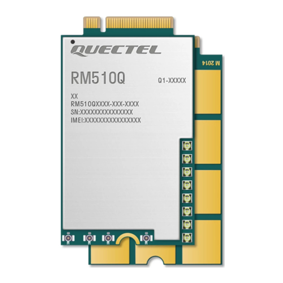
Page 82: Top And Bottom Views Of The Module
Images above are for illustration purpose only and may differ from the actual module. For authentic appearance and label, please refer to the module received from Quectel. If a conformal coating is necessary for the module, do NOT use any coating material that may chemically react with the PCB or shielding cover, and prevent the coating material from flowing into the module. -
Page 83: Packaging
5G Module Series RM510Q-GL Hardware Design 7.4. Packaging The modules are packaged in trays. The following figure shows the tray size. Figure 39: Tray Size (Unit: mm) Each tray contains 10 modules. The smallest package contains 100 modules. Tray packaging procedures are as below. - Page 84 5G Module Series RM510Q-GL Hardware Design Figure 40: Tray Packaging Procedure RM510Q-GL_Hardware_Design 83 / 87...
-
Page 85: Appendix References
5G Module Series RM510Q-GL Hardware Design Appendix References Table 49: Related Documents Document Name Description Quectel_RM510Q-GL_Reference_Design Reference Design for RM510Q-GL CA&EN-DC combinations of Quectel_RM510Q-GL_CA&EN-DC_Features RM510Q-GL RM510Q-GL mmWave EVB user Quectel_5G-mmWave_EVB_LP(525)_User_Guide guide (QTM525) RM510Q-GL mmWave EVB user Quectel_5G-mmWave_EVB_HP(527)_User_Guide guide (QTM527) Quectel_RG50xQ&RM5xxQ_Series_AT_Commands_... - Page 86 5G Module Series RM510Q-GL Hardware Design Dynamic Power Reduction Discontinuous Reception (Chapter 3.1.1, Chapter 6.2) Diversity Reception (Chapter 5) Electrostatic Discharge EndPoint Envelope tracking Frequency Division Duplexing Frequency Range 2 GLONASS Global Navigation Satellite System (Russia) GNSS Global Navigation Satellite System...
- Page 87 5G Module Series RM510Q-GL Hardware Design Mobile Originated Most Significant Bit Mobile Terminated Password Authentication Protocol Printed Circuit Board PCIe Peripheral Component Interconnect Express Pulse Code Modulation Protocol Data Unit Point-to-Point Protocol Radio Frequency RFFE RF Front-End RFIC Radio-frequency Integrated Circuit...
- Page 88 5G Module Series RM510Q-GL Hardware Design Input Low Voltage Level Output High Voltage Level Output Low Voltage Level VSWR Voltage Standing Wave Ratio WCDMA Wideband Code Division Multiple Access WLAN Wireless Local Area Network RM510Q-GL_Hardware_Design 87 / 87...
Need help?
Do you have a question about the RM510Q-GL and is the answer not in the manual?
Questions and answers