
Related Manuals for Quectel RM500Q-AE


Summary of Contents for Quectel RM500Q-AE
- Page 1 RM500Q-AE&RM502Q-AE Hardware Design 5G Module Series Version: 1.0.0 Date: 2020-10-22 Status: Preliminary www.quectel.com...
- Page 2 To the maximum extent permitted by law, Quectel excludes all liability for any loss or damage suffered in connection with the use of the functions and features under development, regardless of whether such loss or damage may have been foreseeable.
- Page 3 RM500Q-AE&RM502Q-AE Hardware Design Copyright The information contained here is proprietary technical information of Quectel wireless solutions co., ltd. Transmitting, reproducing, disseminating and editing this document as well as using the content without permission are forbidden. Offenders will be held liable for payment of damages. All rights are reserved in the event of a patent grant or registration of a utility model or design.
- Page 4 5G Module Series RM500Q-AE&RM502Q-AE Hardware Design About the Document Revision History Version Date Author Description Jared WANG 2020-10-22 Creation of the document /Hank LIU Jared WANG 1.0.0 2020-10-22 Preliminary /Hank LIU RM500Q-AE&RM502Q-AE_Hardware_Design 4 / 83...
-
Page 5: Table Of Contents
5G Module Series RM500Q-AE&RM502Q-AE Hardware Design Contents About the Document ..........................Contents ..............................Table Index ............................... Figure Index ............................1015 Introduction ............................ 1218 1.1. Safety Information ......................... 1319 Product Concept ..........................1420 2.1. General Description ......................1420 2.2. Key Features ......................... - Page 6 5G Module Series RM500Q-AE&RM502Q-AE Hardware Design GNSS Receiver ..........................5272 4.1. General Description ......................5272 4.2. GNSS Performance ......................5272 Antenna Interfaces ......................... 5474 5.1. RF Antenna Interfaces ......................5474 5.1.1. Antenna Pin Definition....................5474 5.1.2. RF Antenna Port Mapping ..................
- Page 7 5G Module Series RM500Q-AE&RM502Q-AE Hardware Design Table Index Table 1: Frequency Bands and GNSS Type of RM500Q-AE&RM502Q-AE Module ......1412 Table 2: Key Features of RM500Q-AE&RM502Q-AE ................1513 Table 3: Definition of I/O Parameters ..................... 2219 Table 4: Pin Description .........................
- Page 8 5G Module Series RM500Q-AE&RM502Q-AE Hardware Design 错误!未定义书签。错误!未定义书签。10 RM500Q-AERM500Q-AE&RM502Q-AE Module ....错误!超链接引用无效。Table 2: Key Features of RM500Q-AERM500Q-AE&RM502Q-AE .. 错误!未定义书 签。错误!未定义书签。11 错误!超链接引用无效。Table 3: Definition of I/O Parameters ..错误!未定义书签。错误!未定义书签。17 错误!超链接引用无效。Table 4: Pin Description ......错误!未定义书签。错误!未定义书签。17 错误!超链接引用无效。Table 5: Definition of VCC and GND Pins错误!未定义书签。错误!未定义书签。21...
- Page 9 5G Module Series RM500Q-AE&RM502Q-AE Hardware Design 错误!超链接引用无效。Table 32: I/O Requirements ....错误!未定义书签。错误!未定义书签。62 错误!超链接引用无效。Table 33: Operation and Storage Temperatures 错误!未定义书签。错误!未定义书 签。62 错误!超链接引用无效。Table 34: RM500Q-AERM500Q-AE&RM502Q-AE Current Consumption .. 错误!未 定义书签。错误!未定义书签。63 错误!超链接引用无效。Table 35: RF Output Power ..... 错误!未定义书签。错误!未定义书签。68 错误!超链接引用无效。Table 36: RM500Q-AERM500Q-AE&RM502Q-AE Conducted RF Receiving 错误!未定义书签。错误!未定义书签。68...
- Page 10 Figure 25: WAKE_ON_WAN# Signal Reference Circuit ................Figure 26: Recommended Circuit of Configuration Pins ................Figure 27: RM500Q-AE&RM502Q-AE Reference Circuit of RF Antenna ..........Figure 28: Microstrip Design on a 2-layer PCB ..................Figure 29: Coplanar Waveguide Design on a 2-layer PCB ...............
- Page 11 5G Module Series RM500Q-AE&RM502Q-AE Hardware Design Figure 42: Tray Size (Unit: mm) ......................... Figure 43: Tray Packaging Procedure ....................... RM500Q-AE&RM502Q-AE_Hardware_Design 11 / 83...
-
Page 12: Introduction
This document helps you quickly understand the interface specifications, electrical and mechanical details, as well as other related information of RM500Q-AE&RM502Q-AE. To facilitate its application in different fields, reference design is also provided for reference. Associated with application notes and user guides, customers can use the module to design and set up mobile applications easily. -
Page 13: Safety Information
Manufacturers of the cellular terminal should notify users and operating personnel of the following safety information by incorporating these guidelines into all manuals of the product. Otherwise, Quectel assumes no liability for customers’ failure to comply with these precautions. -
Page 14: Product Concept
Windows, Linux and Android, and also provides GNSS and voice functionality to meet specific application demands. The following table shows the frequency bands and GNSS type of the module. Table 1: Frequency Bands and GNSS Type of RM500Q-AE&RM502Q-AE Module Mode RM500Q-AE&RM502Q-AE 5G NR... -
Page 15: Key Features
5G Module Series RM500Q-AE&RM502Q-AE Hardware Design ⚫ Other wireless terminal devices 2.2. Key Features The following table describes key features of RM500Q-AE&RM502Q-AE. Table 2: Key Features of RM500Q-AE&RM502Q-AE Feature Details Function Interface PCI Express M.2 Interface ⚫ Supply voltage: 3.135–4.4 V Power Supply ⚫... - Page 16 Gen9 Lite of Qualcomm ⚫ GNSS Features Protocol: NMEA 0183 ⚫ Data Update Rate: 1 Hz ⚫ Compliant with 3GPP TS 27.007, 27.005 and Quectel enhanced AT AT Commands commands ⚫ Antenna Interfaces ANT0, ANT1, ANT2, and ANT3_GNSSL1 ⚫ Physical Size: (52.0 ±...
-
Page 17: Functional Diagram
5G Module Series RM500Q-AE&RM502Q-AE Hardware Design ⚫ Operating temperature range: -20 to +60 ° C ⚫ Restricted Operating temperature range: -30 to -20 ° C, +60 to +75 ° C Temperature Range ⚫ Extended temperature range: -40 to -30 ° C, +75 to +85 ° C ⚫... -
Page 18: Evaluation Board
2.3.2.4. Evaluation Board To help with the development of applications conveniently with RM500Q-AE&RM502Q-AE, Quectel supplies the evaluation board (PCIe Card EVB), a USB to RS-232 converter cable, a USB type-C cable, antennas and other peripherals to control or test the module. For more details, see document [1]. -
Page 19: Application Interfaces
5G Module Series RM500Q-AE&RM502Q-AE Hardware Design Application Interfaces The physical connections and signal levels of RM500Q-AE&RM502Q-AE comply with PCI Express M.2 specification. This chapter mainly describes the definition and application of the following interfaces/pins of the module: ⚫ Power supply ⚫... -
Page 20: Pin Assignment
5G Module Series RM500Q-AE&RM502Q-AE Hardware Design 3.1. Pin Assignment The following figure shows the pin assignment of the module. The top side contains module and antenna connectors. Pin Name Pin Name CONFIG_2 CONFIG_1 AP2SDX_STATUS RESET_N USIM_DET RFFE_VIO_1V8 COEX_TXD ANTCTL2 COEX_RXD... -
Page 21: Pin Description
5G Module Series RM500Q-AE&RM502Q-AE Hardware Design Pin Name Pin Name CONFIG_2 CONFIG_1 AP2SDX_STATUS RESET_N USIM_DET RFFE_VIO_1V8 COEX_TXD ANTCTL2 COEX_RXD PIN75 ANTCTL1 WLAN_TX_EN PIN74 LAA_TX_EN RFFE_DATA RFFE_CLK PCIE_REFCLK_P PCIE_WAKE_N PCIE_REFCLK_M PCIE_CLKREQ_N PCIE_RST_N PCIE_RX_P PCIE_RX_M PCIE_TX_P PCIE_TX_M SDX2AP_STATUS USB_SS_RX_P USIM_VDD USB_SS_RX_M USIM_DATA... - Page 22 5G Module Series RM500Q-AE&RM502Q-AE Hardware Design Table 3: Definition of I/O Parameters Type Description Analog Input Analog Output Digital Input Digital Output Bidirectional Open Drain Power Input Power Output The following table shows the pin definition and description of the module.
- Page 23 5G Module Series RM500Q-AE&RM502Q-AE Hardware Design Airplane mode control. W_DISABLE1#* 1.8/3.3 V power domain Active LOW. USB_DM USB 2.0 differential data (-) It is an open drain and WWAN_LED#* RF status indication LED active LOW signal. Ground Notch Notch Notch...
- Page 24 5G Module Series RM500Q-AE&RM502Q-AE Hardware Design USIM_CLK (U)SIM clock 1.8/3.0 V power domain Ground USIM_DATA (U)SIM card data 1.8/3.0 V power domain USB 3.1 super-speed USB_SS_RX_M receive (-) USIM_VDD (U)SIM card power supply 1.8/3.0 V power domain USB 3.1 super-speed...
- Page 25 5G Module Series RM500Q-AE&RM502Q-AE Hardware Design Used for external MIPI IC RFFE_CLK* 1.8 V power domain control Ground Used for external MIPI IC RFFE_DATA* 1.8 V power domain control Notification from SDR to LAA_TX_EN 1.8 V power domain WL when LTE transmitting...
-
Page 26: Operating Modes
5G Module Series RM500Q-AE&RM502Q-AE Hardware Design NOTE 1.Keep all NC, reserved and unused pins unconnected. 、 2.Pinpin 61/ and Ppin 63 isare used for ANTantenna tuner 3.3. Operating Modes The table below briefly summarizes the various operating modes to be mentioned in the following chapters. -
Page 27: Decrease Voltage Drop
5G Module Series RM500Q-AE&RM502Q-AE Hardware Design 2, 4, 70, 72, 74 3.135–4.4 V 3.7 V typical DC supply 3, 5, 11, 27, 33, 39, 45, 51, 57, Ground 71, 73 3.3.1.3.4.1. Decrease Voltage Drop The power supply range of the module is from 3.135 V to 4.4 V. Please ensure that the input voltage will never drop below 3.135 V, otherwise the module will be powered off automatically. -
Page 28: Reference Design For Power Supply
5G Module Series RM500Q-AE&RM502Q-AE Hardware Design Module 2, 4, 70, 72, 74 100 μF 1 μF 5.1 V 100 nF 33 pF 10 pF 3, 5, 11, 27, 33, 39, 45, 51, 57, 71, Figure 4: Reference Circuit of VCC Pins 3.3.2.3.4.2. -
Page 29: Turn On And Off Scenarios
5G Module Series RM500Q-AE&RM502Q-AE Hardware Design 3.4.3.5. Turn on and off Scenarios 3.4.1.3.5.1. Turn on the Module FULL_CARD_POWER_OFF# asynchronous signal is an Active Low input that is used to turn off the entire module. When the input signal is asserted high ( ≥ 1.19 the module will be enabled. -
Page 30: Turn Off The Module
5G Module Series RM500Q-AE&RM502Q-AE Hardware Design 3.4.1.1. Turn on the Module with a Host GPIO It is recommended to use a host GPIO to control FULL_CARD_POWER_OFF#. A simple reference circuit is illustrated in the following figure. Host Module 1.8 V or 3.3 V... -
Page 31: Turn Off The Module Through At Command
5G Module Series RM500Q-AE&RM502Q-AE Hardware Design The timing of turning-off scenario is illustrated in the following figure. RESET_N(H) FULL_CARD_POWER_OFF# ≥10 s Module Status RUNNING Power-off procedure Figure 8: Turn-off Timing through FULL_CARD_POWER_OFF# 3.4.2.2.3.5.2.2. Turn off the Module through AT Command It is also a safe way to use AT+QPOWD command to turn off the module. -
Page 32: Reset The Module
5G Module Series RM500Q-AE&RM502Q-AE Hardware Design NOTE Please pull down FULL_CARD_POWER_OFF# pin immediately or cut off the power supply VCC when the host detects that the module USB/PCIe is removed. 3.6. Reset the Module RESET_N is an asynchronous and active low signal (1.8 5... - Page 33 5G Module Series RM500Q-AE&RM502Q-AE Hardware Design Host Module VDD 1.5 V 100k RESET_N Reset pulse Reset Logic GPIO NMOS 200-700 ms 100k Figure 11: Reference Circuit of RESET_N with NMOS Driving Circuit VDD 1.5V 100k RESET_N Reset Logic 33 pF 200-700 ms The reset scenario is illustrated in the following figure.
- Page 34 NOTE “*” means under development. RM500Q-AE&RM502Q-AE supports (U)SIM card hot-plug via the USIM_DET pin. With a normally closed (U)SIM card connector, the USIM_DET is normally short-circuited to ground when a (U)SIM card is not inserted, and the USIM_DET will change from low to high voltage level when a (U)SIM card is inserted.
- Page 35 5G Module Series RM500Q-AE&RM502Q-AE Hardware Design USIM_VDD Module (U)SIM Card Connector 100 nF 10-20k USIM_VDD USIM_RST USIM_CLK USIM_DET USIM_DATA Note: All these resistors, capacitors and TVS should be close to (U)SIM card connector in PCB layout. Figure 13: Reference Circuit for Normally Closed (U)SIM Card Connector Normally Open (U)SIM Card Connector: ⚫...
-
Page 36: Usb Interface
(U)SIM card hot-plug is disabled by default. 3.6.3.8. USB Interface RM500Q-AE&RM502Q-AE module provides one integrated Universal Serial Bus (USB) interface which complies with the USB 3.1 & 2.0 specifications and supports super speed (10) on USB 3.1 and high RM500Q-AE&RM502Q-AE_Hardware_Design... - Page 37 5G Module Series RM500Q-AE&RM502Q-AE Hardware Design speed (480 Mbps) and full speed (12 Mbps) modes on USB 2.0. The USB interface is used for AT command communication, data transmission, GNSS NMEA sentence output, software debugging, firmware upgrade and voice over USB*.
- Page 38 5G Module Series RM500Q-AE&RM502Q-AE Hardware Design Host Module USB_SS_RX_P C5 220 nF USB_SS_TX_P USB_SS_RX_M C6 220 nF USB_SS_TX_M USB_SS_TX_P C1 220 nF USB_SS_RX_P USB_SS_TX_M C2 220 nF USB_SS_RX_M R1 0Ω USB_DM USB_DM R2 0Ω USB_DP USB_DP R3 NM-0Ω Test Points R4 NM-0Ω...
-
Page 39: Pcie Interface
Active LOW. 3.7.1.3.9.1. PCIe Operating Mode RM500Q-AE&RM502Q-AE supports endpoint (EP) mode and root complex (RC) mode. In EP mode, the module is configured as a PCIe EP device. In RC mode, the module is configured as a PCIe root complex. - Page 40 5G Module Series RM500Q-AE&RM502Q-AE Hardware Design Host Module PCIE_REFCLK_P PCIE_REFCLK_P PCIE_REFCLK_M PCIE_REFCLK_M PCIE_RX_P C5 220 nF PCIE_TX_P PCIE_RX_M C6 220 nF PCIE_TX_M PCIE_TX_P C1 220 nF PCIE_RX_P PCIE_TX_M C2 220 nF PCIE_RX_M VCC_IO_HOST 100k 100k 100k PCIE_WAKE_N PCIE_WAKE_N PCIE_CLKREQ_N PCIE_CLKREQ_N...
- Page 41 5G Module Series RM500Q-AE&RM502Q-AE Hardware Design Figure 18: PCIe Power-on Timing Requirements of M.2 Specification Module power-on or insertion detection power -on FUL L_CARD_ POWER_OFF System turn-on and booting 1.19 V 68 ms RESET_N turn-on RFFE_ VIO _1V8 23 ms...
-
Page 42: Usb And Pcie Modes
PCIe mode by burnt eFuse, the communication cannot be switched back to USB mode. Note that if the host does not support firmware upgrade through PCIe, then RM500Q-AE&RM502Q-AE USB 2.0 interface (Pin 7 and Pin 9) and two test points (VREG_L6E_1P8 and FORCE_USB_BOOT, RM500Q-AE&RM502Q-AE_Hardware_Design... -
Page 43: Pcm Interface
PCIe Card EVB, which could be inserted into a PC. For more details, see document [1]. 3.8.3.10. PCM Interface* RM500Q-AE&RM502Q-AE module supports audio communication via Pulse Code Modulation (PCM) digital interface. The PCM interface supports the following modes: ⚫... - Page 44 5G Module Series RM500Q-AE&RM502Q-AE Hardware Design 125 μs PCM_CLK PCM_SYNC PCM_DOUT PCM_DIN Figure 2122: Auxiliary Mode Timing The following table shows the pin definition of PCM interface which can be applied to audio codec design. Table 121211: Pin Definition of PCM Interface* Pin No.
-
Page 45: Control And Indication Interfaces
5G Module Series RM500Q-AE&RM502Q-AE Hardware Design 3.9.3.11. Control and Indication Interfaces The following table shows the pin definition of control and indication pins. Table 131312: Pin Definition of Control and Indication Interfaces Pin No. Pin Name Description Comment W_DISABLE1#* Airplane mode control. Active LOW. -
Page 46: W_Disable2
5G Module Series RM500Q-AE&RM502Q-AE Hardware Design Table 141413: RF Function Status W_DISABLE1# Level AT Commands RF Function Status High Level AT+CFUN=1 Enabled AT+CFUN=0 High Level Disabled AT+CFUN=4 AT+CFUN=0 Low Level AT+CFUN=1 Disabled AT+CFUN=4 3.9.2.3.11.2. W_DISABLE2#* RM500Q-AERM500Q-AE&RM502Q-AE module provides a W_DISABLE2# pin to disable or enable the GNSS function. -
Page 47: Wwan_Led
5G Module Series RM500Q-AE&RM502Q-AE Hardware Design Host Module VCC_IO_HOST VDD 1.8 V 100k 100k W_DISABLE2# GPIO W_DISABLE1# GPIO Note: The voltage level of VCC_IO_HOST could be 1.8 V or 3.3 V typically. Figure 22: W_DISABLE1# and W_DISABLE2# Reference Circuit 3.9.3. Figure 26: W_DISABLE1# and W_DISABLE2# Reference Circuit 3.9.4.3.11.3. -
Page 48: Wake_On_Wan
Note: The voltage level on VCC_IO_HOST depends on the host side due to the open drain in pin 23. Figure 24: WAKE_ON_WAN# Signal Reference Circuit 3.9.6.3.11.5. DPR* RM500Q-AE&RM502Q-AE module provides a DPR (Dynamic Power Reduction) pin for body SAR RM500Q-AE&RM502Q-AE_Hardware_Design 48 / 83... -
Page 49: Status
See document [2] for more details about AT+QCFG="sarcfg" command. 3.9.7.3.11.6. STATUS* RM500Q-AE&RM502Q-AE module provides two status indication pins for communication with IPQ807x device. Pin 38 (SDX2AP_STATUS) outputs the status indication signal to IPQ807x device, and pin 68 (AP2SDX_STATUS) inputs the status indication signal from IPQ807x device. -
Page 50: Antenna Tuner Control Interface
= 1.35 V ANTCTL2 max = 1.8 V NOTE “*” means under development. 3.12.3.14. Configuration Pins RM500Q-AE&RM502Q-AE module provides four configuration pins, which are defined as below. Table 21: Definition of Configuration Pins Pin No. Pin Name Power Domain Description CONFIG_0 Not connected internally RM500Q-AE&RM502Q-AE_Hardware_Design... - Page 51 5G Module Series RM500Q-AE&RM502Q-AE Hardware Design CONFIG_1 Connected to GND internally CONFIG_2 Not connected internally CONFIG_3 Not connected internally The following figure shows a reference circuit of these four pins. Host Module VCC_IO_HOST NM-0Ω CONFIG_0 GPIO 0Ω CONFIG_1 GPIO NM-0Ω...
-
Page 52: Gnss Receiver
GNSS Receiver 4.1. General Description RM500Q-AE&RM502Q-AE module includes a fully integrated global navigation satellite system solution that supports Gen9-Lite of Qualcomm (GPS, GLONASS, BeiDou/Compass, and Galileo). The module supports standard NMEA-0183 protocol, and outputs NMEA sentences at 1 Hz data update rate via USB interface by default. - Page 53 5G Module Series RM500Q-AE&RM502Q-AE Hardware Design Autonomous Hot start @ open sky XTRA enabled Accuracy Autonomous CEP-50 (GNSS) @ open sky NOTES Tracking sensitivity: the minimum GNSS signal power at which the module can maintain lock (keep positioning for at least 3 minutes continuously).
-
Page 54: Antenna Interfaces
5G Module Series RM500Q-AE&RM502Q-AE Hardware Design Antenna Interfaces RM500Q-AE&RM502Q-AE provides four antenna interfaces, the impedance of antenna port is 50 Ω. 5.1. RF Antenna Interfaces 5.1.1. Antenna Pin Definition The pin definition of RF antenna interfaces is shown below. Table 24: RM500Q-AE&RM502Q-AE Pin Definition of RF Antenna Interfaces... -
Page 55: Rf Antenna Port Mapping
UHB_DRX, GNSSL1 MIMO 2690 4200 LAA_DRx LTE UHB frequency range: 3400–5000 MHz. LTE UHB frequency range: 3400–5000 MHz. NOTE 5.1.3. Operating Frequency Table 26: RM500Q-AE&RM502Q-AE Module Operating Frequencies Transmit Receive Band Name LTE-FDD LTE-TDD UMTS 5G NR (MHz) (MHz) –... -
Page 56: Reference Design Of Rf Antenna Interface
A reference design of antenna interface is shown as below. A π-type matching circuit should be reserved for better RF performance. The capacitors are not mounted by default. Figure 26: RM500Q-AE&RM502Q-AE Reference Circuit of RF Antenna NOTES Keep the characteristic impedance for antenna trace as 50 Ω. -
Page 57: Gnss Antenna Interface
5G Module Series RM500Q-AE&RM502Q-AE Hardware Design 5.2. GNSS Antenna Interface The following table shows frequency specification of GNSS antenna connector. Table 272726: GNSS Frequency Type Frequency Unit GPS/Galileo/QZSS 1575.42 ± 1.023 (L1) Galileo 1575.42 ± 2.046 (E1) QZSS 1575.42 (L1) GLONASS 1597.5–1605.8... - Page 58 5G Module Series RM500Q-AE&RM502Q-AE Hardware Design Microstrip or coplanar waveguide is typically used in RF layout for characteristic impedance control. The following are reference designs of microstrip or coplanar waveguide with different PCB structures. Figure 27: Microstrip Design on a 2-layer PCB...
-
Page 59: Antenna Connectors
Keep RF traces away from interference sources, and avoid intersection and paralleling between traces on adjacent layers. For more details about RF layout, see document [4]. 5.4. Antenna Connectors RM500Q-AE&RM502Q-AE ANT0, ANT1, ANT2 and ANT3_GNSSL1 antenna connectors are shown as below. RM500Q-AE&RM502Q-AE_Hardware_Design 59 / 83... - Page 60 5G Module Series RM500Q-AE&RM502Q-AE Hardware Design ANT0 ANT1 ANT2 ANT3_GNSS Figure 31: RM500Q-AE Antenna Connectors ANT0 ANT1 ANT2 ANT3_GNSS Figure 32: RM502Q-AE Antenna Connectors RM500Q-AE&RM502Q-AE_Hardware_Design 60 / 83...
-
Page 61: Rf Bands Supported By Antenna Connectors
5G Module Series RM500Q-AE&RM502Q-AE Hardware Design 5.4.1 RF Bands Supported by Antenna Connectors Table 28: RF Bands Supported by RM500Q-AE&RM502Q-AE Antenna Connectors Description Frequency Name Antenna0 interface: 5G NR: ANT0 MHB_TRx & n41/n77/ _PRx MIMO; 1400–5000 MHz LTE: MHB_TRx & UHB_PRx MIMO... -
Page 62: Recommended Rf Connector For Antenna Installation
Cable insertion loss: < 2 dB LTE B7/B38/B41/B48 ⚫ 5G NR n7*/n41/n77 5.5.2. Recommended RF Connector for Antenna Installation RM500Q-AE&RM502Q-AE is mounted with standard 2 mm × 2 mm receptacle RF connectors for convenient antenna connection. RM500Q-AE&RM502Q-AE_Hardware_Design 62 / 83... - Page 63 5G Module Series RM500Q-AE&RM502Q-AE Hardware Design The connector dimensions are illustrated as below: Figure 3334: RM500Q-AE&RM502Q-AE RF Connector Dimensions (Unit: mm) Table 303029: Major Specifications of the RF Connector Item Specification Nominal Frequency Range DC to 6 GHz 50 Ω...
- Page 64 5G Module Series RM500Q-AE&RM502Q-AE Hardware Design Figure 3435: Specifications of Mating Plugs Using Ø0.81 mm Coaxial Cables The following figure illustrates the connection between the receptacle RF connector on the module and the mating plug using a Ø0.81 mm coaxial cable.
- Page 65 5G Module Series RM500Q-AE&RM502Q-AE Hardware Design Figure 36: Connection between RF Connector and Mating Plug Using Ø1.13 mm Coaxial Cable RM500Q-AE&RM502Q-AE_Hardware_Design 65 / 83...
-
Page 66: Reliability, Radio And Electrical Characteristics
5G Module Series RM500Q-AE&RM502Q-AE Hardware Design Reliability, Radio and Electrical Characteristics 6.1. Absolute Maximum Ratings Absolute maximum ratings for power supply and voltage on digital and analog pins of the module are listed in the following table. Table 31: Absolute Maximum Ratings Parameter Min. -
Page 67: I/O Requirements
5G Module Series RM500Q-AE&RM502Q-AE Hardware Design 6.3. I/O Requirements Table 33: I/O Requirements Parameter Description Min. Max. Unit Input high voltage 0.7 × V +0.3 DD18 DD18 Input low voltage -0.3 0.3 × V DD18 Output high voltage -0.5 DD18... -
Page 68: Current Consumption
, may undergo a reduction in value, exceeding the specified tolerances of 3GPP. When the temperature returns to the normal operating temperature level, the module will meet 3GPP specifications again. 6.5. Current Consumption Table 35: RM500Q-AE&RM502Q-AE Current Consumption Description Conditions Typ. - Page 69 5G Module Series RM500Q-AE&RM502Q-AE Hardware Design WCDMA B4 HSDPA CH1638 @ 23 dBm WCDMA B4 HSUPA CH1638 @ 23 dBm WCDMA B5 HSDPA CH4407 @ 23 dBm WCDMA B5 HSUPA CH4407 @ 23 dBm LTE-FDD B2 CH900 @ 23 dBm...
-
Page 70: Rf Output Power
5G Module Series RM500Q-AE&RM502Q-AE Hardware Design 5G NR-FDD n2 CH387000 @ 23 dBm 5G NR-FDD n2 CH392000 @ 23 dBm 5G NR-FDD n2 CH397000 @ 23 dBm 5G NR-FDD n5 CH174800 @ 23 dBm 5G NR-FDD n5 CH176300 @ 23 dBm... -
Page 71: Rf Receiving Sensitivity
For 5G NR TDD bands, the normative reference for this requirement is TS 38.101-1 [2] clause 6.3.1 6.7. RF Receiving Sensitivity The following tables show conducted RF receiving sensitivity of RM500Q-AE&RM502Q-AE. Table 37: RM500Q-AE&RM502Q-AE Conducted RF Receiving Sensitivity Mode Frequency... - Page 72 5G Module Series RM500Q-AE&RM502Q-AE Hardware Design LTE-FDD B13 (10 MHz) -93.3 dBm LTE-FDD B14 (10 MHz) -93.3 dBm LTE-FDD B17 (10 MHz) -93.3 dBm LTE-FDD B25 (10 MHz) -92.8 dBm LTE-FDD B26 (10 MHz) -93.8 dBm LTE-FDD B30 (10 MHz) -95.3 dBm...
-
Page 73: Esd Characteristics
± 1 6.9. Thermal Dissipation RM500Q-AE&RM502Q-AE is designed to work over an extended temperature range. In order to achieve a maximum performance while working under extended temperatures or extreme conditions (such as with maximum power or data rate) for a long time, it is strongly recommended to add a thermal pad or other thermally conductive compounds between the module and the main PCB for thermal dissipation. - Page 74 5G Module Series RM500Q-AE&RM502Q-AE Hardware Design Figure 37: Thermal Dissipation Area on Bottom Side of Module There are other measures to enhance heat dissipation performance: ⚫ Add ground vias as many as possible on PCB. ⚫ Maximize airflow over/around the module.
- Page 75 5G Module Series RM500Q-AE&RM502Q-AE Hardware Design react with the PCB or shielding cover, and prevent the coating material from flowing into the module. RM500Q-AE&RM502Q-AE_Hardware_Design 75 / 83...
-
Page 76: Mechanical Dimensions And Packaging
RM500Q-AE&RM502Q-AE. All dimensions are measured in mm, and the tolerances are ± 0.05 mm unless otherwise specified. 7.1. Mechanical Dimensions of the Module Figure 38: Mechanical Dimensions of the Module (Unit: mm) RM500Q-AE&RM502Q-AE_Hardware_Design 76 / 83... -
Page 77: Top And Bottom Views Of The Module
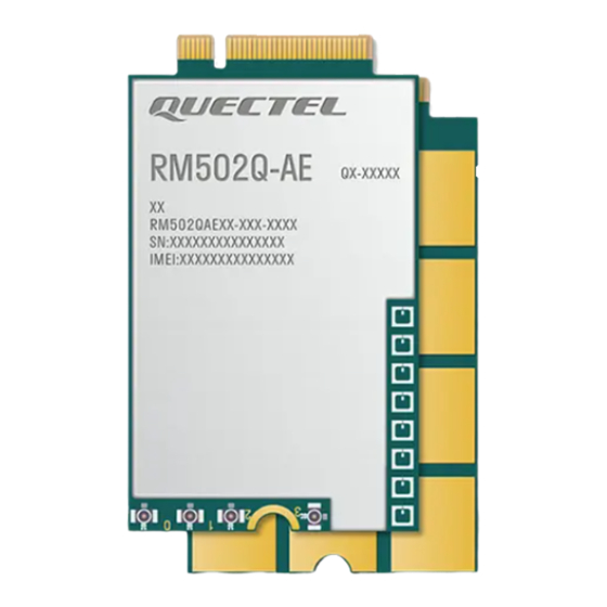
5G Module Series RM500Q-AE&RM502Q-AE Hardware Design 7.2. Top and Bottom Views of the Module Figure 3940: RM500Q-AE Top View and Bottom view Bottom View Top View Figure 4041: RM502Q-AE Top View and Bottom View RM500Q-AE&RM502Q-AE_Hardware_Design 77 / 83... -
Page 78: Connector
NOTE Images above are for illustration purpose only and may differ from the actual module. For authentic appearance and label, please refer to the module received from Quectel. 7.3. M.2 Connector The module adopts a standard PCI Express M.2 connector which compiles with the directives and standards listed in document [5]. - Page 79 5G Module Series RM500Q-AE&RM502Q-AE Hardware Design Figure 4243: Tray Packaging Procedure RM500Q-AE&RM502Q-AE_Hardware_Design 79 / 83...
-
Page 80: Appendix References
5G Module Series RM500Q-AE&RM502Q-AE Hardware Design Appendix References Table 39: Related Documents Document Name Remark Quectel_PCIe_Card_EVB_User_Guide PCIe card EVB user guide Quectel_RG50xQ&RM5xxQ_Series_AT_Commands_ AT commands manual for RG50xQ, Manual RM5xxQ series Quectel_RG50xQ&RM5xxQ_Series_GNSS_ The GNSS application note for Application_Note RG50xQ and RM5xxQ series... - Page 81 5G Module Series RM500Q-AE&RM502Q-AE Hardware Design Global System for Mobile Communications HSPA High Speed Packet Access HSUPA High Speed Uplink Packet Access kbps Kilo Bits Per Second License Assisted Access Light Emitting Diode Long Term Evolution Mbps Mega Bits Per Second...
- Page 82 5G Module Series RM500Q-AE&RM502Q-AE Hardware Design UART Universal Asynchronous Receiver & Transmitter Uplink Unsolicited Result Code Universal Serial Bus (U)SIM (Universal) Subscriber Identity Module Input High Voltage Level Input Low Voltage Level Output High Voltage Level Output Low Voltage Level...
- Page 83 FCC KDB996369 D03v01 Requirements List of applicable FCC rules FCC Part 15 Subpart B, Part 22 Subpart H, Part 24 Subpart E, Part 27 Subpart D & L & H & F & M & N, Part 90 Subpart R & S, Part 96 Summarize the specific operational use conditions Not Applicable Limited module procedures...
- Page 84 Label and compliance information Refer to FCC Label Information on test modes and additional testing requirements Not Applicable Additional testing, Part 15 Subpart B disclaimer Refer to FCC 15B Report...
- Page 85 FCC Certification Requirements. According to the definition of mobile and fixed device is described in Part 2.1091(b), this device is a mobile device. And the following conditions must be met: 1. This Modular Approval is limited to OEM installation for mobile and fixed applications only. The antenna installation and operating configurations of this transmitter, including any applicable source-based time-averaging duty factor, antenna gain and cable loss must satisfy MPE categorical Exclusion Requirements of 2.1091.
- Page 86 3.53 10.7 6.11 5. This module must not transmit simultaneously with any other antenna or transmitter 6. The host end product must include a user manual that clearly defines operating requirements and conditions that must be observed to ensure compliance with current FCC RF exposure guidelines.
- Page 87 uses and can radiate radio frequency energy and, if not installed and used in accordance with the instructions, may cause harmful interference to radio communications. However, there is no guarantee that interference will not occur in a particular installation. If this equipment does cause harmful interference to radio or television reception, which can be determined by turning the equipment off and on, the user is encouraged to try to correct the interference by one or more of the following measures:...
Need help?
Do you have a question about the RM500Q-AE and is the answer not in the manual?
Questions and answers