Sign In
Upload
Manuals
Brands
Intel Manuals
Motherboard
Arria 10 series
Intel Arria 10 series Manuals
Manuals and User Guides for Intel Arria 10 series. We have
3
Intel Arria 10 series manuals available for free PDF download: User Manual
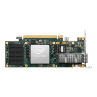
Intel Arria 10 series User Manual (607 pages)
Transceiver PHY
Brand:
Intel
| Category:
Transceiver
| Size: 4.99 MB
Table of Contents
User Guide
1
Table of Contents
2
1 Arria ® 10 Transceiver PHY Overview
8
Device Transceiver Layout
9
Arria 10 GX Device Transceiver Layout
10
Arria 10 GT Device Transceiver Layout
15
Arria 10 GX and GT Device Package Details
17
Arria 10 SX Device Transceiver Layout
17
Arria 10 SX Device Package Details
19
Transceiver PHY Architecture Overview
20
Transceiver Bank Architecture
20
PHY Layer Transceiver Components
25
Transceiver Phase-Locked Loops
28
Clock Generation Block (CGB)
29
Calibration
29
Intel Arria 10 Transceiver PHY Overview Revision History
30
2 Implementing Protocols in Arria 10 Transceivers
32
Transceiver Design IP Blocks
32
Transceiver Design Flow
33
Select and Instantiate the PHY IP Core
33
Configure the PHY IP Core
35
Generate the PHY IP Core
36
Select the PLL IP Core
36
Configure the PLL IP Core
38
Generate the PLL IP Core
39
Reset Controller
39
Create Reconfiguration Logic
39
Connect the PHY IP to the PLL IP Core and Reset Controller
40
Connect Datapath
40
Make Analog Parameter Settings
40
Compile the Design
41
Verify Design Functionality
41
Arria 10 Transceiver Protocols and PHY IP Support
41
Using the Arria 10 Transceiver Native PHY IP Core
45
Presets
48
General and Datapath Parameters
48
PMA Parameters
51
Enhanced PCS Parameters
55
Standard PCS Parameters
62
PCS Direct
67
Dynamic Reconfiguration Parameters
67
PMA Ports
73
Enhanced PCS Ports
76
Standard PCS Ports
86
IP Core File Locations
91
Unused Transceiver RX Channels
93
Unsupported Features
94
Interlaken
94
Metaframe Format and Framing Layer Control Word
95
Interlaken Configuration Clocking and Bonding
97
How to Implement Interlaken in Arria 10 Transceivers
103
Design Example
106
Native PHY IP Parameter Settings for Interlaken
107
Ethernet
111
Gigabit Ethernet (Gbe) and Gbe with IEEE 1588V2
112
10GBASE-R, 10GBASE-R with IEEE 1588V2, and 10GBASE-R with FEC
124
Variants
124
Transceiver Configurations
134
10GBASE-KR PHY IP Core
135
1-Gigabit/10-Gigabit Ethernet (Gbe) PHY IP Core
164
2.5G/5G/10G Multi-Rate Ethernet PHY IP Core
199
Release Information
200
Device Family Support
200
Configuration Registers
203
XAUI PHY IP Core
214
Xaui Phy Release Information
219
Xaui Phy Device Family Support
219
Parameterizing the Xaui Phy
221
Xaui Phy General Parameters
222
Xaui Phy Ports
222
Sdr Xgmii Tx Interface
224
Sdr Xgmii Rx Interface
224
Transceiver Serial Data Interface
224
Xaui Phy Pma Channel Controller Interface
225
Xaui Phy Optional Pma Control and Status Interface
225
Xaui Phy Register Interface and Register Descriptions
226
Acronyms
228
PCI Express (PIPE)
229
Transceiver Channel Datapath for PIPE
230
Supported PIPE Features
231
How to Connect TX Plls for PIPE Gen1, Gen2, and Gen3 Modes
240
How to Implement PCI Express (PIPE) in Arria 10 Transceivers
246
Native PHY IP Parameter Settings for PIPE
248
Fpll IP Parameter Core Settings for PIPE
253
ATX PLL IP Parameter Core Settings for PIPE
255
Native PHY IP Ports for PIPE
257
Fpll Ports for PIPE
264
ATX PLL Ports for PIPE
266
Preset Mappings to TX De-Emphasis
267
How to Place Channels for PIPE Configurations
268
PHY IP Core for Pcie (PIPE) Link Equalization for Gen3 Data Rate
274
Using Transceiver Toolkit (Ttk)/System Console/Reconfiguration Interface to Manually Tune Arria 10 Pcie Designs (Hard IP(HIP) and PIPE) (for Debug Only)
277
Cpri
279
Transceiver Channel Datapath and Clocking for CPRI
280
Supported Features for CPRI
281
Word Aligner in Manual Mode for CPRI
283
How to Implement CPRI in Arria 10 Transceivers
284
Native PHY IP Parameter Settings for CPRI
285
Other Protocols
289
Using the "Basic (Enhanced PCS)" and "Basic with KR FEC" Configurations of Enhanced PCS
289
Using the Basic/Custom, Basic/Custom with Rate Match Configurations of Standard PCS
300
Design Considerations for Implementing Arria 10 GT Channels
319
How to Implement PCS Direct Transceiver Configuration Rule
324
Simulating the Transceiver Native PHY IP Core
325
Nativelink Simulation Flow
326
Scripting IP Simulation
331
Custom Simulation Flow
332
Implementing Protocols in Intel Arria 10 Transceivers Revision History
335
3 Plls and Clock Networks
347
Plls
349
Transmit Plls Spacing Guideline When Using ATX Plls and Fplls
349
Atx Pll
350
Fpll
359
Cmu Pll
368
Input Reference Clock Sources
372
Dedicated Reference Clock Pins
374
Receiver Input Pins
374
PLL Cascading as an Input Reference Clock Source
375
Reference Clock Network
375
Global Clock or Core Clock as an Input Reference Clock
375
Transmitter Clock Network
375
X1 Clock Lines
376
X6 Clock Lines
377
Xn Clock Lines
379
GT Clock Lines
381
Clock Generation Block
383
FPGA Fabric-Transceiver Interface Clocking
384
Transmitter Data Path Interface Clocking
386
Receiver Data Path Interface Clocking
387
Unused/Idle Clock Line Requirements
389
Channel Bonding
389
PMA Bonding
389
PMA and PCS Bonding
391
Selecting Channel Bonding Schemes
392
Skew Calculations
393
PLL Feedback and Cascading Clock Network
393
Using Plls and Clock Networks
398
Non-Bonded Configurations
398
Bonded Configurations
403
Implementing PLL Cascading
408
MIX and Match Example
409
Timing Closure Recommendations
413
Plls and Clock Networks Revision History
414
4 Resetting Transceiver Channels
416
When Is Reset Required
416
Transceiver PHY Implementation
417
How Do I Reset
418
Model 1: Default Model
418
Model 2: Acknowledgment Model
427
Transceiver Blocks Affected by Reset and Powerdown Signals
432
Using the Transceiver PHY Reset Controller
433
Parameterizing the Transceiver PHY Reset Controller IP
435
Transceiver PHY Reset Controller Parameters
435
Transceiver PHY Reset Controller Interfaces
437
Transceiver PHY Reset Controller Resource Utilization
441
Using a User-Coded Reset Controller
441
User-Coded Reset Controller Signals
441
Combining Status or PLL Lock Signals
442
Timing Constraints for Bonded PCS and PMA Channels
443
Resetting Transceiver Channels Revision History
445
5 Arria 10 Transceiver PHY Architecture
447
Arria 10 PMA Architecture
447
Transmitter
447
Transmitter Buffer
448
Receiver
450
Receiver Buffer
451
Loopback
460
Arria 10 Enhanced PCS Architecture
461
Transmitter Datapath
462
Receiver Datapath
471
Arria 10 Standard PCS Architecture
479
Transmitter Datapath
480
Byte Serializer
481
Receiver Datapath
485
Byte Deserializer
493
Arria 10 PCI Express Gen3 PCS Architecture
495
Transmitter Datapath
496
Receiver Datapath
497
PIPE Interface
498
Intel Arria 10 Transceiver PHY Architecture Revision History
499
6 Reconfiguration Interface and Dynamic Reconfiguration
502
Reconfiguring Channel and PLL Blocks
503
Interacting with the Reconfiguration Interface
503
Reading from the Reconfiguration Interface
505
Writing to the Reconfiguration Interface
505
Configuration Files
506
Multiple Reconfiguration Profiles
509
Embedded Reconfiguration Streamer
510
Arbitration
512
Recommendations for Dynamic Reconfiguration
515
Steps to Perform Dynamic Reconfiguration
516
Direct Reconfiguration Flow
519
Native PHY IP or PLL IP Core Guided Reconfiguration Flow
519
Reconfiguration Flow for Special Cases
521
Switching Transmitter PLL
521
Switching Reference Clocks
523
Changing PMA Analog Parameters
527
Changing VOD, Pre-Emphasis Using Direct Reconfiguration Flow
530
Changing CTLE Settings in Manual Mode Using Direct Reconfiguration Flow
531
CTLE Settings in Triggered Adaptation Mode
531
Enabling and Disabling Loopback Modes Using Direct Reconfiguration Flow
533
Ports and Parameters
535
Dynamic Reconfiguration Interface Merging Across Multiple IP Blocks
542
Embedded Debug Features
544
Altera Debug Master Endpoint
544
Optional Reconfiguration Logic
544
Using Data Pattern Generators and Checkers
550
Using PRBS Data Pattern Generator and Checker
550
Using Pseudo Random Pattern Mode
559
Timing Closure Recommendations
560
Unsupported Features
563
Arria 10 Transceiver Register Map
564
Reconfiguration Interface and Dynamic Revision History
564
7 Calibration
567
Reconfiguration Interface and Arbitration with Presice Calibration Engine
567
Calibration Registers
569
Avalon-MM Interface Arbitration Registers
569
Transceiver Channel Calibration Registers
570
Fractional PLL Calibration Registers
570
ATX PLL Calibration Registers
571
Capability Registers
571
Rate Switch Flag Register
573
Power-Up Calibration
574
User Recalibration
576
Recalibration after Transceiver Reference Clock Frequency or Data Rate Change
579
Calibration Example
581
ATX PLL Recalibration
581
Fractional PLL Recalibration
581
CDR/CMU PLL Recalibration
582
PMA Recalibration
582
Calibration Revision History
583
8 Analog Parameter Settings
585
Making Analog Parameter Settings Using the Assignment Editor
585
Updating Quartus Settings File with the Known Assignment
585
Analog Parameter Settings List
586
Receiver General Analog Settings
588
Xcvr_A10_Rx_Link
588
Xcvr_A10_Rx_Term_Sel
589
Xcvr_Vccr_Vcct_Voltage - Rx
589
Receiver Analog Equalization Settings
590
CTLE Settings
590
VGA Settings
593
Decision Feedback Equalizer (DFE) Settings
594
Transmitter General Analog Settings
596
Xcvr_A10_Tx_Link
596
Xcvr_A10_Tx_Term_Sel
597
Xcvr_A10_Tx_Compensation_En
597
Xcvr_Vccr_Vcct_Voltage - Tx
598
Xcvr_A10_Tx_Slew_Rate_Ctrl
599
Transmitter Pre-Emphasis Analog Settings
600
Xcvr_A10_Tx_Pre_Emp_Sign_Pre_Tap_1T
600
Xcvr_A10_Tx_Pre_Emp_Sign_Pre_Tap_2T
600
Xcvr_A10_Tx_Pre_Emp_Sign_1St_Post_Tap
601
Xcvr_A10_Tx_Pre_Emp_Sign_2Nd_Post_Tap
601
Xcvr_A10_Tx_Pre_Emp_Switching_Ctrl_Pre_Tap_1T
602
Xcvr_A10_Tx_Pre_Emp_Switching_Ctrl_Pre_Tap_2T
602
Xcvr_A10_Tx_Pre_Emp_Switching_Ctrl_1St_Post_Tap
603
Xcvr_A10_Tx_Pre_Emp_Switching_Ctrl_2Nd_Post_Tap
604
Transmitter VOD Settings
604
Xcvr_A10_Tx_Vod_Output_Swing_Ctrl
604
Dedicated Reference Clock Settings
605
Xcvr_A10_Refclk_Term_Tristate
605
Xcvr_A10_Tx_Xtx_Path_Analog_Mode
606
Advertisement
Intel Arria 10 series User Manual (121 pages)
SoC Development Kit
Brand:
Intel
| Category:
Microcontrollers
| Size: 7.99 MB
Table of Contents
Table of Contents
2
1 Intel ® Arria ® 10 Soc Development Kit Overview
4
General Description
4
Board Component Blocks
6
Recommended Operating Conditions
8
Handling the Board
9
2 Getting Started
10
Board Inspection
10
Installing the Subscription Edition of the Quartus Prime Design Software
11
Activating Your License
12
Installing the Altera Soc Embedded Development Suite (EDS)
12
Development Kit Installer
13
Installing the USB-Blaster Driver
13
SD Card Image with Example Software
14
3 Development Board Setup
15
Applying Power to the Board
15
Default Switch and Jumper Settings
16
4 Board Test System
20
Preparing the Board
21
Running the Board Test System
22
Version Selector
22
Using the Board Test System
24
Using the Configure Menu
24
The System Info Tab
26
The GPIO Tab
27
The XCVR Tab
28
The Pcie Tab
30
The FMCA Tab
33
The FMCB Tab
36
The DDR3 Tab
40
The DDR4 Tab
42
The EEPROM Tab
43
The Power Monitor
44
The Clock Control
46
5 Board Components
48
Board Overview
48
Featured Device: Arria 10 Soc
51
MAX V CPLD 5M2210 System Controller
52
Configuration
60
System Controller Configuration
60
FPGA and I/O MUX CPLD Programming over On-Board USB-Blaster II
61
FPGA Programming by HPS
63
FPGA Programming by EPCQ Device
63
FPGA Programming over External USB-Blaster
63
Status Elements
64
Setup Elements
64
Board Settings DIP Switch
64
JTAG Chain Control DIP Switch
65
Reference Clock Source Selection
67
CPU Reset Push Button
67
Logic Reset Push Button
67
General User Input/Output
67
Character LCD
68
Clock Circuitry
69
On-Board Oscillators
69
Components and Interfaces
70
PCI Express
70
10/100/1000 Ethernet (HPS)
72
10/100/1000 Ethernet (FPGA)
74
Fmc
75
HPS Shared I/O
88
USB 2.0 Port (HPS)
90
Uart (Hps)
90
Real-Time Clock (HPS)
91
Sfp
91
I C Interface
92
FPGA General I/O Configuration
93
HPS SPIO Interface
100
Memory
105
FPGA External Memory
106
HPS External Memory
112
HPS Boot Flash Interface
115
C Eeprom
115
Daughtercards
116
Board Power Supply
117
Power Distribution System
118
Power Measurement
118
Additional Information
119
Document Revision History for the Intel Arria 10 Soc Development Kit User Guide
119
Compliance and Conformity Statements
121
CE EMI Conformity Caution
121
Intel Arria 10 series User Manual (43 pages)
FPGA HDMI Design Example
Brand:
Intel
| Category:
Motherboard
| Size: 0.38 MB
Table of Contents
Table of Contents
2
Arria ® 10 Devices
3
Directory Structure
3
1 Intel ® FPGA HDMI Design Example Quick Start Guide for Intel
4
Hardware and Software Requirements
7
Generating the Design
7
Simulating the Design
8
Compiling and Testing the Design
9
Design Limitation
10
Intel FPGA HDMI Design Example Parameters
10
2 Intel FPGA HDMI Design Example Detailed Description
11
HDMI RX-TX Retransmit Design Example
11
Design Components
13
Dynamic Range and Mastering (HDR) Infoframe Insertion and Filtering
20
Clocking Scheme
23
Interface Signals
26
Design RTL Parameters
36
Hardware Setup
37
Simulation Testbench
38
A Intel FPGA HDMI Design Example User Guide for Intel Arria 10 Devices Archives
41
B Revision History for Intel FPGA HDMI Design Example User Guide for Intel Arria 10 Devices
42
Advertisement
Advertisement
Related Products
Intel AN430TX - Motherboard - ATX
Intel AX965Q
Intel ATC6430M
Intel AR-B1760
Intel AP440FX
Intel AI5VG
Intel AL440LX
Intel Aero
Intel ATX586
Intel Arria 10 SDI II
Intel Categories
Motherboard
Computer Hardware
Server
Server Board
Desktop
More Intel Manuals
Login
Sign In
OR
Sign in with Facebook
Sign in with Google
Upload manual
Upload from disk
Upload from URL