
Related Manuals for Quectel SG368Z Series


Summary of Contents for Quectel SG368Z Series
- Page 1 SG368Z Series Hardware Design Smart Module Series Version: 1.0.0 Date: 2023-04-28 Status: Preliminary...
- Page 2 Smart Module Series At Quectel, our aim is to provide timely and comprehensive services to our customers. If you require any assistance, please contact our headquarters: Quectel Wireless Solutions Co., Ltd. Building 5, Shanghai Business Park Phase III (Area B), No.1016 Tianlin Road, Minhang District, Shanghai...
- Page 3 Privacy Policy To implement module functionality, certain device data are uploaded to Quectel’s or third-party’s servers, including carriers, chipset suppliers or customer-designated servers. Quectel, strictly abiding by the relevant laws and regulations, shall retain, use, disclose or otherwise process relevant data for the purpose of performing the service only or as permitted by applicable laws.
-
Page 4: Safety Information
Manufacturers of the cellular terminal should notify users and operating personnel of the following safety information by incorporating these guidelines into all manuals of the product. Quectel assumes no liability for customers’ failure to comply with these precautions. -
Page 5: About The Document
Smart Module Series About the Document Revision History Version Date Author Description Glenn GE/Jace ZHANG/ 2023-04-28 Creation of the document Szymon YU Glenn GE/Jace ZHANG/ 1.0.0 2023-04-28 Preliminary Szymon YU SG368Z_Series_Hardware_Design 4 / 113... -
Page 6: Table Of Contents
Smart Module Series Contents Safety Information ............................ 3 About the Document ..........................4 Contents ..............................5 Table Index ............................... 7 Figure Index .............................. 9 Introduction ............................. 11 1.1. Special Marks ........................11 Product Overview ..........................12 2.1. Frequency Bands and Functions ..................12 2.2. - Page 7 Smart Module Series 4.8.4. Audio Interfaces Design Considerations ..............54 4.9. ADC Interfaces ........................55 4.10. Video Output Interfaces ......................55 4.10.1. eDP Interface ......................56 4.10.2. HDMI Interface ..................... 58 4.10.3. LCM Interfaces ..................... 61 4.11. Camera Interface ........................63 4.11.1.
- Page 8 Smart Module Series Table Index Table 1: Special Marks ..........................11 Table 2: Basic Information ........................12 Table 3: Frequency Bands and Functions ....................12 Table 4: Key Features ..........................13 Table 5: Parameters Definition ........................ 18 Table 6: Pins Description ......................... 18 Table 7: VBAT and GND Pins ........................
- Page 9 Smart Module Series Table 42: Absolute Maximum Ratings ..................... 92 Table 43: Module’s Power Supply Ratings ....................92 Table 44: SG368Z-WF Power Consumption ................... 93 Table 45: SG368Z-AP Power Consumption .................... 94 Table 46: 1.8 V VCCIO I/O Characteristics (Unit: V) ................94 Table 47: PMUIO0 I/O Characteristics (Unit: V)..................
- Page 10 Smart Module Series Figure Index Figure 1: Functional Diagram ..............Error! Bookmark not defined. Figure 2: Pins Assignment (Top View) ..................... 17 Figure 3: Reference Design of Power Input .................... 34 Figure 4: Reference Design of Power Supply ..................35 Figure 5: Reference Design of Turn On with Driving Circuit ..............
- Page 11 Smart Module Series Figure 42: Top & Bottom Views of the Module ..................101 Figure 43: Recommended Reflow Soldering Thermal Profile ..............103 Figure 44: Carrier Tape Dimension Drawing ..................105 Figure 45: Plastic Reel Dimension Drawing ..................106 Figure 46: Mounting Direction ....................... 106 Figure 47: Packaging Process.......................
-
Page 12: Introduction
Smart Module Series Introduction This document describes the SG368Z series module’s features, performance, and air interfaces and hardware interfaces connected to your applications. The document provides a quick insight into interface specifications, RF performance, electrical and mechanical specifications, and other module information, as well. -
Page 13: Product Overview
Smart Module Series Product Overview SG368Z series is Quectel’s new generation of Linux/Android smart module. It is an SMD module with compact packaging and it supports built-in high performance ARM Mali G52 GPU, multiple audio and video codecs, and multiple audio and video input/output interfaces as well as abundant GPIO interfaces. -
Page 14: Key Features
Smart Module Series 5180–5825 MHz Bluetooth 4.2 2402–2480 MHz 2.2. Key Features Table 4: Key Features Categories Descriptions ⚫ Quad-core 64-bit ARM Cortex-A55 CPU Application Processor ⚫ Up to 2 GHz ⚫ 32 KB L1 I-cache, 32 KB L1 D-cache, 512 KB L3 cache ARM Mali G52 GPU Industrial grade: ⚫... - Page 15 Smart Module Series ⚫ Up to 8 groups of UART for SG368Z-WF; Up to 10 groups of UART for UART SG368Z-AP ⚫ Speed rate up to 4 Mbps ⚫ Up to 5 groups of I2C interfaces I2C Interfaces ⚫ Only support master mode ⚫...
-
Page 16: Functional Diagram
Smart Module Series ⚫ Wi-Fi & Bluetooth antenna interface (ANT_RF) Antenna Interface ⚫ 50 Ω characteristic impedance ⚫ Operating modes: AP and STA ⚫ Operating frequency: 2.4 GHz, 5 GHz WLAN Features ⚫ Protocol features: IEEE 802.11a/b/g/n/ac ⚫ Data rate: up to 433.3 Mbps ⚫... - Page 17 Smart Module Series NOTE SG368Z-AP does not support WLAN and Bluetooth function. SG368Z-WF only supports 1 group of RGMII interface. SG368Z_Series_Hardware_Design 16 / 113...
-
Page 18: Pins Assignment
Smart Module Series 2.4. Pins Assignment VCCIO6 RGMII1_TX1 RGMII1_RX_ RESERVED RGMII1_TX0 RGMII1_TX_ RGMII1_RX3 RGMII1_RX2 RGMII1_TX2 RGMII1_TX3 RGMII0_RX0 RGMII0_MDIO CAM0_PWDN CAM1_PWDN RGMII0_TX3 CAM0_RST CAM1_RST RGMII0_RX1 RGMII0_MDC RGMII0_RX_ GPIO3_C6 GPIO3_D0 RESERVED RGMII0_TX2 VCCIO4 RGMII0_ LCD1_RST GPIO3_D1 RGMII0_RX2 MCLK RESERVED GPIO2_C5 RGMII0_TX1 VCC_SPK_HP RGMII0_TX_ UART7_TXD RGMII0_RX3... -
Page 19: Pins Description
Smart Module Series 2.5. Pins Description Table 5: Parameters Definition Parameters Descriptions Analog Input Analog Output Analog Input/Output Digital Input Digital Output Digital Input/Output Open Drain Power Input Power Output DC characteristics include power domain and rate current in the table below. Table 6: Pins Description Power Supply Pin Name... - Page 20 Smart Module Series 1.8 V output power, reference voltage for VCCIO4 Vnom = 1.8 V VCCIO4 power domain 1.8 V output power, reference voltage for VCCIO5 Vnom = 1.8 V VCCIO5 power domain 1.8 V output power, reference voltage for VCCIO6 Vnom = 1.8 V VCCIO6 power...
- Page 21 Smart Module Series Headphone right HPH_R channel output Headphone If unused, connect HPH_GND reference ground this pin to ground. Loudspeaker output SPK_P Loudspeaker output SPK_M MIC_P Microphone input (+) MIC_M Microphone input (-) If the analog audio function is not Vmax = 5.5 V Analog audio power used, this pin...
- Page 22 Smart Module Series USB1 2.0 differential USB1_DM data (-) USB1 3.0 transmit USB1_SS_TX_P USB1 3.0 transmit USB1_SS_TX_M USB1_SS_RX_P USB1 3.0 receive (+) USB1_SS_RX_M USB1 3.0 receive (-) USB2 2.0 differential USB2_DP data (+) USB2 2.0 differential USB2_DM data (-) USB3 2.0 differential USB3_DP data (+) USB3 2.0 differential...
- Page 23 Smart Module Series PCIE2_RX0_P PCIe2 receive 0 (+) PCIE2_RX0_M PCIe2 receive 0 (-) PCIE2_RX1_P PCIe2 receive 1 (+) PCIE2_RX1_M PCIe2 receive 1 (-) PCIe2 reference If unused, connect PCIE2_REFCLK_P clock (+) this pin to ground. PCIe2 reference If unused, connect PCIE2_REFCLK_M clock (-) this pin to ground.
- Page 24 Smart Module Series SD_DATA1 SDIO data bit 1 VCCIO3 SD_DATA2 SDIO data bit 2 VCCIO3 SD_DATA3 SDIO data bit 3 VCCIO3 SD card hot-plug SD_DET PMUIO1 detect 1.8/3.3 V output Vnom = SD_PU_VDD power for SD card 1.8/3.3 V pull-up circuits Touch Panel Interface Pin Name Pin No.
- Page 25 Smart Module Series LCD0 MIPI lane 3 DSI0_LN3_P data (+) DSI1_CLK_N LCD1 MIPI clock (-) DSI1_CLK_P LCD1 MIPI clock (+) LCD1 MIPI lane 0 DSI1_LN0_N data (-) LCD1 MIPI lane 0 DSI1_LN0_P data (+) LCD1 MIPI lane 1 DSI1_LN1_N data (-) LCD1 MIPI lane 1 DSI1_LN1_P data (+)
- Page 26 Smart Module Series HDMI Interface Pin Name Pin No. Description Comment Characteristics HDMI_TX2_P HDMI data 2 (+) HDMI_TX2_M HDMI data 2 (-) HDMI_TX1_P HDMI data 1 (+) HDMI_TX1_M HDMI data 1 (-) HDMI_TX0_P HDMI data 0 (+) HDMI_TX0_M HDMI data 0 (-) HDMI_CLK_P HDMI clock (+) HDMI_CLK_M...
- Page 27 Smart Module Series MIPI CSI lane 2 data CSI_LN2_P MIPI CSI lane 3 data CSI_LN3_N MIPI CSI lane 3 data CSI_LN3_P Master clock of CAM0_MCLK VCCIO6 camera 0 CAM0_RST Reset of camera 0 VCCIO6 Power down of CAM0_PWDN VCCIO6 camera 0 Master clock of CAM1_MCLK PMUIO1...
- Page 28 Smart Module Series RGMII0 transmit Only SG368Z-AP RGMII0_TX_CLK VCCIO4 clock supports this pin. RGMII0 Only SG368Z-AP RGMII0_MDC management data VCCIO4 supports this pin. clock RGMII0 Only SG368Z-AP RGMII0_MDIO management data VCCIO4 supports this pin. input/output The output RGMII0_ RGMII0 reference frequency of VCCIO4 REFCLKOUT...
- Page 29 Smart Module Series clock RGMII1 RGMII1_MDIO management data VCCIO6 input/output The output RGMII1_ RGMII1 reference frequency of VCCIO6 REFCLKOUT clock output reference clock is 25 MHz. The output frequency of RGMII1_MCLK RGMII1 clock input VCCIO6 reference clock is 125 MHz. Keypad Interfaces Pin Name Pin No.
- Page 30 Smart Module Series Esc keypad 1.8 V Active low. MENU Menu keypad 1.8 V Active low. UART Pin Name Pin No. Description Comment Characteristics Debug UART The default baud DBG_TXD PMUIO2 transmit rate is 115200 bps. Debug UART Test points must DBG_RXD PMUIO2 receive...
- Page 31 Smart Module Series Pin Name Pin No. Description Comment Characteristics I2S3_SCLK I2S3 bit clock VCCIO7 I2S3_LRCK I2S3 channel select VCCIO7 I2S3_DOUT I2S3 data output VCCIO7 I2S3_DIN I2S3 data input VCCIO7 I2S3_MCLK I2S3 master clock VCCIO7 PDM_CLK1 PDM clock 1 VCCIO1 PDM_DIN1 PDM data input 1 VCCIO1...
- Page 32 Smart Module Series PMU 32 kHz clock Only SG368Z-AP PMU_32K_CLK output supports this pin. Only SG368Z-AP 32K_CLK 32 kHz clock output VCCIO4 supports this pin. PWM4 PWM output 4 PMUIO2 GPIO Pin Name Pin No. Description Comment Characteristics General-purpose GPIO0_D3 PMUIO0 input/output General-purpose...
- Page 33 Smart Module Series General-purpose GPIO1_D4 VCCIO2 input/output General-purpose Only SG368Z-AP GPIO2_C5 VCCIO4 input/output supports this pin. General-purpose GPIO3_A2 VCCIO5 input/output General-purpose GPIO3_A3 VCCIO5 input/output General-purpose GPIO3_A4 VCCIO5 input/output General-purpose GPIO3_A5 VCCIO5 input/output General-purpose GPIO3_A6 VCCIO5 input/output General-purpose GPIO3_A7 VCCIO5 input/output General-purpose GPIO3_B0 VCCIO5...
-
Page 34: Evb Kit
Smart Module Series 2.6. EVB Kit To help you develop applications with the module, Quectel supplies an evaluation board (SG368Z Series EVB) with accessories to control or test the module. For more details, see document [1]. SG368Z_Series_Hardware_Design 33 / 113... -
Page 35: Operating Characteristics
Smart Module Series Operating Characteristics 3.1. Power Supply 3.1.1. Power Supply Interface The module provides 8 VBAT pins dedicate to connecting with the external power supply. The power supply range of the module is 3.3–3.5 V, and the recommended value is 3.4 V. Table 7: VBAT and GND Pins Pin Name Pin No. -
Page 36: Requirements For Voltage Stability
Smart Module Series ⚫ NOTE To avoid corrupting the data in the internal flash, do not turn off the power supply to turn off the module when the module works normally. Only after turning off the module with PWRKEY, then you can cut off the power supply. -
Page 37: Turn On
Smart Module Series 3.2. Turn On 3.2.1. Turn On with PWRKEY Table 8: Pins Description of PWRKEY Pin Name Pin No. Description Comment PWRKEY Turn on/off the module Active low. When powering up the VBAT, the module can be turned on by driving PWRKEY low for at least 200 ms. It is recommended to use an open drain/collector driver to control the PWRKEY. -
Page 38: Turn On With Pon_1
Smart Module Series VBAT 3.4 V > 200 ms ~100 ms PWRKEY EXT_EN – 50 ms VCC_PMUIO/VCCIO/ LDO/BUCK – 5 ms RESET_N Others Start Figure 6: Timing of Turn On with PWRKEY NOTE 1. When the module is powered up for the first time, its turn on timing may be different from that shown in the figure above. -
Page 39: Turn Off/Restart
Smart Module Series 3.3. Turn Off/Restart The module can be turned off by driving the PWRKEY low for at least 6 seconds. It can be restarted by driving RESET_N low (for at least 100 ms). VBAT > PWRKEY Others Power off Figure 7: Timing of Turn Off 3.4. - Page 40 Smart Module Series VCCIO6 VCCIO7 VCC_PMUIO2 LDO6_3V3 LDO9_1V8 BUCK5_1V8 VCC_SWOUT1 NOTE IO of VCCIO4 power domain will power down in standby state. SG368Z_Series_Hardware_Design 39 / 113...
-
Page 41: Application Interfaces
Smart Module Series Application Interfaces 4.1. USB Interfaces The module provides 4 USB interfaces which complies with USB 3.0 and USB 2.0 specifications. USB 3.0 supports SuperSpeed mode and the data rate is up to 5 Gbps; USB 2.0 supports high-speed mode and the data rate is up to 480 Mbps. -
Page 42: Micro Usb Interface
Smart Module Series Can not supply power for peripherals. USB0_VBUS USB0 insertion detection A test point must be reserved. USB0_ID USB0 ID detect Internally pull up to 1.8 V. A test point must be USB0_DP USB0 2.0 differential data (+) reserved. - Page 43 Smart Module Series USB0_VBUS. USB0 can be configured in the following three modes: ⚫ OTG mode (default): USB0 can switch automatically between Device mode and Host mode according to the state of USB0_ID. If USB0_ID is at high level, USB0 is in Device mode, and if USB0_ID is at low level, USB0 is in Host mode.
-
Page 44: Usb Type-A Interface
Smart Module Series design. The Schottky diode in the above figure is used for anti-backflow, which will affect the VBUS output power supply capability. If there is a high requirement for power supply capability, it is recommended to choose a power chip that supports anti-backflow. 4.1.2. -
Page 45: Usb Interface Design Considerations
Smart Module Series 4.1.3. USB Interface Design Considerations Table 12: USB Interface Trace Length Inside the Module (Unit: mm) Pin Name Pin No. Length Length Matching (P-M) USB0_DP 31.89 0.09 USB0_DM 31.80 USB0_SS_TX_P 34.35 -0.03 USB0_SS_TX_M 34.38 USB0_SS_RX_P 31.63 0.08 USB0_SS_RX_M 31.55 USB1_DP... -
Page 46: Vol_Up/Boot
Smart Module Series to ensure impedance continuity. ⚫ Pay attention to the impact caused by stray capacitance of the ESD protection component on USB data traces. Typically, stray capacitance should be less than 3 pF for USB 2.0, and less than 0.4 pF for USB 3.0. -
Page 47: Sd Card Interface
Smart Module Series VOL_UP/BOOT Module Figure 10: Reference Design of VOL_UP/BOOT NOTE The VOL_UP/BOOT grounded circuit cannot be connected in series with resistors to prevent affecting the internal voltage division. 4.3. SD Card Interface SD card interface of the module complies with SD 3.0 specifications: Table 14: Pins Description of SD Card Interface Pin Name Pin No. - Page 48 Smart Module Series 1.8/3.3 V output power for SD_PU_VDD SD card pull-up circuits SD_VDD SD_PU_VDD LDO6_3V3 NM_100K NM_51K NM_51K NM_10K NM_51K NM_51K SD_DATA2 P1-DAT2 P2-CD/DAT3 SD_DATA3 P3-CMD SD_CMD P4-VDD SD_CLK P5-CLK P6-VSS P7-DAT0 SD_DATA0 SD_DATA1 P8-DAT1 100R DETECTIVE SD_DET Module 33 pF 4.7 μF SD Card Connector...
-
Page 49: Uart
Smart Module Series Table 15: SD Card Interface Trace Length Inside the Module (Unit: mm) Pin Name Pin No. Length Length Matching with SD_CLK SD_CLK 43.60 SD_CMD 42.92 0.68 SD_DATA0 41.08 2.52 SD_DATA1 41.44 2.16 SD_DATA2 41.73 1.87 SD_DATA3 41.83 1.77 4.4. -
Page 50: I2C Interfaces
Smart Module Series UART4_RXD UART4 receive UART5_TXD UART5 transmit UART5_RXD UART5 receive UART7_TXD UART7 transmit UART7_RXD UART7 receive UART8_TXD UART8 transmit UART8_RXD UART8 receive The power domain of UART is 1.8 V. You can use a level-shifting chip between the module and host’s UART if the power domains are not matching: VCCIOx VCCB... -
Page 51: I2S Interfaces
Smart Module Series I2C features: ⚫ Support I2C bus master mode ⚫ Support programmable clock frequency by software and the data rate is up to 400 kbps ⚫ Support 7-bit and 10-bit addressing modes Table 17: Pins Description of I2C Interfaces Pin Name Pin No. -
Page 52: Pdm Interface
Smart Module Series Table 18: Pins Description of I2S Interfaces Pin Name Pin No. Description I2S3_SCLK I2S3 bit clock I2S3_LRCK I2S3 channel select I2S3_DOUT I2S3 data output I2S3_DIN I2S3 data input I2S3_MCLK I2S3 master clock 4.7. PDM Interface The module supports 1 group of digital audio interface. The interface supports up to 6-lane PDM audio input. -
Page 53: Microphone Interface Reference Design
Smart Module Series Headphone right channel HPH_R output If unused, connect this pin HPH_GND Headphone reference ground to ground. SPK_P Loudspeaker output (+) SPK_M Loudspeaker output (-) MIC_P Microphone input (+) MIC_M Microphone input (-) If the analog audio function is not used, this VCC_SPK_HP Analog audio power supply pin needs to be connected... -
Page 54: Headset Interface Reference Design
Smart Module Series VCCIO1 100R 2.2K MIC1_P MIC_P MIC_M ECM MIC 1 μF 200 pF Module Figure 14: Reference Design of Single-ended Microphone Interface 4.8.2. Headset Interface Reference Design 1 μF 100R VCCIO1 ADC2 2.2K 100 nF 100K 100K MIC_M R_AUDIO HPH_R L_AUDIO... -
Page 55: Loudspeaker Interface Reference Design
Smart Module Series level difference between the headset GND. Route HPH_GND trace between HPH_R and HPH_L to avoid interference from other signals. HPH_R/HPH_L can be used for LINEOUT function to connect to an external power amplifier. In this scenario, HPH_GND can be connected to ground at the module end. 4.8.3. -
Page 56: Adc Interfaces
Smart Module Series 4.9. ADC Interfaces The module provides 5 ADC interfaces which support up to 10-bit resolution. Table 21: Pins Description of ADC Interfaces Pin Name Pin No. Description Comment ADC2 General-purpose ADC interface ADC4 General-purpose ADC interface ADC5 General-purpose ADC interface Input voltage range: 0~1.8 V ADC6... -
Page 57: Edp Interface
Smart Module Series ⚫ 1 group of RGB* interface: supports parallel 24 bits RGB output, with the maximum output resolution up to 1920 × 1080 @ 60 fps ⚫ 1 group of BT1120* interface: supports 16 bits BT1120 output, with the maximum output resolution up to 1920 ×... - Page 58 Smart Module Series VDDIN VCC_3V3 VDDIN VDDIN 100 nF 4.7 μF 100K Level shift GPIO Level shift BL_EN Level shift EDP_DET 100 nF EDP_AUX_N DAUXN 100 nF EDP_AUX_P DAUXP 100 nF EDP_ML0_P DRX0P 100 nF EDP_ML0_N DRX0N 100 nF EDP_ML1_P DRX1P 100 nF EDP_ML1_N...
-
Page 59: Hdmi Interface
Smart Module Series Table 23: eDP Interface Trace Length Inside the Module (Unit: mm) Pin Name Pin No. Length Length Matching (N-P) EDP_ML0_P 33.18 -0.16 EDP_ML0_N 33.34 EDP_ML1_P 31.89 -0.03 EDP_ML1_N 31.92 EDP_ML2_P 34.51 -0.15 EDP_ML2_N 34.66 EDP_ML3_P 31.55 -0.23 EDP_ML3_N 31.78 EDP_AUX_P... - Page 60 Smart Module Series Table 24: Pins Description of HDMI Interface Pin Name Pin No. Description Comment HDMI_TX2_P HDMI data 2 (+) HDMI_TX2_M HDMI data 2 (-) HDMI_TX1_P HDMI data 1 (+) HDMI_TX1_M HDMI data 1 (-) HDMI_TX0_P HDMI data 0 (+) HDMI_TX0_M HDMI data 0 (-) HDMI_CLK_P...
- Page 61 Smart Module Series NOTE The junction capacitance of D1, D2, D3 and D4 should not exceed 0.4 pF, and that of other ESD protection components should not exceed 1 pF. VCC_3V3 and VCC_5V are provided by the terminal board. D5, D6, and D7 use Schottky diodes. For Q1, Q2, Q3, it is recommended to use 2SK3018.
-
Page 62: Lcm Interfaces
Smart Module Series b) Control the differential impedance to 100 Ω ± 10 %; c) Control intra-lane length matching within 0.3 mm. d) Control the length matching between clock signal traces and data signals traces within 12 mm. 4.10.3. LCM Interfaces Table 26: Pins Description of LCM Interfaces Pin Name Pin No. - Page 63 Smart Module Series DSI1_LN3_N LCD1 MIPI lane 3 data (-) DSI1_LN3_P LCD1 MIPI lane 3 data (+) NOTE LVDS is multiplexed from DSI0. For the detailed multiplexing relationship, see document [2]. ELDO2_2V8 ELDO1_1V8 LEDA LCM _ LED+ LCM _LED- LEDK LPTE RESET LCD1_RST (GPIO)
-
Page 64: Camera Interface
Smart Module Series MIPI are high-speed signal traces. It is recommended to add common-mode chokes in series near the LCM connector to reduce electromagnetic radiation interference. It is recommended to read the LCM ID register through MIPI when compatible design with other displays is required. - Page 65 Smart Module Series CSI_CLK1_N MIPI CSI clock 1 (-) CSI_CLK1_P MIPI CSI clock 1 (+) CSI_LN0_N MIPI CSI lane 0 data (-) CSI_LN0_P MIPI CSI lane 0 data (+) CSI_LN1_N MIPI CSI lane 1 data (-) CSI_LN1_P MIPI CSI lane 1 data (+) CSI_LN2_N MIPI CSI lane 2 data (-) CSI_LN2_P...
- Page 66 Smart Module Series The following is a reference design of one-camera application: AF_VDD_2V8 AF_VDD AVDD AVDD_2V8 DVDD DVDD_1V1 DOVDD DOVDD_1V8 CAM0_RST CAM0_PWDN CAM0_MCLK I2Cx_SDA I2Cx_SCL CSI_LN0_P CSI_LN0_N CSI_LN1_P CSI_LN1_N CSI_LN2_P CSI_LN2_N CSI_LN3_P CSI_LN3_N CSI_CLK0_P CSI_CLK0_N Module Figure 21: Reference Design of One-Camera Application SG368Z_Series_Hardware_Design 65 / 113...
- Page 67 Smart Module Series The following is a reference design of dual-camera application: AF_VDD_2V8 AF_VDD AVDD AVDD_2V8 DVDD DVDD_1V1 DOVDD DOVDD_1V8 CAM0_RST CAM0_PWDN CAM0_MCLK I2Cx_SDA CAM0 I2Cx_SCL CSI_LN0_P CSI_LN0_N CSI_LN1_P CSI_LN1_N CSI_CLK0_P CSI_CLK0_N 4.7 μF AF_VDD 4.7 μF Module AVDD 1 μF DVDD μF DOVDD...
-
Page 68: Mipi Design Considerations
Smart Module Series AVDD, AF_VDD, DVDD, and DOVDD must be provided by the terminal board. If the camera has power supply timing requirements, the timing control can be performed through the module’s GPIO. The power domain of CAM1_MCLK is 3.3 V. If it does not match with the camera’s power domain, the level-shift is required. - Page 69 Smart Module Series CSI_LN1_P 18.30 CSI_LN2_N 15.42 0.06 CSI_LN2_P 15.36 CSI_LN3_N 15.74 0.27 CSI_LN3_P 15.47 DSI0_CLK_N 13.68 0.14 DSI0_CLK_P 13.54 DSI0_LN0_N 14.91 0.23 DSI0_LN0_P 14.68 DSI0_LN1_N 13.99 0.01 DSI0_LN1_P 13.98 DSI0_LN2_N 14.15 0.23 DSI0_LN2_P 13.92 DSI0_LN3_N 14.69 0.19 DSI0_LN3_P 14.50 DSI1_CLK_N 9.24 DSI1_CLK_P...
-
Page 70: Touch Panel Interface
Smart Module Series 4.12. Touch Panel Interface The module provides 1 I2C interface for connection with Touch Panel (TP) by default, and provides the corresponding power supply and interrupt pins. Table 29: Pins Description of Touch Panel Interface Pin Name Pin No. - Page 71 Smart Module Series ⚫ 1 group of 1-lane PCIe 2.0 interface ⚫ Only supports RC mode ⚫ PCIE1_REFCLK_P/M can support both output and input, but they output clock signals for EP device by default. ⚫ PCIe1 data channel can be multiplexed into SATA2 or QSGMII/SGMII* interface.
- Page 72 Smart Module Series PCIE2_TX1_M PCIe2 transmit 1 (-) PCIE2_RX0_P PCIe2 receive 0 (+) PCIE2_RX0_M PCIe2 receive 0 (-) PCIE2_RX1_P PCIe2 receive 1 (+) PCIE2_RX1_M PCIe2 receive 1 (-) If unused, connect this pin PCIE2_REFCLK_P PCIe2 reference clock (+) to ground. If unused, connect this pin PCIE2_REFCLK_M PCIe2 reference clock (-)
- Page 73 Smart Module Series Figure 24: Schematic Diagram of PCIe1 Interface × 2 Lane EP × 2 Lane RC PCIe 3.0 Clock IC Module Figure 25: Schematic Diagram of 2 Lane RC Mode of PCIe2 Interface × 2 Lane RC × 2 Lane EP PCIe 3.0 REFCLK Module Figure 26: Schematic Diagram of 2 Lane EP Mode of PCIe2 Interface...
- Page 74 Smart Module Series Figure 27: Schematic Diagram of 1 Lane RC + 1 Lane RC Mode of PCIe2 Interface NOTE 100 nF AC coupling capacitors are connected in series on the PCIe 2.0 data traces, and 220 nF AC coupling capacitors are connected in series on the PCIe 3.0 data traces. When PCIe2 uses ×...
-
Page 75: Rgmii Interfaces
Smart Module Series PCIE1_REFCLK_M 23.31 PCIE2_TX0_P 14.43 -0.19 PCIE2_TX0_M 14.62 PCIE2_TX1_P 13.07 0.20 PCIE2_TX1_M 12.87 PCIE2_RX0_P 15.30 -0.21 PCIE2_RX0_M 15.51 PCIE2_RX1_P 18.28 0.15 PCIE2_RX1_M 18.13 PCIE2_REFCLK_P 13.41 0.17 PCIE2_REFCLK_M 13.24 4.14. RGMII Interfaces The module has two built-in Gigabit MAC (GMAC0 + GMAC1) controllers, and supports up to two external 10/100/1000 Mbps network ports. - Page 76 Smart Module Series Table 32: Pins Description of RGMII Interfaces Pin Name Pin No. Description Comment Only SG368Z-AP supports RGMII0_RX0 RGMII0 receive data bit 0 this pin. RGMII0_RX1 RGMII0 receive data bit 1 Only SG368Z-AP supports RGMII0_RX2 RGMII0 receive data bit 2 this pin.
- Page 77 Smart Module Series RGMII1_RX3 RGMII1 receive data bit 3 RGMII1_RX_CTL RGMII1 receive control RGMII1_RX_CLK RGMII1 receive clock RGMII1_TX0 RGMII1 transmit data bit 0 RGMII1_TX1 RGMII1 transmit data bit 1 RGMII1_TX2 RGMII1 transmit data bit 2 RGMII1_TX3 RGMII1 transmit data bit 3 RGMII1_TX_CTL RGMII1 transmit control RGMII1_TX_CLK...
- Page 78 Smart Module Series VCCIOx VCCIO_PHY 1.5K RGMIIx_TX0 PHY_TX0 RGMIIx_TX1 PHY_TX1 RGMIIx_TX2 PHY_TX2 PHY_TX3 RGMIIx_TX3 RGMIIx_TX_CTL PHY_TX_CTL RGMIIx_TX_CLK PHY_TX_CLK RGMIIx_RX0 PHY_RX0 RGMIIx_RX1 PHY_RX1 RGMIIx_RX2 PHY_RX2 RGMIIx_RX3 PHY_RX3 RGMIIx_RX_CTL PHY_RX_CTL RGMIIx_RX_CLK PHY_RX_CLK RGMIIx_MDC PHY_MDC RGMIIx_MDIO PHY_MDIO CLK_OUT RGMIIx_MCLK (Option) XTAL_IN RGMII0_REFCLKOUT XTAL_OUT/EX_CLK GPIO PHYRST GPIO...
- Page 79 Smart Module Series VCCIOx VCCIO_PHY 1.5K RGMIIx_TX0 PHY_TX0 RGMIIx_TX1 PHY_TX1 RGMIIx_TX2 PHY_TX2 PHY_TX3 RGMIIx_TX3 RGMIIx_TX_CTL PHY_TX_CTL RGMIIx_TX_CLK PHY_TX_CLK RGMIIx_RX0 PHY_RX0 RGMIIx_RX1 PHY_RX1 RGMIIx_RX2 PHY_RX2 RGMIIx_RX3 PHY_RX3 RGMIIx_RX_CTL PHY_RX_CTL RGMIIx_RX_CLK PHY_RX_CLK RGMIIx_MDC PHY_MDC RGMIIx_MDIO PHY_MDIO CLK_OUT RGMIIx_MCLK (Option) XTAL_IN RGMII0_REFCLKOUT XTAL_OUT/EX_CLK GPIO PHYRST GPIO...
- Page 80 Smart Module Series RGMII_TX and RGMII_RX are all high-speed signal traces. In PCB design, control the characteristic impedance of these traces as 50 Ω, shield them and do not cross them with other traces. It is recommended to route these traces on the inner layer of PCB and keep their lengths the same. Additionally, RGMII_RX_CLK, RGMII_TX_CLK, RGMII_MCLK and RGMII_REFCLKOUT need separate ground shielding.
-
Page 81: Gpio
Smart Module Series RGMII1_RX0 56.84 RGMII1_RX1 56.26 RGMII1_RX2 56.87 RGMII1_RX3 57.30 RGMII1_RX_CTL 56.84 RGMII1_RX_CLK 56.02 RGMII1_TX0 43.33 RGMII1_TX1 43.90 RGMII1_TX2 42.52 RGMII1_TX3 42.21 RGMII1_TX_CTL 45.08 RGMII1_TX_CLK 43.29 4.15. GPIO SG368Z-WF supports up to 107 GPIOs and SG368Z-AP supports up to 128 GPIOs. The reference voltages of these GPIOs refer to the corresponding power domain. - Page 82 Smart Module Series GPIO0_B0 General-purpose input/output Only SG368Z-AP supports this pin. GPIO0_B7 General-purpose input/output Only SG368Z-AP supports this pin. GPIO0_C0 General-purpose input/output Only SG368Z-AP supports this pin. GPIO0_C1 General-purpose input/output Only SG368Z-AP supports this pin. GPIO0_C4 General-purpose input/output GPIO0_C5 General-purpose input/output Only SG368Z-AP supports this pin.
- Page 83 Smart Module Series GPIO3_C6 General-purpose input/output GPIO3_D0 General-purpose input/output GPIO3_D1 General-purpose input/output GPIO4_B2 General-purpose input/output GPIO4_D2 General-purpose input/output SG368Z_Series_Hardware_Design 82 / 113...
-
Page 84: Rf Specifications
Smart Module Series RF Specifications Appropriate antenna type and design should be used with matched antenna parameters according to specific application. It is required to conduct a comprehensive functional test for the RF design before mass production of terminal products. The entire content of this chapter is provided for illustration only. Analysis, evaluation and determination are still necessary when designing target products. - Page 85 Smart Module Series ⚫ CCA on secondary through RTS/CTS handshake ⚫ TCP/UDP/IP checksum offload ⚫ Transmit Beamforming ⚫ WPA, WPA2 ⚫ AP and STA modes Wi-Fi Direct ⚫ MCS 0–MCS 7: HT20 and HT40 ⚫ ⚫ MCS 0–MCS 8: VHT20 ⚫...
- Page 86 Smart Module Series 802.11ac @ VHT40 MCS 9 12 dBm ± 3 dB 802.11ac @ VHT80 MCS 0 15 dBm ± 3 dB 802.11ac @ VHT80 MCS 9 12 dBm ± 3 dB Table 38: Wi-Fi Receiving Performance Bands Standards Speed Rates Sensitivity (dBm) 802.11b...
-
Page 87: Bluetooth Overview
Smart Module Series 802.11ac @ VHT80 MCS 9 NOTE The product complies with the IEEE specifications. 5.1.2. Bluetooth Overview The model with built-in Bluetooth function provides Bluetooth antenna interface. The module supports Bluetooth 4.2 (BR/EDR + BLE) specification, as well as GFSK, 8-DPSK, π/4-DQPSK modulations. Supported characteristics include: ⚫... -
Page 88: Reference Design
Smart Module Series Table 40: Bluetooth Transmitting and Receiving Performance (Unit: dBm) Transmitting Performance Packet types 2-DH5 3-DH5 Transmitting power 6 ± 3 4.5 ± 3 4.5 ± 3 Receiving Performance Packet types 2-DH5 3-DH5 Receiving sensitivity 5.1.3. Reference Design A reference design of Wi-Fi &... - Page 89 Smart Module Series Figure 31: Microstrip Design on a 2-layer PCB Figure 32: Coplanar Waveguide Design on a 2-layer PCB Figure 33: Coplanar Waveguide Design on a 4-layer PCB (Layer 3 as Reference Ground) SG368Z_Series_Hardware_Design 88 / 113...
-
Page 90: Requirements For Antenna Design
Smart Module Series Figure 34: Coplanar Waveguide Design on a 4-layer PCB (Layer 4 as Reference Ground) To ensure better RF performance and reliability, the following conditions should be complied with in RF layout design: ⚫ Use an impedance simulation tool to accurately control the characteristic impedance of RF traces to 50 Ω. -
Page 91: Rf Connector Recommendation
Smart Module Series Cable insertion loss: < 1 dB 5.4. RF Connector Recommendation If the RF connector is used for antenna connection, it is recommended to use U.FL-R-SMT receptacle provided by Hirose. Figure 35: Dimensions of the Receptacle (Unit: mm) U.FL-LP series mated plugs listed in the following figure can be used to match the U.FL-R-SMT. - Page 92 Smart Module Series The following figure describes the space factor of the mated connector. Figure 37: Space Factor of the Mated Connectors (Unit: mm) For more details, visit http://www.hirose.com. SG368Z_Series_Hardware_Design 91 / 113...
-
Page 93: Electrical Characteristics And Reliability
Smart Module Series Electrical Characteristics and Reliability 6.1. Absolute Maximum Ratings Table 42: Absolute Maximum Ratings Parameters Min. Max. Units Voltage at VBAT -0.3 3.55 Voltage at USB_VBUS -0.3 Voltage at digital pins -0.3 VCCIOx + 0.3 6.2. Power Supply Ratings Table 43: Module’s Power Supply Ratings Parameters Descriptions Conditions... -
Page 94: Power Consumption
Smart Module Series 6.3. Power Consumption Table 44: SG368Z-WF Power Consumption Modes Conditions Typ. Units OFF state Power off μA Standby state Screen off @ 6 Mbps Wi-Fi 11a Tx @ 54 Mbps @ 1 Mbps Wi-Fi 11b Tx @ 11 Mbps @ 6 Mbps Wi-Fi 11g Tx @ 54 Mbps... -
Page 95: Digital I/O Characteristics
⚫ NOTE The power consumption data above is for reference only, which may vary among different modules. For detailed information, contact Quectel Technical Support for the power consumption test report of the specific module. 6.4. Digital I/O Characteristics Table 46: 1.8 V VCCIO I/O Characteristics (Unit: V) - Page 96 Smart Module Series Table 47: PMUIO0 I/O Characteristics (Unit: V) Parameter Description Min. Max. High-level input voltage 0.65 × PMUIO0 PMUIO0 + 0.3 Low-level input voltage -0.3 0.35 × PMUIO0 High-level output voltage PMUIO0 + 0.3 Low-level output voltage -0.3 Table 48: PMUIO1 I/O Characteristics (Unit: V) Parameter Description...
-
Page 97: Esd Protection
Smart Module Series High-level output voltage VCCIO3 + 0.3 Low-level output voltage -0.3 Table 51: SD Card Low-voltage I/O Characteristics (Unit: V) Parameter Description Min. Max. High-level input voltage 0.65 × VCCIO3 VCCIO3 + 0.3 Low-level input voltage -0.3 0.35 × VCCIO3 High-level output voltage VCCIO3 + 0.3 Low-level output voltage... -
Page 98: Operating And Storage Temperatures
Smart Module Series 6.6. Operating and Storage Temperatures Table 53: Operating and Storage Temperatures (Unit: ° C) Parameters Min. Typ. Max. Industrial grade Operating Temperature Commercial grade Operating Temperature Storage Temperature Within the operating temperature range, the module meets IEEE specifications. SG368Z_Series_Hardware_Design 97 / 113... -
Page 99: Mechanical Information
Smart Module Series Mechanical Information This chapter describes the mechanical dimensions of the module. All dimensions are measured in millimeter (mm), and the dimensional tolerances are ±0.2 mm unless otherwise specified. 7.1. Mechanical Dimensions Figure 38: Top and Side Dimensions SG368Z_Series_Hardware_Design 98 / 113... - Page 100 Smart Module Series Figure 39: Bottom Dimensions ⚫ NOTE The package warpage level of the module conforms to the JEITA ED-7306 standard. SG368Z_Series_Hardware_Design 99 / 113...
-
Page 101: Recommended Footprint
Smart Module Series 7.2. Recommended Footprint Figure 40: Recommended Footprint NOTE Keep at least 3 mm between the module and other components on the motherboard to improve soldering quality and maintenance convenience. SG368Z_Series_Hardware_Design 100 / 113... -
Page 102: Top And Bottom Views
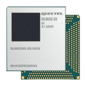
Figure 41: Top & Bottom Views of the Module NOTE Images above are for illustration purpose only and may differ from the actual module. For authentic appearance and label, please refer to the module received from Quectel. SG368Z_Series_Hardware_Design 101 / 113... -
Page 103: Storage, Manufacturing & Packaging
Smart Module Series Storage, Manufacturing & Packaging 8.1. Storage Conditions The module is provided with vacuum-sealed packaging. MSL of the module is rated as 3. The storage requirements are shown below. 1. Recommended storage condition: the temperature should be 23 ±5 ° C and the relative humidity should be 35–60 %. -
Page 104: Manufacturing And Soldering
Smart Module Series NOTE 1. To avoid blistering, layer separation and other soldering issues, extended exposure of the module to the air is forbidden. 2. Take out the module from the package and put it on high-temperature-resistant fixtures before baking. If shorter baking time is desired, see IPC/JEDEC J-STD-033 for the baking procedure. 3. - Page 105 Avoid using ultrasonic technology for module cleaning since it can damage crystals inside the module. Due to the complexity of the SMT process, please contact Quectel Technical Support in advance for any situation that you are not sure about, or any process (e.g. selective soldering, ultrasonic soldering) that is not mentioned in document [5].
-
Page 106: Packaging Specification
Smart Module Series 8.3. Packaging Specification This chapter describes only the key parameters and process of packaging. All figures below are for reference only. The appearance and structure of the packaging materials are subject to the actual delivery. The module adopts carrier tape packaging and details are as follow: 8.3.1. -
Page 107: Plastic Reel
Smart Module Series 8.3.2. Plastic Reel Figure 44: Plastic Reel Dimension Drawing Table 56: Plastic Reel Dimension Table (Unit: mm) øD1 øD2 72.5 8.3.3. Mounting Direction Figure 45: Mounting Direction SG368Z_Series_Hardware_Design 106 / 113... -
Page 108: Packaging Process
Smart Module Series 8.3.4. Packaging Process Place the module into the carrier tape and use the cover tape to cover it; then wind the heat-sealed carrier tape to the plastic reel and use the protective tape for protection. 1 plastic reel can load 200 modules. Place the packaged plastic reel, 1 humidity indicator card and 1 desiccant bag into a vacuum bag, vacuumize it. -
Page 109: Appendix References
Smart Module Series Appendix References Table 57: Related Documents Document Name [1] Quectel_SG368Z_Series_EVB_User_Guide [2] Quectel_SG368Z_Series_GPIO_Configuration [3] Quectel_SG368Z_Series_Reference_Design [4] Quectel_RF_Layout_Application_Note [5] Quectel_Module_SMT_Application_Note Table 58: Terms and Abbreviations Abbreviation Description Advanced Audio Coding Android Debug Bridge Alternating Current Application Processor Advanced RISC Machine Bluetooth Low Energy Bytes per second Basic Rate... - Page 110 Smart Module Series Clear To Send DFOTA Delta Firmware Upgrade Over-The-Air DPSK Differential Phase Shift Keying DQPSK Differential Quadrature Phase Shift Keying Display Serial Interface Digital Video Recorder Embedded DisplayPort Enhanced Data Rate Enhanced Full Rate Electromagnetic Interference eMMC Embedded Multimedia Card End Point eSCO Extended Synchronous Connection Oriented...
- Page 111 Smart Module Series High Speed High Throughput Inter-Integrated Circuit Inter-IC Sound IEEE Institute of Electrical and Electronics Engineers Internet Protocol Image Signal Processor Liquid Crystal Monitor Low Dropout Regulator Land Grid Array LPDDR Low-Power Double Data Rate LVDS Low-Voltage Differential Signaling Machine to Machine Media Access Control Modulation and Coding Scheme...
- Page 112 Smart Module Series PCIe Peripheral Component Interconnect Express Pulse Code Modulation Pulse Density Modulation Physical Layer Root Complex Radio Frequency Red Green Blue RGMII Reduced Gigabit Media Independent Interface RoHS Restriction of Hazardous Substances Request To Send SATA Serial Advanced Technology Attachment Synchronous Connection Oriented Secure Digital SDIO...
- Page 113 Smart Module Series VBAT Voltage at Battery (Pin) Very High Throughput Vmax Maximum Voltage Vmin Minimum Voltage Vnom Nominal Voltage VSWR Voltage Standing Wave Ratio WLAN Wireless Local Area Network Wi-Fi Protected Access Transmit & Receive Transmit UART Universal Asynchronous Receiver/Transmitter Ultra High Band Uplink UMTS...
- Page 114 WWAN Wireless Wide Area Network Modifications: Any changes or modifications not expressly approved by Quectel or the party responsible for compliance could void the user’s authority to operate the equipment and invalidate the regulatory approval. Host manufacturer must follow KDB Publication 996369 D04 Modulen Integration Guide.
- Page 115 5725~5850 MHz:3.3 dBi • The product is provided with an approved antenna. Use only supplied or approved antenna by Quectel. Any changes or modifications to the Antenna may void the regulatory approvals obtained for the product. • Host device must comply with FCC Part 15 antenna requirements •...
- Page 116 Smart Module Series and the FCC ID. The final host / module combination may also need to be evaluated against the FCC Part 15B criteria for unintentional radiators in order to be properly authorized for operation as a Part 15 digital device. The user’s manual or instruction manual for an intentional or unintentional radiator shall caution the user that changes or modifications not expressly approved by the party responsible for compliance could void the user's authority to operate the equipment.
- Page 117 Smart Module Series number”. Le produit hôte doit être correctement étiqueté pour identifier les modules dans le produit hôte. L'étiquette de certification d'Innovation, Sciences et Développement économique Canada d'un module doit être clairement visible en tout temps lorsqu'il est installédans le produit hôte; sinon, le produit hôte doit porter une étiquette indiquant le numéro de certification d'Innovation, Sciences et Développement économique Canada pour le module, précédé...
Need help?
Do you have a question about the SG368Z Series and is the answer not in the manual?
Questions and answers