
Related Manuals for Quectel SC200L Series


Summary of Contents for Quectel SC200L Series
- Page 1 SC200L Series (Dual-band Wi-Fi) Hardware Design Smart Module Series Version: 1.0 Date: 2021-09-17 Status: Released...
- Page 2 Smart Module Series At Quectel, our aim is to provide timely and comprehensive services to our customers. If you require any assistance, please contact our headquarters: Quectel Wireless Solutions Co., Ltd. Building 5, Shanghai Business Park Phase III (Area B), No.1016 Tianlin Road, Minhang District, Shanghai...
- Page 3 Except as otherwise set forth herein, nothing in this document shall be construed as conferring any rights to use any trademark, trade name or name, abbreviation, or counterfeit product thereof owned by Quectel or any third party in advertising, publicity, or other aspects.
-
Page 4: Safety Information
Manufacturers of the cellular terminal should notify users and operating personnel of the following safety information by incorporating these guidelines into all manuals of the product. Otherwise, Quectel assumes no liability for customers’ failure to comply with these precautions. -
Page 5: About The Document
Smart Module Series About the Document Revision History Version Date Author Description Shihao HUANG/ 2021-05-26 Creation of the document Shawn HU Shihao HUANG/ 2021-09-17 First official release Shawn HU SC200L_Series(Dual-band Wi-Fi)_Hardware_Design 4 / 111... -
Page 6: Table Of Contents
Smart Module Series Contents Safety Information ............................3 About the Document ........................... 4 Contents ............................... 5 Table Index ..............................8 Figure Index ............................... 10 Introduction ............................12 1.1. Special Mark ..........................12 Product Overview ..........................13 2.1. Frequency Bands and Functions ....................13 2.2. - Page 7 Smart Module Series 3.20.2. Reference Circuit Design for Earpiece Interface ............61 3.20.3. Reference Circuit Design for Headset Interface ............61 3.20.4. Reference Circuit Design for Loudspeaker Interface............. 62 3.20.5. Audio Signal Design Considerations ................62 3.21. Emergency Download Interface ....................63 Wi-Fi and Bluetooth ...........................
- Page 8 Smart Module Series 9.3.1. Carrier Tape ........................103 9.3.2. Plastic Reel ........................104 9.3.3. Packaging Process ...................... 104 10 Appendix References ........................106 SC200L_Series(Dual-band Wi-Fi)_Hardware_Design 7 / 111...
- Page 9 Smart Module Series Table Index Table 1: Special Mark ..........................12 Table 2: SC200L-CE* Frequency Bands....................13 Table 3: SC200L-EU Frequency Bands ..................... 14 Table 4: SC200L-AU* Frequency Bands....................14 Table 5: Key Features ..........................15 Table 6: I/O Parameters Definition ......................21 Table 7: Pin Description ..........................
- Page 10 Smart Module Series Table 42: Power Supply Ratings ........................ 81 Table 43: Operating and Storage Temperatures ..................82 Table 44: SC200L-CE* Power Consumption ..................... 82 Table 45: SC200L-EU Power Consumption ....................84 Table 46: SC200L-AU* Power Consumption ..................... 87 Table 47: SC200L-CE* RF Output Power ....................90 Table 48: SC200L-EU RF Output Power ....................
- Page 11 Smart Module Series Figure Index Figure 1: Functional Diagram ........................18 Figure 2: Pin Assignment (Perspective View) .................... 20 Figure 3: Voltage Drop Sample ........................33 Figure 4: Star Structure of Power Supply ....................34 Figure 5: Reference Circuit of Power Supply ..................... 34 Figure 6: Turn On the Module Using Driving Circuit ..................
- Page 12 Smart Module Series Figure 42: Module Bottom Dimensions (Bottom View) ................97 Figure 43: Recommended Footprint (Top View) ..................98 Figure 44: Top and Bottom Views ......................99 Figure 45: Recommended Reflow Soldering Thermal Profile ..............101 Figure 46: Carrier Tape Dimension Drawing .................... 103 Figure 47: Plastic Reel Dimension Drawing ....................
-
Page 13: Introduction
Smart Module Series Introduction This document, describing SC200L series (Dual-band Wi-Fi) module and its air and hardware interfaces connected to your applications, informs you of the interface specifications, electrical and mechanical details, as well as other related information of the module. -
Page 14: Product Overview
Smart Module Series Product Overview 2.1. Frequency Bands and Functions SC200L series (Dual-band Wi-Fi) is a series of smart LTE module based on Android operating system, and provides industrial grade performance. Its general features are listed below: ⚫ Supports LTE-FDD, LTE-TDD, HSDPA, HSUPA, WCDMA, EDGE, GSM and GPRS coverage. - Page 15 Smart Module Series GPS: 1575.42 ± 1.023 MHz GNSS GLONASS: 1597.5–1605.8 MHz BeiDou: 1561.098 ± 2.046 MHz Table 3: SC200L-EU Frequency Bands Mode Frequency bands LTE-FDD B1/B3/B5/B7/B8/B20/B28 LTE-TDD B38/B40/B41(200 MHz) WCDMA B1/B5/B8 900/1800 MHz 2402–2482 MHz Wi-Fi 802.11a/b/g/n/ac 5180–5825 MHz Bluetooth 5.0 2402–2480 MHz GPS: 1575.42 ±...
-
Page 16: Key Features
Smart Module Series The module is an SMD module with a total of 274 pins, including 146 LCC pins and 128 LGA pins. The size is only 40.5 mm × 40.5 mm × 2.85 mm, which can be embedded in various M2M product applications through pads. - Page 17 Smart Module Series GPRS Supports GPRS multi-slot level 33 (default 33) Coding format: CS-1, CS-2, CS-3 and CS-4 Max. 107 kbps (DL)/ Max. 85.6 kbps (UL) GSM Features EDGE Supports EDGE multi-slot level 33 (default 33) Supports GMSK and 8-PSK modulation and coding methods Downlink coding format: MCS 1–9 Uplink coding format: MCS 1–9 Max.
-
Page 18: Functional Diagram
Smart Module Series 2 UART interfaces: ⚫ UART0: 4-wire UART interface, supports RTS and CTS hardware flow UART Interfaces control, up to 3.25 Mbps ⚫ Debug UART: 2-wire UART interface, used for debugging by default Supports SD 3.0 SD Card Interface Supports 1.8 V or 3.0 V SD card Supports SD card hot-plug 2 (U)SIM interfaces... -
Page 19: Evb
Figure 1: Functional Diagram 2.4. EVB To help you design and test applications with the module, Quectel supplies an evaluation kit, which includes an evaluation board, a USB to RS-232 converter cable, a USB data cable, an earphone, antennas, etc. For more details, see document [1]. -
Page 20: Application Interfaces
Smart Module Series Application Interfaces 3.1. General Description The following chapters provide the detailed description of pins/interfaces listed below. ⚫ Power supply ⚫ USB interfaces ⚫ UART interfaces ⚫ (U)SIM interfaces ⚫ SD card interface ⚫ GPIO interfaces ⚫ I2C interfaces ⚫... -
Page 21: Pin Assignment
Smart Module Series 3.2. Pin Assignment The following figure shows the pin assignment of the module. GPIO_55 VBAT_BB GPIO_54 VBAT_BB BAT_ID CS_P CS_M RESERVED RESERVED RESERVED RESERVED RESERVED RESERVED RESERVED GPIO_07 GPIO_52 MIC1_P GPIO_155 MIC1_N MIC_ BIAS1 GPIO_154 MIC2_P GPIO_28 GPIO_23 EAR_P MIC2_N... -
Page 22: Pin Description
Smart Module Series 3.3. Pin Description Table 6: I/O Parameters Definition Type Description Analog Input Analog Output Analog Input/Output Digital Input Digital Output Digital Input/Output Open Drain Power Input Power Output Power Input/Output Table 7: Pin Description Power Supply Pin Name Description DC Characteristics Comment... - Page 23 Smart Module Series Power supply for LCD, TP and sensor. If it is used, connect an 2.80 V output Vnom = 2.80 V external capacitor to this LDO4_2V8 power supply max = 200 mA pin in parallel. See document [2] for details.
- Page 24 Smart Module Series Speaker output SPK_N Headphone right HPH_R channel output Headphone If it is not used, connect HPH_REF reference ground it to ground. Headphone left HPH_L channel output Headset HS_DET High level by default. insertion detect Headphone HPMIC_DET microphone detect Vmin = 2.20 V Microphone bias...
- Page 25 Smart Module Series USB differential USB 2.0 standard HUB_USB_DP data bus (+) compliant. 90 Ω differential impedance. USB differential Supports USB host HUB_USB_DM data bus (-) mode only and supports USB hub. (U)SIM Interfaces Pin Name Description DC Characteristics Comment This function is enabled (U)SIM2 card max=0.48 V...
- Page 26 Smart Module Series max = (U)SIM1 card 0.1 × USIM1_VDD USIM1_RST reset min = 0.9 × USIM1_VDD max = (U)SIM1 card 0.1 × USIM1_VDD USIM1_CLK clock min = 0.9 × USIM1_VDD max = 0.3 × USIM1_VDD min = (U)SIM1 card 0.7 ×...
- Page 27 Smart Module Series If a large-capacity T-Flash card is to be SD card power Vnom = 3.00 V connected, it is SD_VDD supply max = 400 mA recommended to add an LDO which can supply 1 A current. 1.8 V SD card: max = 0.19 V min = 1.58 V SD_CLK...
- Page 28 Smart Module Series max = 0.20 V LCD_RST LCD reset 1.85 V power domain. min = 1.46 V LCD tearing max = 0.48 V LCD_TE 1.85 V power domain. effect min = 1.39 V MIPI DSI clock DSI_CLK_N MIPI DSI clock DSI_CLK_P MIPI DSI data 0 DSI_LN0_N...
- Page 29 Smart Module Series MIPI clock of CSI0_CLK_N front camera (-) MIPI clock of CSI0_CLK_P front camera (+) MIPI lane 0 data CSI0_LN0_N of front camera MIPI lane 0 data CSI0_LN0_P of front camera Master clock of max = 0.20 V MCAM_MCLK rear camera min = 1.46 V...
- Page 30 Smart Module Series If it is not used, keep it max = 0.48 V VOL_DOWN Volume down open. min = 1.39 V 1.85 V power domain. RGB LED Interfaces Pin Name Description DC Characteristics Comment Connect it to the negative pole of LED. RGB_B LED (-) The maximum current is...
- Page 31 Smart Module Series Battery voltage The maximum input BAT_SNS detect voltage is 4.50 V. Fuel gauge CS_M If fuel gauge is not used, detect (-) connect these pins to Fuel gauge ground. CS_P detect (+) Externally pull this pin up to LDO1_1V85 with a 47 kΩ...
- Page 32 Smart Module Series General-purpose GPIO_49 input/output General-purpose GPIO_48 input/output General-purpose GPIO_156 input/output General-purpose GPIO_22 input/output General-purpose GPIO_23 input/output General-purpose GPIO_28 input/output General-purpose GPIO_154 input/output General-purpose GPIO_155 input/output General-purpose GPIO_52 input/output General-purpose Can be multiplexed into GPIO_07 input/output PWMC. General-purpose GPIO_54 input/output General-purpose GPIO_55...
-
Page 33: Power Supply
Smart Module Series GRFC Interfaces Pin Name Description DC Characteristics Comment Generic RF GRFC_7 control Generic RF GRFC_5 control Other Pins Pin Name Description DC Characteristics Comment You can force the module to enter Force the module max = 0.48 V emergency download USB_BOOT into emergency... -
Page 34: Voltage Stability Requirements
Smart Module Series 3.4.2. Voltage Stability Requirements The power supply range of the module is 3.50–4.20 V, and the recommended value is 3.80 V. The power supply performance, such as load capacity, voltage ripple, etc. directly influences the module’s performance and stability. Under ultimate conditions, the transient peak current of the module may surge up to 3 A. -
Page 35: Reference Design For Power Supply
Smart Module Series VBAT VBAT_RF VBAT_BB 100 μF 4.7 μF μF 100 nF 33 pF 10 pF 100 nF 33 pF 10 pF Module Figure 4: Star Structure of Power Supply 3.4.3. Reference Design for Power Supply The power design for the module is very important, as the performance of the module largely depends on the power source. -
Page 36: Turn On And Off The Module
Smart Module Series NOTE It is recommended to switch off the power supply when the module is in abnormal state, and then switch on the power to restart the module. The module supports battery charging function by default. If the above power supply design is adopted, please make sure the charging function is disabled by software, or connect VBAT to a Schottky diode in series to avoid the reverse current to the power supply IC. - Page 37 Smart Module Series The turning-on scenario is illustrated in the following figure. VBAT (Typ. 3.8 V) NOTE 2 PWRKEY > 2.5 s 607.4 ms LDO1_1V85 400 μs LDO4_2V8 Software Controlled > 1 s LDO2_1V8 LDO3_2V8 55 s Others ACTIVE Figure 8: Power-Up Timing NOTE When the module is powered on for the first time, its timing of power-up may be different from that shown above.
-
Page 38: Turn Off/Restart The Module
Smart Module Series 3.5.2. Turn Off/Restart the Module To turn off the module, you should drive the PWRKEY pin low for at least 1 s and then choose to turn off the module when the prompt window comes up. It can also be forced to restart by pulling down the PWRKEY key for at least 7 s. The restart timing is as follows: VBAT >... -
Page 39: Battery Charging And Management
Smart Module Series USIM2_VDD 1.80/2.95 3.7. Battery Charging and Management The module supports battery charging and the charger IC supports trickle charging, constant current charging and constant voltage charging modes. ⚫ Trickle charging: There are two steps in this mode. When the battery voltage is between 1.1 V and 2.05 V, a 70 mA trickle charging current is applied to the battery. -
Page 40: Usb Interfaces
Smart Module Series A reference design for battery charging circuit is shown as below. Adapter or USB USB_VBUS 47K 1% LDO1_1V85 VBAT BAT_SNS VBAT BAT_THERM 22 μF 1 μF 33 pF SC200L Battery 20 mΩ CS_P CS_M Figure 10: Reference Design for Battery Charging Circuit Mobile devices such as mobile phones and handheld POS systems are powered by batteries. - Page 41 Smart Module Series The following table shows the pin definition of USB1. Table 10: Pin Definition of USB1 Interface Pin Name Pin No. Description Comment Charging power input; Vmax = 9.20 V USB 5 V power input; USB_VBUS 141, 142 Vmin = 4.50 V USB/adaptor insertion Vnom = 5.00 V...
- Page 42 Smart Module Series The USB1 interface of the module supports OTG function. If you need this function, follow the design below to add an external 5 V power supply, which can provide 500 mA current. VBAT AW3605DNR 1.0 μH USB_VBUS VOUT VOUT 10 μF...
- Page 43 Smart Module Series The USB2 interface of the module only supports USB host mode. If you need this function, follow the design below to add an external 5 V power supply, which can provide 500 mA current. VBAT AW3605DNR 1.0 μH USB_VBUS2 VOUT VOUT...
-
Page 44: Uart Interfaces
Smart Module Series 3.9. UART Interfaces The module provides the following two UART interfaces: ⚫ UART0: 4-wire UART interface, supports RTS and CTS hardware flow control, up to 3.25 Mbps ⚫ Debug UART: 2-wire UART interface, used for debugging by default The following table shows the pin definition of UART interfaces. -
Page 45: U)Sim Interfaces
Smart Module Series The following figure is an example of connection between the module and PC. A voltage level translator and an RS-232 level translator chip are recommended to be added between the module and PC, as shown below: 1.85 V 3.3 V VCCA VCCB... - Page 46 Smart Module Series USIM1_RST (U)SIM1 card reset USIM1_CLK (U)SIM1 card clock USIM1_DATA (U)SIM1 card data (U)SIM1 card power Either 1.8 V or 2.95 V (U)SIM card USIM1_VDD supply is supported. The module supports (U)SIM card hot-plug function through USIM_DET (The function is enabled by default through software configuration).
-
Page 47: Sd Card Interface
Smart Module Series To ensure better performance and avoid damage to (U)SIM cards, please follow the criteria below in (U)SIM circuit design: ⚫ Place the (U)SIM card connector as close to the module as possible. Keep the trace length of (U)SIM card signals as less than 200 mm as possible. - Page 48 Smart Module Series A reference circuit for SD card interface is shown as below. SD_VDD SD_DATA2 P1-DAT2 SD_DATA3 P2-CD/DAT3 SD_CMD P3-CMD P4-VDD SD_CLK P5-CLK P6-VSS SD_DATA0 P7-DAT0 SD_DATA1 P8-DAT1 SD_DET DETECTIVE Module 4.7 μF 33 pF SD Card Connector Figure 19: Reference Circuit for SD Card Interface SD_VDD supplies power for the SD card and can provide up to 400 mA output current.
-
Page 49: Gpio Interfaces
Smart Module Series SD_DATA2 47.26 SD_DATA3 49.00 3.12. GPIO Interfaces The module has multiple GPIO interfaces with power domain of 1.85 V. The pin definition is listed below. Table 17: Pin Definition of GPIO Interfaces Pin Name Pin No. Default state Pin Description Comment GPIO_87... - Page 50 Smart Module Series GPIO_55 IN/PD General-purpose input/output Can be multiplexed GPIO_122 IN/PD General-purpose input/output into EXTINT12. GPIO_30 IN/PD General-purpose input/output GPIO_29 IN/PD General-purpose input/output Can be multiplexed GPIO_93 IN/PD General-purpose input/output into EXTINT8. Can be multiplexed GPIO_90 IN/PU General-purpose input/output into EXTINT5.
-
Page 51: I2C Interfaces
Smart Module Series 3.13. I2C Interfaces The module provides four I2C interfaces. All I2C interfaces are open-drain output with pull-up resistors inside the module, and the reference power domain is 1.85 V. Table 18: Pin Definition of I2C Interfaces Pin Name Pin No. -
Page 52: Adc Interface
Smart Module Series 3.15. ADC Interface The module provides one general-purpose analog-to-digital converter (ADC) interface, and the resolution of the ADC is up to 12 bits. Table 20: Pin Definition of ADC Interface Pin Name Pin No. Comment Pin Name General-purpose ADC The maximum input voltage is interface... - Page 53 Smart Module Series DSI_LN1_P MIPI DSI data 1 (+) DSI_LN2_N MIPI DSI data 2 (-) DSI_LN2_P MIPI DSI data 2 (+) DSI_LN3_N MIPI DSI data 3 (-) DSI_LN3_P MIPI DSI data 3 (+) The following are the reference designs for LCM interface. LDO4_2V 8 LDO_1P8 VBAT...
-
Page 54: Touch Panel Interface
Smart Module Series It is recommended to read the LCM ID register through MIPI when compatible design with other displays is required. If several LCM models share the same IC, it is recommended that the LCM module factory burn the OTP register to distinguish different screens. You can also connect the LCD_ID pin of LCM to GPIO pin of the module and distinguish different factory through level detection. -
Page 55: Camera Interfaces
Smart Module Series 1.85 V power domain. TP_RST TP reset Active low. TP_I2C_SCL TP I2C clock 1.85 V power domain, Can be used for other I2C devices. TP_I2C_SDA TP I2C data A reference design for touch panel interface is shown below. LDO4_2V8 LDO2_1V8 SDA 1.8 V... - Page 56 Smart Module Series Table 23: Pin Definition of Camera Interfaces Pin Name Pin No. Description Comment 1.80 V output power supply Vnom = 1.80 V LDO2_1V8 for camera DOVDD max = 200 mA 2.80 V output power supply Vnom = 2.80 V LDO3_2V8 for camera AVDD and AFVDD max = 150 mA...
- Page 57 Smart Module Series The following is a reference circuit design for dual-camera applications. LDO3 _2V8 LDO3 _ 2V8 1 μF AF_VDD 1.2 V VBAT AVDD DVDD GPIO _ 32 DOVDD LDO 2_1V8 MCAM_ RST MCAM_PWDN MCAM_MCLK CAM_I2C_ SDA CAM_I2C_ SCL CSI1_LN1_P CSI1_LN1_N CSI1_LN0_P...
-
Page 58: Mipi Design Considerations
Smart Module Series 3.18.1. MIPI Design considerations ⚫ Pay attention to the pin definitions of LCM and camera connectors to ensure they are connected correctly. ⚫ MIPI are high-speed signal lines, supporting maximum data rate up to 1.5 Gbps. The differential impedance should be controlled to 100 Ω. -
Page 59: Sensor Interfaces
Smart Module Series CSI1_LN0_N 14.13 -0.38 CSI1_LN0_P 13.75 CSI1_LN1_N 17.45 -0.37 CSI1_LN1_P 17.08 CSI0_CLK_N 18.52 0.41 CSI0_CLK_P 18.93 CSI0_LN0_N 19.76 0.05 CSI0_LN0_P 19.81 3.19. Sensor Interfaces The module supports communication with sensors via I2C interfaces, and it supports various sensors such as ALS/PS, accelerometer sensor, gyroscope sensor, geomagnetic sensor, etc. -
Page 60: Audio Interfaces
Smart Module Series 3.20. Audio Interfaces The module provides three analog input channels and three analog output channels. The following table shows the pin definition. Table 26: Pin Definition of Audio Interfaces Pin Name Pin No. Description Comment MIC1_P Microphone input for channel 1 (+) MIC1_N Microphone input for channel 1 (-) MIC2_P... -
Page 61: Reference Circuit Design For Microphone Interfaces
Smart Module Series ⚫ The module has three differential audio input channels. ⚫ The output voltage range of the two MIC_BIAS is programmable between 2.2 V and 3.0 V, and the maximum output current is 2 mA. ⚫ The earpiece interface uses differential output. ⚫... -
Page 62: Reference Circuit Design For Earpiece Interface
Smart Module Series 3.20.2. Reference Circuit Design for Earpiece Interface 33 pF EAR_P 100 pF EAR_N 33 pF Module Figure 26: Reference Circuit Design for Earpiece Interface 3.20.3. Reference Circuit Design for Headset Interface HPMIC_DET MIC_BIAS2 4.7 μF 1 μF MIC2_P 1.2K 1 μF... -
Page 63: Reference Circuit Design For Loudspeaker Interface
Smart Module Series 3.20.4. Reference Circuit Design for Loudspeaker Interface SPK_P EARP SPK_N C4 C5 Module Figure 28: Reference Circuit Design for Loudspeaker Interface 3.20.5. Audio Signal Design Considerations It is recommended to use the electret microphone with dual built-in capacitors (e.g. 10 pF and 33 pF) to filter out RF interference, thus reducing TDD noise. -
Page 64: Emergency Download Interface
Smart Module Series 3.21. Emergency Download Interface USB_BOOT is an emergency download interface. You can force the module to enter emergency download mode by pulling it down to ground during power-up. This is an emergency option when start-up failures or operational abnormalities occur. For firmware upgrade and debugging in the future, please reserve the following reference design. -
Page 65: Wi-Fi And Bluetooth
Smart Module Series Wi-Fi and Bluetooth The module provides a shared antenna interface ANT_WIFI/BT for Wi-Fi and Bluetooth functions. The impedance of the interface should be controlled to 50 Ω. You may connect external antennas such as PCB antenna, sucker antenna and ceramic antenna to the module via the interface to achieve Wi-Fi and Bluetooth functions. - Page 66 Smart Module Series 802.11g 54 Mbps 802.11n HT20 MCS0 802.11n HT20 MCS7 802.11n HT40 MCS0 802.11n HT40 MCS7 802.11a 6 Mbps 802.11a 54 Mbps 802.11n HT20 MCS0 802.11n HT20 MCS7 802.11n HT40 MCS0 802.11n HT40 MCS7 5 GHz 802.11ac VHT20 MCS0 802.11ac VHT20 MCS8...
-
Page 67: Bluetooth Overview
Smart Module Series 802.11n HT20 MCS7 802.11n HT40 MCS0 802.11n HT40 MCS7 802.11a 6 Mbps 802.11a 54 Mbps 802.11n HT20 MCS0 802.11n HT20 MCS7 802.11n HT40 MCS0 802.11n HT40 MCS7 5 GHz 802.11ac VHT20 MCS0 802.11ac VHT20 MCS8 802.11ac VHT40 MCS0 802.11ac VHT40 MCS9... -
Page 68: Bluetooth Performance
Smart Module Series Table 29: Bluetooth Data Rate and Versions Version Data rate Maximum Application Throughput 1 Mbit/s > 80 kbit/s 2.0+EDR 3 Mbit/s > 80 kbit/s 24 Mbit/s Reference 4.0 LE 48 Mbit/s Reference 5.0 LE Referenced specifications are listed below: ⚫... -
Page 69: Gnss
Smart Module Series GNSS The module integrates a GNSS engine (GEN 8C) which supports multiple positioning and navigation systems including GPS, GLONASS, and BeiDou. With an embedded LNA, the positioning accuracy of the module has been significantly improved. 5.1. GNSS Performance The following table lists the GNSS performance of the module in conduction mode. -
Page 70: Gnss Rf Design Guidelines
Smart Module Series 5.2. GNSS RF Design Guidelines Bad design of antenna and layout may cause reduced GNSS receiving sensitivity, longer GNSS positioning time, or reduced positioning accuracy. To avoid these, follow the design rules listed below: ⚫ Maximize the distance between the GNSS RF part and the GPRS RF part (including trace routing and antenna layout) to avoid mutual interference. -
Page 71: Antenna Interfaces
Smart Module Series Antenna Interfaces The module provides four antenna interfaces: main antenna, Rx-diversity antenna, Wi-Fi/Bluetooth antenna, and GNSS antenna respectively. The impedance of the antenna ports should be controlled to 50 Ω. 6.1. Main/Rx-diversity Antenna Interfaces The pin definition of main/Rx-diversity antenna interfaces is shown below. Table 32: Pin Definition of Main/Rx-diversity Antenna Interfaces Pin Name Pin No. - Page 72 Smart Module Series LTE-FDD B5 869–894 824–849 LTE-FDD B8 925–960 880–915 LTE-TDD B34 2010–2025 2010–2025 LTE-TDD B38 2570–2620 2570–2620 LTE-TDD B39 1880–1920 1880–1920 LTE-TDD B40 2300–2400 2300–2400 LTE-TDD B41 2535–2675 2535–2675 Table 34: SC200L-EU Module Operating Frequencies 3GPP Band Receive Transmit Unit EGSM900...
-
Page 73: Reference Circuit Design For Main And Rx-Diversity Antenna Interfaces
Smart Module Series Table 35: SC200L-AU* Module Operating Frequencies 3GPP Band Receive Transmit Unit GSM850 869–894 824–849 EGSM900 925–960 880–915 DCS1800 1805–1880 1710–1785 PCS1900 1930–1990 1850–1910 WCDMA B1 2110–2170 1920–1980 WCDMA B2 1930–1990 1850–1910 WCDMA B4 2110–2155 1710–1755 WCDMA B5 869–894 824–849 WCDMA B8... -
Page 74: Wi-Fi/Bluetooth Antenna Interface
Smart Module Series Main antenna ANT_MAIN Diversity antenna ANT_DRX Module Figure 30: Reference Circuit Design for Main and Rx-diversity Antenna Interfaces 6.2. Wi-Fi/Bluetooth Antenna Interface Table 36: Pin Definition of Wi-Fi/Bluetooth Antenna Interface Pin Name Pin No. Description Comment Wi-Fi/Bluetooth antenna 50 Ω... -
Page 75: Gnss Antenna Interface
Smart Module Series A reference circuit design for Wi-Fi/Bluetooth antenna interface is shown as below. A π-type matching circuit is recommended to be reserved for better RF performance. The capacitors are not mounted by default and the resistor is 0 Ω. ANT_WIFI/BT Module Figure 31: Reference Circuit Design for Wi-Fi/Bluetooth Antenna Interface... -
Page 76: Reference Circuit Design For Passive Antenna
Smart Module Series 6.3.1. Reference Circuit Design for Passive Antenna GNSS antenna interface supports passive ceramic antennas and other types of passive antennas. A reference circuit design is given below. Passive Antenna ANT_GNSS Module Figure 32: Reference Circuit Design for GNSS Passive Antenna NOTE When the passive antenna is placed far away from the module (that is, the antenna trace is long) and the external loss is more than 2 dB, it is recommended to add an external LNA circuit for better GNSS... -
Page 77: Reference Design Of Rf Layout
Smart Module Series 6.5. Reference Design of RF Layout For user’s PCB, the characteristic impedance of all RF traces should be controlled as 50 Ω. The impedance of the RF traces is usually determined by the trace width (W), the materials’ dielectric constant, the distance between signal layer and reference ground (H), and the clearance between RF trace and ground (S). - Page 78 Smart Module Series Figure 36: Coplanar Waveguide Line Design on a 4-layer PCB (Layer 3 as Reference Ground) Figure 37: Coplanar Waveguide Line Design on a 4-layer PCB (Layer 4 as Reference Ground) To ensure RF performance and reliability, follow the principles below in RF layout design: ⚫...
-
Page 79: Antenna Installation
Smart Module Series 6.6. Antenna Installation 6.6.1. Antenna Requirements The following table shows the requirements on main antenna, Rx-diversity, Wi-Fi/Bluetooth antenna and GNSS antenna. Table 40: Antenna Requirements Type Requirements VSWR: ≤ 2 Gain: 1 dBi Max Input Power: 50 W Input Impedance: 50 Ω... -
Page 80: Recommended Rf Connector For Antenna Installation
Smart Module Series 6.6.2. Recommended RF Connector for Antenna Installation If RF connector is used for antenna connection, it is recommended to use the U.FL-R-SMT connector provided by Hirose. Figure 38: Dimensions of the U.FL-R-SMT Connector (Unit: mm) U.FL-LP serial connectors listed in the following figure can be used to match the U.FL-R-SMT. Figure 39: Mechanicals of U.FL-LP Connectors SC200L_Series(Dual-band Wi-Fi)_Hardware_Design 79 / 111... - Page 81 Smart Module Series The following figure describes the space factor of mated connector. Figure 40: Space Factor of Mated Connector (Unit: mm) For more details, please visit http://www.hirose.com. SC200L_Series(Dual-band Wi-Fi)_Hardware_Design 80 / 111...
-
Page 82: Reliability, Radio And Electrical Characteristics
Smart Module Series Reliability, Radio and Electrical Characteristics 7.1. Absolute Maximum Ratings Absolute maximum ratings for power supply and voltage on digital and analog pins of the module are listed in the following table. Table 41: Absolute Maximum Ratings Parameter Min. -
Page 83: Operating And Storage Temperatures
Smart Module Series Peak supply Maximum power control level at current (during 1.80 VBAT EGSM900 transmission slot) USB_VBUS 4.50 9.20 7.3. Operating and Storage Temperatures The operating and storage temperatures are listed in the following table. Table 43: Operating and Storage Temperatures Parameter Min. - Page 84 Smart Module Series Sleep (USB disconnected) @ DRX = 9 Sleep (USB disconnected) @ DRX = 5 Sleep (USB disconnected) @ DRX = 6 LTE-FDD supply current Sleep (USB disconnected) @ DRX = 7 Sleep (USB disconnected) @ DRX = 8 Sleep (USB disconnected) @ DRX = 5 Sleep (USB disconnected) @ DRX = 6 LTE-TDD supply current...
- Page 85 Smart Module Series EGSM900 (1UL/4DL) @ PCL 8 EGSM900 (2UL/3DL) @ PCL 8 EGSM900 (3UL/2DL) @ PCL 8 EGSM900 (4UL/1DL) @ PCL 8 EDGE data transfer DCS1800 (1UL/4DL) @ PCL 2 DCS1800 (2UL/3DL) @ PCL 2 DCS1800 (3UL/2DL) @ PCL 2 DCS1800 (4UL/1DL) @ PCL 2 B1 (HSDPA) @ max power B8 (HSDPA) @ max power...
- Page 86 Smart Module Series Sleep (USB disconnected) @ DRX = 2 GSM/GPRS supply current Sleep (USB disconnected) @ DRX = 5 Sleep (USB disconnected) @ DRX = 9 Sleep (USB disconnected) @ DRX = 6 Sleep (USB disconnected) @ DRX = 7 WCDMA supply current Sleep (USB disconnected) @ DRX = 8 Sleep (USB disconnected) @ DRX = 9...
- Page 87 Smart Module Series EGSM900 (2UL/3DL) @ PCL 5 EGSM900 (3UL/2DL) @ PCL 5 EGSM900 (4UL/1DL) @ PCL 5 DCS1800 (1UL/4DL) @ PCL 0 DCS1800 (2UL/3DL) @ PCL 0 DCS1800 (3UL/2DL) @ PCL0 DCS1800 (4UL/1DL) @ PCL 0 EGSM900 (1UL/4DL) @ PCL 8 EGSM900 (2UL/3DL) @ PCL 8 EGSM900 (3UL/2DL) @ PCL 8 EGSM900 (4UL/1DL) @ PCL 8...
- Page 88 Smart Module Series LTE-FDD B8 @ max power LTE-FDD B20 @ max power LTE-FDD B28(A + B) @ max power LTE-TDD B38 @ max power LTE-TDD B40 @ max power LTE-TDD B41 @ max power Table 46: SC200L-AU* Power Consumption Description Conditions Typ.
- Page 89 Smart Module Series GSM850 @ PCL 5 GSM850 @ PCL 12 GSM850 @ PCL 19 EGSM900 @ PCL 5 EGSM900 @ PCL 12 EGSM900 @ PCL 19 GSM voice call DCS1800 @ PCL 0 DCS1800 @ PCL 7 DCS1800 @ PCL 15 PCS1900 @ PCL 0 PCS1900 @ PCL 7 PCS1900 @ PCL 15...
- Page 90 Smart Module Series DCS1800 (1UL/4DL) @ PCL 0 DCS1800 (2UL/3DL) @ PCL 0 DCS1800 (3UL/2DL) @ PCL0 DCS1800 (4UL/1DL) @ PCL 0 PCS1900 (1UL/4DL) @ PCL 0 PCS1900 (2UL/3DL) @ PCL 0 PCS1900 (3UL/2DL) @ PCL 0 PCS1900 (4UL/1DL) @ PCL 0 GSM850 (1UL/4DL) @ PCL 8 GSM850 (2UL/3DL) @ PCL 8 GSM850 (3UL/2DL) @ PCL 8...
-
Page 91: Tx Power
Smart Module Series B2 (HSDPA) @ max power B4 (HSDPA) @ max power B5 (HSDPA) @ max power B8 (HSDPA) @ max power B1 (HSUPA) @ max power B2 (HSUPA) @ max power B4 (HSUPA) @ max power B5 (HSUPA) @ max power B8 (HSUPA) @ max power LTE-FDD B1 @ max power LTE-FDD B2 @ max power... - Page 92 Smart Module Series DCS1800 WCDMA B1 WCDMA B8 LTE-FDD B1 LTE-FDD B3 LTE-FDD B5 LTE-FDD B8 LTE-FDD B34 LTE-TDD B38 LTE-TDD B39 LTE-TDD B40 LTE-TDD B41 Table 48: SC200L-EU RF Output Power Frequency Max. Min. EGSM900 DCS1800 WCDMA B1 WCDMA B5 WCDMA B8 LTE-FDD B1 LTE-FDD B3...
- Page 93 Smart Module Series LTE-FDD B20 LTE-FDD B28(A + B) LTE-TDD B38 LTE-TDD B40 LTE-TDD B41 Table 49: SC200L-AU* RF Output Power Frequency Max. Min. GSM850 EGSM900 DCS1800 PCS1900 WCDMA B1 WCDMA B2 WCDMA B4 WCDMA B5 WCDMA B8 LTE-FDD B1 LTE-FDD B2 LTE-FDD B3 LTE-FDD B4...
-
Page 94: Rx Sensitivity
Smart Module Series LTE-TDD B38 NOTE In GPRS 4-slot TX mode, the maximum output power is reduced by 3 dB. This design conforms to the GSM specification as described in Chapter 13.16 of 3GPP TS 51.010-1. 7.6. Rx Sensitivity The following table shows the conducted RF receiving sensitivity of the module. Table 50: SC200L-CE* RF Receiving Sensitivity... - Page 95 Smart Module Series Table 51: SC200L-EU RF Receiving Sensitivity Frequency Band Primary Diversity SIMO 3GPP (SIMO) EGSM900 -102.4 dBm DCS1800 -102.4 dBm WCDMA B1 -106.7 dBm WCDMA B5 -104.7 dBm WCDMA B8 -103.7 dBm LTE-FDD B1 (10 MHz) -96.3 dBm LTE-FDD B3 (10 MHz) -93.3 dBm LTE-FDD B5 (10 MHz)
-
Page 96: Esd
Smart Module Series WCDMA B2 -104.7 dBm WCDMA B4 -106.7 dBm WCDMA B5 -104.7 dBm WCDMA B8 -103.7 dBm LTE-FDD B1 (10 MHz) -96.3 dBm LTE-FDD B2 (10 MHz) -94.3 dBm LTE-FDD B3 (10 MHz) -93.3 dBm LTE-FDD B4 (10 MHz) -96.3 dBm LTE-FDD B5 (10 MHz) -94.3 dBm... -
Page 97: Mechanical Information
Smart Module Series Mechanical Information This chapter describes the mechanical dimensions of the module. All dimensions are measured in millimeter (mm), and the dimension tolerances are ± 0.2 mm unless otherwise specified. 8.1. Mechanical Dimensions Pin 1 Top view Side view Figure 41: Module Top and Side Dimensions SC200L_Series(Dual-band Wi-Fi)_Hardware_Design 96 / 111... - Page 98 Smart Module Series Pin 1 Figure 42: Module Bottom Dimensions (Bottom View) NOTE The package warpage level of the module conforms to JEITA ED-7306 standard. SC200L_Series(Dual-band Wi-Fi)_Hardware_Design 97 / 111...
-
Page 99: Recommended Footprint
Smart Module Series 8.2. Recommended Footprint Figure 43: Recommended Footprint (Top View) NOTE Keep at least 3 mm between the module and other components on the motherboard to improve soldering quality and maintenance convenience. All RESERVED pins should be kept open and MUST NOT be connected to ground. SC200L_Series(Dual-band Wi-Fi)_Hardware_Design 98 / 111... -
Page 100: Top And Bottom Views
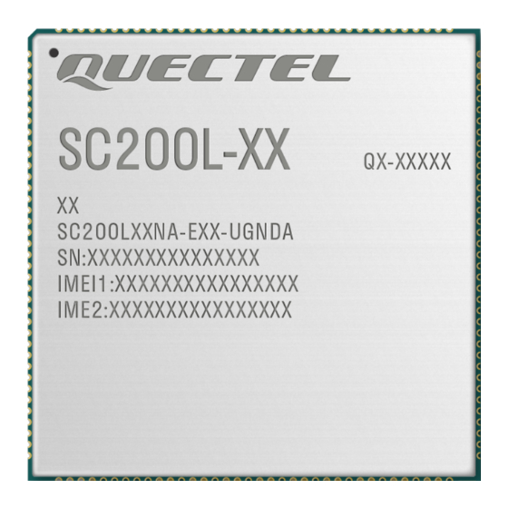
8.3. Top and Bottom Views Figure 44: Top and Bottom Views NOTE Images above are for illustration purpose only and may differ from the actual module. For authentic appearance and label, please refer to the module received from Quectel. SC200L_Series(Dual-band Wi-Fi)_Hardware_Design 99 / 111... -
Page 101: Storage, Manufacturing And Packaging
Smart Module Series Storage, Manufacturing and Packaging 9.1. Storage Conditions The module is provided with vacuum-sealed packaging. MSL of the module is rated as 3. The storage requirements are shown below. 1. Recommended Storage Condition: The temperature should be 23 ± 5 ° C and the relative humidity should be 35–60 %. -
Page 102: Manufacturing And Soldering
Smart Module Series NOTE 1. To avoid blistering, layer separation and other soldering issues, extended exposure of the module to the air is forbidden. 2. Take out the module from the package and put it on high-temperature-resistant fixtures before baking. All modules must be soldered to PCB within 24 hours after the baking, otherwise put them in the drying oven. - Page 103 2. Avoid using ultrasonic technology for module cleaning since it can damage crystals inside the module. 3. Due to the complexity of the SMT process, please contact Quectel Technical Supports in advance for any situation that you are not sure about, or any process (e.g. selective soldering, ultrasonic soldering) that is not mentioned in document [5].
-
Page 104: Packaging Specifications
Smart Module Series 9.3. Packaging Specifications The module adopts carrier tape packaging and details are as follows: 9.3.1. Carrier Tape Dimension details are as follows: Figure 46: Carrier Tape Dimension Drawing Table 55: Carrier Tape Dimension Table (Unit: mm) 41.2 41.2 34.2 1.75... - Page 105 Smart Module Series 9.3.2. Plastic Reel Figure 47: Plastic Reel Dimension Drawing Table 56: Plastic Reel Dimension Table (Unit: mm) øD1 øD2 72.5 9.3.3. Packaging Process Place the module into the carrier tape and use the cover tape to cover them; then wind the heat-sealed carrier tape to the plastic reel and use the protective tape for protection.
- Page 106 Smart Module Series Place the vacuum-packed plastic reel into a pizza box. Put 4 pizza boxes into 1 carton and seal it. One carton can pack 800 modules. Figure 48: Packaging Process SC200L_Series(Dual-band Wi-Fi)_Hardware_Design 105 / 111...
- Page 107 Smart Module Series Appendix References Table 57: Related Documents Document Name [1] Quectel_Smart_EVB_G2_User_Guide [2] Quectel_SC200L_Series(Dual-band_Wi-Fi)_Reference_Design [3] Quectel_SC200L_Series(Dual-band_Wi-Fi)_Pin_Description_and_GPIO_Configuration [4] Quectel_RF_Layout_Application_Note [5] Quectel_Module_Secondary_SMT_Application_Note Table 58: Terms and Abbreviations Abbreviation Description Analog-to-Digital Converter Ambient Light Sensor Adaptive Multi-rate Access Point Advanced RISC Machine Baseband Bluetooth Low Energy Bits per Second...
- Page 108 Smart Module Series Camera Serial Interface Clear to Send Digital Cellular System Downlink DPSK Differential Phase Shift Keying DQPSK Differential Quadrature Reference Phase Shift Keying Discontinuous Reception Display Serial Interface Electret Condenser Microphone EDGE Enhanced Data Rate for GSM Evolution Enhanced Data Rate Enhanced Full Rate EGSM...
- Page 109 Smart Module Series GNSS Global Navigation Satellite System GPIO General Purpose Input/Output GPRS General Packet Radio Service Global Positioning System Graphics Processing Unit GRFC Generic RF control Global System for Mobile Communications High Definition Plus Half Rate High Speed HSDPA High Speed Downlink Packet Access HSUPA High Speed Uplink Packet Access...
- Page 110 Smart Module Series Light Emitting Diode Land Grid Array Low Noise Amplifier LPDDR Low-Power Double Data Rate Long-Term Evolution Machine to Machine Media Access Control Modulation and Coding Scheme MEMS Micro-Electro-Mechanical System MIPI Mobile Industry Processor Interface Megapixel Moisture Sensitivity Levels Negative Temperature Coefficient Over-the-Air Upgrade On-The-Go...
- Page 111 Smart Module Series Proximity Sensor Pulse Width Modulation Phase Shift Keying Quadrature Amplitude Modulation QPSK Quadrature Phase Shift Keying Radio Frequency RoHS Restriction of Hazardous Substances Request to Send Surface Acoustic Wave Synchronous Connection Oriented Secure Digital SIMO Single Input Multiple Output Surface Mount Device Short Message Service Surface Mount Technology...
- Page 112 Smart Module Series (U)SIM (Universal) Subscriber Identity Module VBAT Voltage at Battery (Pin) Vmax Maximum Voltage Vnom Nominal Voltage Vmin Minimum Voltage Minimum High-level Input Voltage Maximum Low-level Input Voltage Minimum High-level Output Voltage Maximum Low-level Output Voltage WAPI WLAN Authentication and Privacy Infrastructure WCDMA Wideband Code Division Multiple Access WLAN...
Need help?
Do you have a question about the SC200L Series and is the answer not in the manual?
Questions and answers