Table of Contents
Advertisement
Advertisement
Table of Contents

Related Manuals for Xilinx VCK190 Series


Summary of Contents for Xilinx VCK190 Series
- Page 1 VCK190 Evaluation Board User Guide UG1366 (v1.0) January 7, 2021...
- Page 2 Revision History Revision History The following table shows the revision history for this document. Section Revision Summary 01/07/2021 Version 1.0 Initial release. UG1366 (v1.0) January 7, 2021 www.xilinx.com Send Feedback VCK190 Board User Guide...
- Page 3 ........... 23 Overview.............................23 Component Descriptions......................23 Appendix A: VITA 57.4 FMCP Connector Pinouts ......... 69 Overview.............................69 Appendix B: Xilinx Design Constraints ............. 70 Overview.............................70 Appendix C: Pmod FMC ....................71 Pin Mapping Pmod to FMC...................... 72 Appendix D: Regulatory and Compliance Information ......74...
- Page 4 Appendix E: Additional Resources and Legal Notices ......76 Xilinx Resources.........................76 Documentation Navigator and Design Hubs.................76 References..........................77 Please Read: Important Legal Notices................... 78 UG1366 (v1.0) January 7, 2021 www.xilinx.com Send Feedback VCK190 Board User Guide...
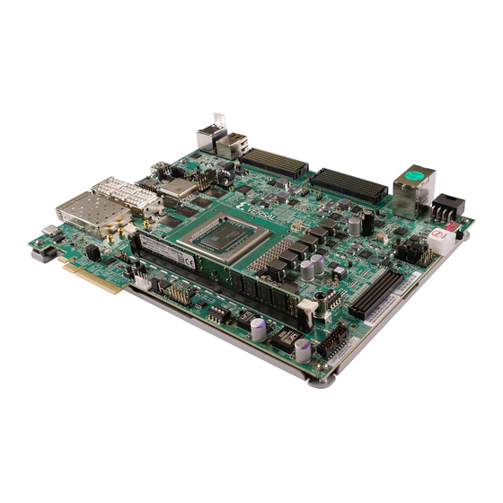
- Page 5 Chapter 1: Introduction Chapter 1 Introduction Overview The VCK190 evaluation board features the Xilinx ® Versal™ ACAP XCVC1902 device. The VCK190 board enables the demonstration, evaluation, and development of the applications listed here, as well as other customer applications. • Storage acceleration •...
- Page 6 The following table lists the models for the VCK190 evaluation board. See the VCK190 Evaluation Board product page for details. Table 1: Models of VCK190 Evaluation Boards Description Xilinx Versal ACAP VCK190 evaluation kit, encryption disabled, no secure boot EK-VCK190-G-ED support EK-VCK190-G-ED-J...
- Page 7 Design Process Documentation Board System Design. Additional Resources Appendix E: Additional Resources and Legal Notices for references to documents, files, and resources relevant to the VCK190 evaluation board. UG1366 (v1.0) January 7, 2021 www.xilinx.com Send Feedback VCK190 Board User Guide...
- Page 8 LP_MI0[0:25] Bank 502 GTY3 Bank 200 XPIO XPIO XPIO XPIO Triplet 1 Triplet 2 Triplet 3 Triplet 4 DDR4 72-bit LPDDR4 LPDDR4 UDIMM 2x (1x32) 2x (1x32) FMC+_01 FMC+_02 X23196-121620 UG1366 (v1.0) January 7, 2021 www.xilinx.com Send Feedback VCK190 Board User Guide...
- Page 9 XPIO triplet 1 (banks 700, 701, 702) ○ • Two LPDDR4 interfaces (2x32-bit 4 GB components each) XPIO triplets 2 (banks 703, 704, 705) and 4 (banks 709, 710, 711) ○ UG1366 (v1.0) January 7, 2021 www.xilinx.com Send Feedback VCK190 Board User Guide...
- Page 10 ○ Gen2 8-lane (x8) ○ Gen3 8-lane (x8) ○ Gen4 8-lane (x8) ○ • PS PMC MIO connectivity PS MIO[0:12]: boot configuration header ○ - DC QSPI support UG1366 (v1.0) January 7, 2021 www.xilinx.com Send Feedback VCK190 Board User Guide...
- Page 11 The VCK190 provides a rapid prototyping platform using the XCVC1902-2VSVA2197 device. See the Versal Architecture and Product Data Sheet: Overview (DS950) for a feature set overview, description, and ordering information. UG1366 (v1.0) January 7, 2021 www.xilinx.com Send Feedback VCK190 Board User Guide...
- Page 12 VCK190 evaluation board website for the XDC listing and board schematics. Environmental Temperature Operating: 0°C to +45°C Storage: -25°C to +60°C Humidity 10% to 90% non-condensing Operating Voltage +12 V UG1366 (v1.0) January 7, 2021 www.xilinx.com Send Feedback VCK190 Board User Guide...
- Page 13 Board Component Location The following figure shows the VCK190 board component locations. Each numbered component shown in the figure is keyed to the table in Board Component Descriptions. UG1366 (v1.0) January 7, 2021 www.xilinx.com Send Feedback VCK190 Board User Guide...
- Page 14 Figure 3: Evaluation Board Component Locations Round callout references a component Square callout references a component on the front side of the board on the back side of the board X24958-121420 UG1366 (v1.0) January 7, 2021 www.xilinx.com Send Feedback VCK190 Board User Guide...
- Page 15 HDMI XMT, TMDS to HDMI level TI SN65DP159RGZ, TE 1888811-1 U43,P2A(UPR) shifter retimer, 0x22, 0xBC dual port HDMI RCV TMDS retimer, 0x0B, TI TMDS181IRGZT, TE 1888811-1 U55,P2B(LWR) dual port 0xB8 UG1366 (v1.0) January 7, 2021 www.xilinx.com Send Feedback VCK190 Board User Guide...
- Page 16 ACAP U1 REF CLK, 33.33 MHz, Silicon Labs SI570JAC000900DG 1.8V CMOS, 0x5D PCIe 1:2 buffer, 100 MHz, 3.3V IDT 85411AMLF LVDS HDMI jitter atten., 148.50 MHz, IDT 8T49N241-994NLGI 3.3V LVDS, 0x6C UG1366 (v1.0) January 7, 2021 www.xilinx.com Send Feedback VCK190 Board User Guide...
- Page 17 The following figure shows the VCK190 board jumper header and switch locations. Each numbered component shown in the figure is keyed to the applicable table in this section. Both tables reference the respective schematic page numbers. UG1366 (v1.0) January 7, 2021 www.xilinx.com Send Feedback VCK190 Board User Guide...
- Page 18 The following table lists the default jumper settings. Table 3: Default Jumper Settings Callout Schematic Ref. Des. Function Default Number Page SYSMON VREFP 1-2: 1.024V VREFP connected to ACAP 2-3: VREFP connected to GND UG1366 (v1.0) January 7, 2021 www.xilinx.com Send Feedback VCK190 Board User Guide...
- Page 19 ULPI USB3320 U99 USB conn. J308 shield select J300 1-2: J308 shield directly to GND 2-3: J308 shield capacitor C2762 to GND IP4856 U104 VERSAL_SD1_REF voltage select J301 1-2: UTIL_3V3 2-3: GND UG1366 (v1.0) January 7, 2021 www.xilinx.com Send Feedback VCK190 Board User Guide...
- Page 20 Mode = SW1[4:1] = Mode[3:0] JTAG = ON,ON,ON,ON = 0000 QSPI32 = ON,ON,OFF,ON = 0010 SD = OFF,OFF,OFF,ON = 1110 Reserved for Xilinx = OFF,OFF,OFF,OFF = 1111 ® JTAG MUX select 2-pole DIP switch Switch OFF = 1 = High; ON = 0 = Low...
- Page 21 Settings" table in Versal ACAP Configuration On the 3-pin JTAG MUX, enable header J37 (2-pin jumper block installed on pins 1-2) to ○ inhibit the JTAG MUX (hi-Z mode) UG1366 (v1.0) January 7, 2021 www.xilinx.com Send Feedback VCK190 Board User Guide...
- Page 22 Versal ACAP Configuration. 3. Power-cycle the VCK190 or press the POR pushbutton SW2. SW2 is callout 35 in the "Evaluation Board Component Locations" figure in Board Component Location. UG1366 (v1.0) January 7, 2021 www.xilinx.com Send Feedback VCK190 Board User Guide...
- Page 23 Encryption Key Battery Backup Circuit The XCVC1902 ACAP U1 implements bitstream encryption key technology. The VCK190 board provides the encryption key backup battery circuit shown in the following figure. UG1366 (v1.0) January 7, 2021 www.xilinx.com Send Feedback VCK190 Board User Guide...
- Page 24 HDIO_UART4_TX/RX XPIO Bank 700 VCC1V2_DDR4 1.2V DDR4_DIMM1_DQ[32:63], CB[0:7], ADDR/CTRL; DDR4_DIMM1_CLK; Si570 U2 200 MHz XPIO Bank 701 VCC1V2_DDR4 1.2V DDR4_DIMM1_DQ[24:31], ADDR/CTRL XPIO Bank 702 VCC1V2_DDR4 1.2V DDR4_DIMM1_DQ[0:23], CB[0:7] UG1366 (v1.0) January 7, 2021 www.xilinx.com Send Feedback VCK190 Board User Guide...
- Page 25 DDR4 DIMM socket J45. Figure 6: DDR4 DIMM Memory XPIO Triplet 1 DDR4 72-bit UDIMM X23197-120120 The VCK190 board is shipped with a DDR4 UDIMM installed: • Manufacturer: Micron UG1366 (v1.0) January 7, 2021 www.xilinx.com Send Feedback VCK190 Board User Guide...
- Page 26 MTA9ADF1G72AZ-3GE1 data sheet at the Micron website. The ACAP connections for the feature described in this section are documented in the VCK190 board XDC file, referenced in Appendix B: Xilinx Design Constraints. LPDDR4 Component Memory [Figure 3, callout 3 and 4] The VCK190 board hosts two LPDDR4 memory systems, each with a component configuration of 2x (1x32-bit component).
- Page 27 Micron MT53D512M32D2DS data sheet at the Micron website. The detailed ACAP connections for the feature described in this section are documented in the VCK190 board XDC file, referenced in Appendix B: Xilinx Design Constraints. System Reset POR_B [Figure...
- Page 28 GEM1 U103.6 USB3320 U99 reset gate PCIE_PWRBRK_B GEM1 USB3320 U99 CAN1_TXD GEM1 USB3320 U99 CAN1_RXD GEM1 USB3320 U99 UART0 GEM1 USB3320 U99 UART0 GEM1 USB3320 U99 I2C1 GEM1 UG1366 (v1.0) January 7, 2021 www.xilinx.com Send Feedback VCK190 Board User Guide...
- Page 29 X-EBM-01 QSPI external daughter card installed on J212. The detailed ACAP connections for the feature described in this section are documented in the VCK190 board XDC file, referenced in Appendix B: Xilinx Design Constraints. The XCVC1902 MIO connector J212 pinout is listed in the following figure.
- Page 30 USB controller IP and the PHY device, which drives the physical USB bus. Using the ULPI standard reduces the interface pin count between the USB controller IP and the PHY device. UG1366 (v1.0) January 7, 2021 www.xilinx.com Send Feedback VCK190 Board User Guide...
- Page 31 Figure 10: USB3320 USB2.0 Connector J308 Shield Connection Options X24950-121420 The detailed ACAP connections for the feature described in this section are documented in the VCK190 board XDC file, referenced in Appendix B: Xilinx Design Constraints. PMC MIO[26:36, 51] Bank 501: Secure Digital (SD) Card IF (J302)
- Page 32 Aries Adapter Pin Number IP4856CX25 Pin Number IP4856CX25 Pin Name CLK_IN CMD_H CLK_FB VLDO VSD_REF DIR_0 VSUPPLY VCCA DIR_CMD DATA0_H DATA3_H DATA1_H DIR_1_3 DATA2_H DATA1_SD DATA0_SD CLK_SD CMD_SD DATA3_SD DATA2_SD ENABLE UG1366 (v1.0) January 7, 2021 www.xilinx.com Send Feedback VCK190 Board User Guide...
- Page 33 The detailed ACAP connections for the feature described in this section are documented in the VCK190 board XDC file, referenced in Appendix B: Xilinx Design Constraints. PS MIO[37] ZU4 System Controller GPIO The ACAP PS bank 501 MIO37 is connected to the ZU4 system controller U125 bank 500 MIO11 pin AE17.
- Page 34 See the NXP TJA1057GT/3J data sheet at the Nexperia website for CAN-bus transceiver details. The detailed ACAP connections for the feature described in this section are documented in the VCK190 board XDC file, referenced in Appendix B: Xilinx Design Constraints. PMC MIO[42:43] UART0 [Figure 3, callout 8] This is the primary Versal ACAP PS-side UART interface.
- Page 35 Future Technology Devices International Ltd website. The detailed ACAP connections for the feature described in this section are documented in the VCK190 board XDC file, referenced in Appendix B: Xilinx Design Constraints. PMC MIO[46:47] I2C0, PMC MIO[44:45] I2C1 I2C Bus Overview The following figure shows an overview of the I2C0 and I2C1 bus connections.
- Page 36 INA226 power monitors, as well as three SI570 components via the U33 TCA9548A switch. TCA6416A U233 is pin-strapped to respond to I2C address 0x20. The TCA9548A U33 switch is set to 0x74. UG1366 (v1.0) January 7, 2021 www.xilinx.com Send Feedback VCK190 Board User Guide...
- Page 37 See the "I2C0 Bus Topology" figure. TCA6416AU233 Addr. 0x20 I2C0_SCL MAX6643_OT_B (1) OT_B MAX6643 MAX6643_FANFAIL_B (1) FANFAIL_B MAX6643 PMBUS2_INA226_ALERT (1) ALERT 14x INA226 INA226 MAX6643_FULLSPD (1) FULLSPD MAX6643 FMCP1_FMC_PRSNT_M2C_B PRSNT_M2C_L J51(H) ASP_184329_01 FMCP2_FMC_PRSNT_M2C_B PRSNT_M2C_L J53(H) ASP_184329_01 UG1366 (v1.0) January 7, 2021 www.xilinx.com Send Feedback VCK190 Board User Guide...
- Page 38 P02-P03 NC U166, U168, U172, U173, U174, U176, U177, U178, PMBUS2_INA226_ALERT U180, U182, U184 ,U186, U188, U234 INA226, U125 ZU4EG P05-P06 NC MAX6643_FULLSPD U64 MAX6643 FMCP1_FMC_PRSNT_M2C_B J51 FMCP HSPC UG1366 (v1.0) January 7, 2021 www.xilinx.com Send Feedback VCK190 Board User Guide...
- Page 39 For more information on the TCA9548A and TCA6416A, see the Texas Instruments website. The detailed ACAP connections for the feature described in this section are documented in the VCK190 board XDC file, referenced in Appendix B: Xilinx Design Constraints. UG1366 (v1.0) January 7, 2021 www.xilinx.com Send Feedback...
- Page 40 13/14 LPDDR4_SI570_CLK2_SDA/SCL SDA,SCL SI570 SD5/SC5 15/16 LPDDR4_SI570_CLK1_SDA/SCL SDA, SCL SI570 SD6/SC6 17/18 HSDP_SI570_SDA/SCL SDA, SCL SI570 L2,K2 SDIO, SCLK U219 8A34001 SD7/SC7 19/20 8A34001_SDA/SCL 3,1&2 J310 2x9 HDR UG1366 (v1.0) January 7, 2021 www.xilinx.com Send Feedback VCK190 Board User Guide...
- Page 41 J287 (BOT) 0b1010000 0x50 SFP1_IIC_SDA/SCL J287 (TOP) 0b1010000 0x50 QSFP1_I2C_SDA/SCL J288 0b1010000 0x50 No connect 3 - 7 PMC MIO[48] and LPD_MIO[0:11, 24:25]: GEM0 Ethernet [Figure 3, callout 16] UG1366 (v1.0) January 7, 2021 www.xilinx.com Send Feedback VCK190 Board User Guide...
- Page 42 PMC_MIO signals as shown in the following figure. The POR_B signal generated by the TPS389001DSER U10 POR device (activated by pushbutton SW2) is wired in parallel to each Ethernet PHY reset circuit. UG1366 (v1.0) January 7, 2021 www.xilinx.com Send Feedback VCK190 Board User Guide...
- Page 43 LEDCR1[7:4] register bits. LED_0 S, I/O, PD By default, this pin indicates that link is established. Additional functionality is configurable using LEDCR1[3:0] register bits. UG1366 (v1.0) January 7, 2021 www.xilinx.com Send Feedback VCK190 Board User Guide...
- Page 44 Texas Instruments website for component details. The detailed ACAP connections for the feature described in this section are documented in the VCK190 board XDC file, referenced in Appendix B: Xilinx Design Constraints. JTAG Chain [Figure 3, callout 7, 8, and 48] VCK190 JTAG chain •...
- Page 45 Rosenberger 32K10K-400L5 and out SMA pairs The connection details for ACAP U1 connected clocks described in this section are documented in the VCK190 board XDC file, referenced in Appendix B: Xilinx Design Constraints. Programmable DDR4 DIMM SI570 Clock [Figure 3, callout 36] UG1366 (v1.0) January 7, 2021...
- Page 46 10 MHz to 945 MHz through the I2C bus interface. Power cycling the VCK190 board reverts this user clock to the default frequency of 200.000 MHz. UG1366 (v1.0) January 7, 2021 www.xilinx.com Send Feedback VCK190 Board User Guide...
- Page 47 • Programmable oscillator: Silicon Labs SI570BAB000544DG (10 MHz-945 MHz range, 156.250 MHz default) • I2C address 0x5D • LVDS differential output, total stability: 61.5 ppm Programmable SI570 REF Clock [Figure 3, callout 40] UG1366 (v1.0) January 7, 2021 www.xilinx.com Send Feedback VCK190 Board User Guide...
- Page 48 OUT0: 33.3333... MHz [33 + 1/3 MHz] LVCMOS Single (+) 1.8V 50Ω [100/3 MHz] ○ OUT1: 125 MHz LVDS slow 3.3V ○ OUT2: 26 MHz LVDS slow 3.3V ○ OUT3: Unused ○ OUT4: Unused ○ OUT5: Unused ○ UG1366 (v1.0) January 7, 2021 www.xilinx.com Send Feedback VCK190 Board User Guide...
- Page 49 • LVDS differential output, total stability: 61.5 ppm The four SI53340 (U206) outputs are connected as follows: • Outputs Q0: SI570_8A34001_MUX_BUF0_P/N capacitor coupled to GTY201 ○ FMCP1_DP[0:3]_C2M/M2C interface GTY_REFCLK0 pins AB11 (P) and AB10 (N) UG1366 (v1.0) January 7, 2021 www.xilinx.com Send Feedback VCK190 Board User Guide...
- Page 50 The connection details for ACAP U1 connected clocks described in this section are documented in the VCK190 board XDC file, referenced in Appendix B: Xilinx Design Constraints. For more details on the Silicon Labs SI570, SI5332, and SI53340 devices, see the Silicon Labs website.
- Page 51 Quad 201 refclk1 FMC1_GBTCLK0 SI570_8A34001_MUX_BU refclk0 QSFP4 QSFP3 QSFP2 GTYB_S MRMAC Quad 200 QSFP1 refclk1 IEEE-1588 Clock refclk0 IEEE-1588 Clock The GTY connections are shown in the following figure. UG1366 (v1.0) January 7, 2021 www.xilinx.com Send Feedback VCK190 Board User Guide...
- Page 52 PCI Express standard is available at the PCI-SIG website. The detailed ACAP connections for the feature described in this section are documented in the VCK190 board XDC file, referenced in Appendix B: Xilinx Design Constraints. UG1366 (v1.0) January 7, 2021 www.xilinx.com Send Feedback...
- Page 53 The VCK190 board hosts dual-port zSFP/zSFP+ J287, which accepts zSFP or zSFP+ modules. The following figure shows the zSFP/zSFP+ module connector circuitry typical of the two implementations. Figure 20: zSFP/zSFP+ Module Connector X24953-121420 UG1366 (v1.0) January 7, 2021 www.xilinx.com Send Feedback VCK190 Board User Guide...
- Page 54 PMC MIO[44:45] I2C1 Bus for more details). The detailed ACAP connections for the feature described in this section are documented in the VCK190 board XDC file, referenced in Appendix B: Xilinx Design Constraints. UG1366 (v1.0) January 7, 2021 www.xilinx.com Send Feedback...
- Page 55 The QSFP connector 3.3V control nets are wired to ACAP U1 bank 406. The QSFP connector I2C interface is connected to the I2C bus via the TCA9548 I2C multiplexer U214 (see PMC MIO[44:45] I2C1 Bus for more details). UG1366 (v1.0) January 7, 2021 www.xilinx.com Send Feedback VCK190 Board User Guide...
- Page 56 Chapter 3: Board Component Descriptions The detailed ACAP connections for the feature described in this section are documented in the VCK190 board XDC file, referenced in Appendix B: Xilinx Design Constraints. GTY106: HDMI TX and RX HDMI Video Output (TX)
- Page 57 HDCP features supported by the U1 Versal ACAP. The HDMI clock recovery is detailed in PCIe Clock. For Xilinx HDMI IP details, see the HDMI 1.4/2.0 Transmitter Subsystem Product Guide (PG235) and the HDMI Transmitter and Receiver Subsystem Answer Record 70514.
- Page 58 Inc. website. The detailed ACAP connections for the feature described in this section are documented in the VCK190 board XDC file, referenced in Appendix B: Xilinx Design Constraints. GTY201 – GTY203: FMCP1 and GTY203 – GTY206: FMCP2 FPGA Mezzanine Card Interface...
- Page 59 FMCP HSPC connector. The detailed ACAP connections for the feature described in this section are documented in the VCK190 board XDC file, referenced in Appendix B: Xilinx Design Constraints. UG1366 (v1.0) January 7, 2021 www.xilinx.com...
- Page 60 • Two user pushbuttons and CPU reset switch (callouts 24 and 25) GPIO_PB[0:1]: SW4, SW5 ○ The detailed ACAP connections for the feature described in this section are documented in the VCK190 board XDC file, referenced in Appendix B: Xilinx Design Constraints. Power and Status LEDs [Figure 3, callout 29] The following table defines the power and status LEDs.
- Page 61 VCC12_SW Green 12 VDC power on DS37 USB3320 ERROR DS39 MAX8869 RST_B Green GEM0/1 VDDA1P0 is 8% or lower The following figure shows the board's power good LEDs. UG1366 (v1.0) January 7, 2021 www.xilinx.com Send Feedback VCK190 Board User Guide...
- Page 62 Note: When J234 pins 1 and 2 are jumpered to enable fan controller functionality, at initial board power on it is normal for the fan controller to energize the fan at full speed for a few seconds. UG1366 (v1.0) January 7, 2021 www.xilinx.com Send Feedback VCK190 Board User Guide...
- Page 63 3. Connect a USB cable to VCK190 USB-UART USB-C connector (J207). 4. Power-cycle the VCK190. 5. Launch the board user interface application. The board user interface application UI is shown in the following figure. UG1366 (v1.0) January 7, 2021 www.xilinx.com Send Feedback VCK190 Board User Guide...
- Page 64 3, callout 6 and 30] The VCK190 board includes power and configuration switches: • SW13 power on/off slide switch • SW1 U1 ACAP PS bank 503 4-pole mode DIP switch UG1366 (v1.0) January 7, 2021 www.xilinx.com Send Feedback VCK190 Board User Guide...
- Page 65 J16 damages the VCK190 board and voids the board warranty. The following figure shows the power connector J16, power switch SW13, and LED indicator DS36. Figure 26: Power Input X23276-100119 Board Power System [Figure 3, callout 27] UG1366 (v1.0) January 7, 2021 www.xilinx.com Send Feedback VCK190 Board User Guide...
- Page 66 U188 0x20 0x4C(2) RECOMMENDED: To ensure reliable operation, Xilinx recommends running the report_power command in the Vivado tools for designs targeting this board. The reported rail current requirements should do not exceed the values listed in the following table. The total device power should remain under 125W. To assist the Vivado tools in reporting when power exceeds this amount, add this XDC constraint: set_operating_conditions-design_power_budget 125 ;# (125W max power)
- Page 67 Iout (A) Page Address Address DIMM1_VTERM IR3897 UTIL_3V3 IR3889 U190 UTIL_5V0 IR3889 U191 SYS_VCC0V85 TPS62480RNCR U143 0.85 SYS_VCC1V8 TPS62097RWKR U144 SYS_VCC1V1 TPS7A8300ARGRR U145 SYS_MGTAVCC TPS62097RWKR U146 SYS_VCC1V2 TPS62097RWKR U147 UG1366 (v1.0) January 7, 2021 www.xilinx.com Send Feedback VCK190 Board User Guide...
- Page 68 Infineon PMBus controllers and INA226 power monitor op amps. Also, see schematic 038-05005-01. These power system components are also accessible to the ZU4 U125 system controller (bank 501) and the ACAP U1 (bank 501). UG1366 (v1.0) January 7, 2021 www.xilinx.com Send Feedback VCK190 Board User Guide...
- Page 69 (HSPC) connector defined by the VITA 57.4 FMC specification. For a description of how the VCK190 evaluation board implements the FMCP specification, see FPGA Mezzanine Card Interface. Figure 27: FMCP HSPC Connector Pinout X24957-121420 UG1366 (v1.0) January 7, 2021 www.xilinx.com Send Feedback VCK190 Board User Guide...
- Page 70 Appendix B: Xilinx Design Constraints Appendix B Xilinx Design Constraints Overview The Xilinx ® design constraints (XDC) file template for the VCK190 board provides for designs targeting the VCK190 evaluation board. Net names in the constraints listed correlate with net names on the latest VCK190 evaluation board schematic.
- Page 71 I/O side from the ACAP because of voltage compatibility with the bank fixed voltages. See the Versal ACAP SelectIO Resources Architecture Manual (AM010) for details on bank voltages. UG1366 (v1.0) January 7, 2021 www.xilinx.com Send Feedback VCK190 Board User Guide...
- Page 72 The pin mapping is straightforward. The ACAP pins are connected to the input to the level translators, which map to the output pins on the Pmod connector at 3.3V. See Figure 29 details. UG1366 (v1.0) January 7, 2021 www.xilinx.com Send Feedback VCK190 Board User Guide...
- Page 73 29), but any 1.5V standard can be used for Pmod compliance. The TXS0108E level translator has a minimum signal voltage of 1.4V, which means only 1.5V I/O standards can be used with this PMOD FMC board. UG1366 (v1.0) January 7, 2021 www.xilinx.com Send Feedback VCK190 Board User Guide...
- Page 74 CE Safety IEC 60950-1:2005, Information technology equipment – Safety, Part 1: General requirements EN 60950-1:2006, Information technology equipment – Safety, Part 1: General requirements UG1366 (v1.0) January 7, 2021 www.xilinx.com Send Feedback VCK190 Board User Guide...
- Page 75 Xilinx has met its national obligations to the EU WEEE Directive by registering in those countries to which Xilinx is an importer. Xilinx has also elected to join WEEE Compliance Schemes in some countries to help manage customer returns at end-of-life.
- Page 76 • On Windows, select Start → All Programs → Xilinx Design Tools → DocNav. • At the Linux command prompt, enter docnav. Xilinx Design Hubs provide links to documentation organized by design tasks and other topics, which you can use to learn key concepts and address frequently asked questions. To access the Design Hubs: •...
- Page 77 18. VCK190 System Controller Tutorial (XTP618) Micron Technology (MTA9ADF1G72AZ-3GE1, MT53D512M32D2DS) Standard Microsystems Corporation (SMSC) (USB3320) SanDisk Corporation SD Association Silicon Labs (SI570, SI5332, SI53340) Texas Instruments (TCA9548A, TCA6416A, DP83867) UG1366 (v1.0) January 7, 2021 www.xilinx.com Send Feedback VCK190 Board User Guide...
- Page 78 IP cores may be subject to warranty and support terms contained in a license issued to you by Xilinx. Xilinx products are not designed or intended to be fail-safe or for use in any application requiring fail-safe performance; you assume sole risk and liability for...
- Page 79 LIABILITY. Copyright © Copyright 2021 Xilinx, Inc. Xilinx, the Xilinx logo, Alveo, Artix, Kintex, Spartan, Versal, Virtex, Vivado, Zynq, and other designated brands included herein are trademarks of Xilinx in the United States and other countries. AMBA, AMBA Designer, Arm, ARM1176JZ-S, CoreSight, Cortex, PrimeCell, Mali, and MPCore are trademarks of Arm Limited in the EU and other countries.
Need help?
Do you have a question about the VCK190 Series and is the answer not in the manual?
Questions and answers