Advertisement
Quick Links
Advertisement

Related Manuals for Xilinx VC709


Summary of Contents for Xilinx VC709
- Page 1 VC709 Si5324 Design April 2015 XTP241...
-
Page 2: Revision History
NOTICE OF DISCLAIMER: The information disclosed to you hereunder (the “Information”) is provided “AS-IS” with no warranty of any kind, express or implied. Xilinx does not assume any liability arising from your use of the Information. You are responsible for obtaining any rights you may require for your use of this Information. - Page 3 Overview Xilinx VC709 Board Software Requirements VC709 Setup Reducing Jitter with the Si5324 Compile VC709 Si5324 Design References Note: This presentation applies to the VC709...
- Page 4 Description – The Si5324 application uses an EDK MicroBlaze system to change the settings for the Si5324 chip on the VC709 board via IIC. – Note: This design illustrates the relative differences of a Jitter Attenuator device in Bypass mode or in PLL mode. Neither the Evaluation board nor the design are for characterization purposes.
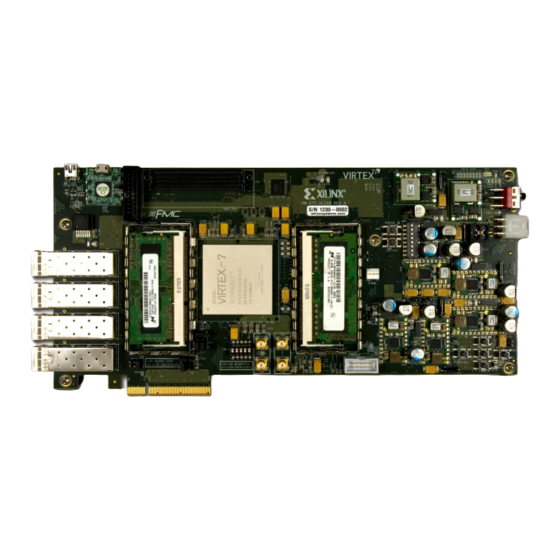
- Page 5 Xilinx VC709 Board...
- Page 6 Vivado Software Requirements Xilinx Vivado Design Suite 2015.1, Design Edition + SDK – Combined installer Note: Presentation applies to the VC709...
- Page 7 VC709 Setup Connect a USB Type- A to Micro-B cable to the USB JTAG (Digilent) connector on the VC709 board – Connect this cable to your PC – Power on the VC709 board...
- Page 8 VC709 Si5324 Setup Unzip the VC709 Si5324 Design Files (2015.1 C) ZIP file – Available through http://www.xilinx.com/vc709 Note: Presentation applies to the VC709...
- Page 9 Reducing Jitter with the Si5324...
- Page 10 Reducing Jitter with the Si5324 A means of measuring jitter is required for this section A LeCroy 816Zi-A Scope was used (stock photo shown)
- Page 11 Reducing Jitter with the Si5324 Connect SMA cables to J31 and J32, USER_SMA_CLOCK_P/N Connect these cable to your oscilloscope...
- Page 12 Reducing Jitter with the Si5324 Open a Vivado Tcl Shell: Start → All Programs → Xilinx Design Tools → Vivado 2015.1 → Vivado 2015.1 Tcl Shell Note: Presentation applies to the VC709...
- Page 13 Reducing Jitter with the Si5324 Download the “bypass” bitstream with Vivado In the Vivado Tcl Shell type: cd C:/vc709_si5324/ready_for_download source bypass_download.tcl Note: Presentation applies to the VC709...
- Page 14 Reducing Jitter with the Si5324 LeCroy Oscilloscope setup Press the Default Setup followed by the Auto Setup twice...
- Page 15 Reducing Jitter with the Si5324 Adjust the Horizontal knob until you have 5 μs/div...
- Page 16 Reducing Jitter with the Si5324 From the LeCroy scope menu, select Analysis → Serial Data…...
- Page 17 Reducing Jitter with the Si5324 Select “Quick View”...
- Page 18 Reducing Jitter with the Si5324 Set the inputs to Input1-Input2 and the Data to match your setup...
- Page 19 Reducing Jitter with the Si5324 Click the Close button...
- Page 20 Reducing Jitter with the Si5324 Note that the DCD (Duty Cycle Distortion) is 48.303 ps...
- Page 21 Reducing Jitter with the Si5324 Download the “enabled” bitstream with Vivado In the Vivado Tcl Shell type: source enabled_download.tcl Note: Presentation applies to the VC709...
- Page 22 Reducing Jitter with the Si5324 Note that the DCD (Duty Cycle Distortion) is 34.456 ps – Including the Si5324 Jitter Attenuator PLL in the clock path, reduces DCD...
- Page 23 Compile VC709 Si5324 Design...
- Page 24 Compile VC709 Si5324 Design Open Vivado Start → All Programs → Xilinx Design Tools → Vivado 2015.1 → Vivado Select Open Project Note: Presentation applies to the VC709...
- Page 25 Compile VC709 Si5324 Design Open the VC709 Design: – <Design Name>\vc709_si5324.xpr Note: Presentation applies to the VC709...
- Page 26 Compile VC709 Si5324 Design The design is fully implemented; you can recompile, or export to SDK – To recompile, right-click synth_1, select Reset Runs then Generate Bitstream Note: Presentation applies to the VC709...
- Page 27 Compile VC709 Si5324 Design Once done, both the Synthesis and Implementation will have green check marks Note: Presentation applies to the VC709...
- Page 28 Compile VC709 Si5324 Design The Si5324 Design has been implemented with IP Integrator (IPI) Click Open Block Design Note: Presentation applies to the VC709...
- Page 29 Compile VC709 Si5324 Design All the IP Blocks used in the design can be seen in this view Click Open Implemented Design Note: Presentation applies to the VC709...
- Page 30 Compile VC709 Si5324 Design View Implemented Design Note: Presentation applies to the VC709...
- Page 31 Compile VC709 Si5324 Design Select File → Export → Export Hardware Click OK Note: Presentation applies to the VC709...
- Page 32 Compile VC709 Si5324 Design Select File → Launch SDK Click OK Note: Presentation applies to the VC709...
- Page 33 Compile VC709 Software in SDK SDK Software Compile - Build ELF files in SDK – Project builds automatically Note: Presentation applies to the VC709...
- Page 34 Program VC709 with Si5324 Design...
- Page 35 Init memory with the Si5324 Application ELF – Update the bitstream (download.bit) with the Si5324 Application ELF – Cycle power on the VC709 to clear out any previous settings in the Si5324 – Select Xilinx Tools → Program FPGA (1)
- Page 36 Program VC709 with Si5324 Design Init memory with the Si5324 Application ELF – Select hello_iic_5324.elf (1) – Click Program Note: Presentation applies to the VC709...
- Page 37 Program VC709 with Si5324 Design Note that the DCD (Duty Cycle Distortion) has a low value now...
- Page 38 Program VC709 with Si5324 Design To set the Si5324 for Bypass mode edit the hello_iic_si5324.c Locate the line: // Change to 1 to set Si5324 into Bypass PLL mode Change the #if 0 to #if 1 Note: Presentation applies to the VC709...
- Page 39 Program VC709 with Si5324 Design To set the Si5324 for Bypass mode edit the hello_iic_si5324.c Scroll down and locate the line: // Change to 1 to set Si5324 Loop Bandwidth (BWSEL) Change the #if 1 to #if 0 Note: Presentation applies to the VC709...
- Page 40 Program VC709 with Si5324 Design Recompiled the ELF file – Select the hello_iic_5324 project and press F5 to rebuild Note: Presentation applies to the VC709...
- Page 41 Init memory with the Si5324 Application ELF – Update the bitstream (download.bit) with the Si5324 Application ELF – Cycle power on the VC709 to clear out any previous settings in the Si5324 – Select Xilinx Tools → Program FPGA (1)
- Page 42 Program VC709 with Si5324 Design Init memory with the Si5324 Application ELF – Select hello_iic_5324.elf (1) – Click Program Note: Presentation applies to the VC709...
- Page 43 Program VC709 with Si5324 Design Note that the DCD (Duty Cycle Distortion) is now higher...
- Page 44 References...
- Page 45 References Silicon Labs – SI5324 Data Sheet • http://www.silabs.com/Support%20Documents/TechnicalDocs/Si5324.pdf Vivado Programming and Debugging – Vivado Design Suite Programming and Debugging User Guide – UG908 • http://www.xilinx.com/support/documentation/sw_manuals/xilinx2015_1/ ug908-vivado-programming-debugging.pdf...
- Page 46 Documentation...
- Page 47 – Design Advisory Master Answer Record for Virtex-7 FPGAs • http://www.xilinx.com/support/answers/42944.htm VC709 Documentation – Virtex-7 FPGA VC709 Evaluation Kit • http://www.xilinx.com/products/boards-and-kits/dk-v7-vc709-g.html – VC709 Getting Started Guide – UG966 • http://www.xilinx.com/support/documentation/boards_and_kits/vc709/2014_3/ ug966-v7-xt-connectivity-getting-started.pdf – VC709 User Guide – UG887 • http://www.xilinx.com/support/documentation/boards_and_kits/ vc709/ug887-vc709-eval-board-v7-fpga.pdf...
Need help?
Do you have a question about the VC709 and is the answer not in the manual?
Questions and answers