Table of Contents
Advertisement
Quick Links
FEATURES
High performance, low power, narrow-band transceiver
Enhanced performance ADF7021-N with external VCO
Frequency bands using external VCO: 80 MHz to 960 MHz
Improved adjacent channel power (ACP) and adjacent
channel rejection (ACR) compared with the ADF7021-N
Programmable IF filter bandwidths: 9 kHz, 13.5 kHz,
and 18.5 kHz
Modulation schemes: 2FSK, 3FSK, 4FSK, MSK
Spectral shaping: Gaussian and raised cosine filtering
Data rates: 0.05 kbps to 24 kbps
Power supply: 2.3 V to 3.6 V
Programmable output power: −16 dBm to +13 dBm
in 63 steps
Automatic power amplifier (PA) ramp control
Receiver sensitivity
−125 dBm at 250 bps, 2FSK
−122 dBm at 1 kbps, 2FSK
Patent pending, on-chip image rejection calibration
RSET
R
LNA
LNA
RFIN
RFIN
GAIN
PA RAMP
÷1/÷2
RFOUT
BUFFER
Rev. 0
Information furnished by Analog Devices is believed to be accurate and reliable. However, no
responsibility is assumed by Analog Devices for its use, nor for any infringements of patents or other
rights of third parties that may result from its use. Specifications subject to change without notice. No
license is granted by implication or otherwise under any patent or patent rights of Analog Devices.
Trademarks and registered trademarks are the property of their respective owners.
FUNCTIONAL BLOCK DIAGRAM
TEMP
MUX
SENSOR
RSSI/
IF FILTER
LOG AMP
ADF7021-V
DIV P
N/N + 1
÷2
CP
PFD
DIV R
L2
CPOUT
Narrow-Band Transceiver IC
On-chip fractional-N PLL
On-chip, 7-bit ADC and temperature sensor
Fully automatic frequency control (AFC) loop
Digital received signal strength indication (RSSI)
Integrated Tx/Rx switch
Leakage current in power-down mode: 0.1 μA
APPLICATIONS
Narrow-band, short-range device (SRD) standards
ETSI EN 300 220
500 mW output power capability in 869 MHz g3 subband
with external PA
High performance receiver rejection, blocking, and
adjacent channel power (ACP)
FCC Part 90 (meets Emission Mask D requirements)
FCC Part 95
ARIB STD-T67
Wireless metering
Narrow-band wireless telemetry
CE
CREG[1:4]
7-BIT ADC
LDO[1:4]
2FSK
3FSK
CLOCK
4FSK
AND DATA
RECOVERY
DEMODULATOR
AGC
CONTROL
AFC
CONTROL
2FSK
Σ-Δ
3FSK
MODULATOR
4FSK
MOD CONTROL
CLK
OSC
DIV
OSC1
OSC2
CLKOUT
Figure 1.
One Technology Way, P.O. Box 9106, Norwood, MA 02062-9106, U.S.A.
Tel: 781.329.4700
Fax: 781.461.3113
High Performance,
ADF7021-V
MUXOUT
TEST MUX
TxRxCLK
Tx/Rx
TxRxDATA
CONTROL
SWD
SLE
SDATA
SERIAL
PORT
SREAD
SCLK
GAUSSIAN/
RAISED COSINE
FILTER
3FSK
ENCODING
www.analog.com
©2010 Analog Devices, Inc. All rights reserved.
Advertisement
Table of Contents

Related Manuals for Analog Devices ADF7021-V


Summary of Contents for Analog Devices ADF7021-V
-
Page 1: Features
Information furnished by Analog Devices is believed to be accurate and reliable. However, no responsibility is assumed by Analog Devices for its use, nor for any infringements of patents or other One Technology Way, P.O. Box 9106, Norwood, MA 02062-9106, U.S.A. -
Page 2: Table Of Contents
ADF7021-V TABLE OF CONTENTS Features ....................1 Demodulation, Detection, and CDR ........30 Applications ..................1 Receiver Setup ................32 Functional Block Diagram .............. 1 FSK Demodulator Optimization ..........33 Revision History ................2 AFC Operation ................ -
Page 3: General Description
The IF filter has programmable bandwidths of 9 kHz, 13.5 kHz, filtering options to improve spectral efficiency for narrow-band and 18.5 kHz. The ADF7021-V supports a wide variety of pro- applications. It is suitable for circuit applications targeted at the... -
Page 4: Specifications
ADF7021-V SPECIFICATIONS = 2.3 V to 3.6 V, GND = 0 V, T to T , unless otherwise noted. Typical specifications are at V = 3 V, T = 25°C. All measurements are performed with the EVAL-ADF7021-VDBxZ using the PN9 data sequence, unless otherwise noted. The version number of ETSI EN 300 200-1 is V2.3.1. -
Page 5: Transmission Specifications
ADF7021-V TRANSMISSION SPECIFICATIONS LBW = loop bandwidth. Table 2. Parameter Unit Test Conditions/Comments DATA RATE Limited by the loop bandwidth 2FSK 0.05 18.5 kbps LBW must be ≥1.25 × data rate for correct operation 3FSK 0.05 18.5 kbps LBW = 18.5 kHz 4FSK 0.05... -
Page 6: Receiver Specifications
ADF7021-V Parameter Unit Test Conditions/Comments 3FSK, Raised Cosine Filtering 12.5 kHz Channel Spacing 2.4 kbps PN9 data, f = 1.2 kHz 25 kHz Channel Spacing 4.8 kbps PN9 data, f = 2.4 kHz 4FSK, Raised Cosine Filtering 25 kHz Channel Spacing 11.3... - Page 7 ADF7021-V Parameter Unit Test Conditions/Comments Raised Cosine 2FSK Sensitivity at 0.25 kbps −125 = 1 kHz, high sensitivity mode, IFBW = 9.0 kHz Sensitivity at 1 kbps −121 = 1 kHz, high sensitivity mode, IFBW = 9.0 kHz Sensitivity at 2.4 kbps −120...
- Page 8 ADF7021-V Parameter Unit Test Conditions/Comments IMAGE CHANNEL REJECTION Desired signal (2FSK, 9.6 kbps, ±4 kHz deviation) is 3 dB above the sensitivity point (BER = 10 −2 ); modulated inter- ferer (2FSK, 9.6 kbps, ±4 kHz deviation) is placed at the image frequency of f −...
-
Page 9: Digital Specifications
ADF7021-V DIGITAL SPECIFICATIONS Table 4. Parameter Unit Test Conditions/Comments TIMING INFORMATION Chip Enabled to Regulator μs CREG[1:4] = 100 nF Ready Chip Enabled to Tx Mode 32-bit register write time = 50 μs TCXO Reference Depends on VCO settling XTAL... -
Page 10: General Specifications
ADF7021-V GENERAL SPECIFICATIONS Table 5. Parameter Unit Test Conditions/Comments TEMPERATURE RANGE (T −40 °C POWER SUPPLIES Voltage Supply, V All VDDx pins must be tied together 1, 2 TRANSMIT CURRENT CONSUMPTION = 3.0 V, PA is matched into 50 Ω... -
Page 11: Timing Diagrams
ADF7021-V TIMING DIAGRAMS Serial Interface SCLK DB0 (LSB) SDATA DB31 (MSB) DB30 (CONTROL BIT C3) (CONTROL BIT C2) (CONTROL BIT C1) Figure 2. Serial Interface Timing Diagram SCLK SDATA REG 7 DB0 (CONTROL BIT C1) RV16 RV15 SREAD Figure 3. Serial Interface Readback Timing Diagram 2FSK/3FSK Timing ±1 ×... - Page 12 ADF7021-V 4FSK Timing In 4FSK receive mode, MSB/LSB synchronization should be guaranteed by detection of the SWD pin in the receive bit stream. REGISTER 0 WRITE SWITCH FROM Rx TO Tx SYMBOL TxRxCLK Rx SYMBOL Rx SYMBOL Rx SYMBOL Tx SYMBOL...
- Page 13 ADF7021-V UART/SPI Mode UART mode is enabled by setting Register 0, Bit DB28 to 1. SPI mode is enabled by setting Register 0, Bit DB28 to 1 and setting Register 15, Bits[DB19:DB17] to 0x7. The transmit/receive data clock is available on the CLKOUT pin.
-
Page 14: Absolute Maximum Ratings
ADF7021-V ABSOLUTE MAXIMUM RATINGS = 25°C, unless otherwise noted. Stresses above those listed under Absolute Maximum Ratings may cause permanent damage to the device. This is a stress Table 7. rating only; functional operation of the device at these or any... -
Page 15: Pin Configuration And Function Descriptions
Signal Chain Test Pin. This pin is high impedance under normal conditions and should be left unconnected. Chip Enable. Bringing CE low puts the ADF7021-V into complete power-down. Register values are lost when CE is low, and the part must be reprogrammed after CE is brought high. - Page 16 Mnemonic Description SREAD Serial Data Output. This pin is used to feed readback data from the ADF7021-V to the microcontroller. The SCLK input is used to clock each readback bit (for example, AFC or ADC) from the SREAD pin. SCLK Serial Clock Input.
-
Page 17: Typical Performance Characteristics
ADF7021-V TYPICAL PERFORMANCE CHARACTERISTICS –80 PA_BIAS = 11µA RF FREQ = 460MHz TCXO = 19.2MHz –90 PA_BIAS = 9µA –100 PA_BIAS = 5µA –4 –110 PA_BIAS = 7µA –8 = 0.3mA –120 –12 = 0.9mA –16 –130 –20 –24 –140 –28... - Page 18 ADF7021-V RAMP RATE: TRACE = MAX HOLD DATA RATE = 9.6kbps CW ONLY PA ON/OFF RATE = 3Hz DATA = PRBS9 256 CODES/BIT PA ON/OFF CYCLES = 10,000 = 2.4kHz 128 CODES/BIT = 3.0V RF FREQ = 868MHz 64 CODES/BIT –10...
- Page 19 ADF7021-V –20 DATA RATE = 1.2kbps = 2.4Hz RSSI READBACK LEVEL RF FREQ = 868MHz –40 IFBW = 9kHz –40°C, 2.3V –40°C, 3V –60 –40°C, 3.6V +25°C, 2.3V +25°C, 3V –80 +25°C, 3.6V +85°C, 2.3V +85°C, 3V +85°C, 3.6V –100 ACTUAL RF INPUT LEVEL –120...
- Page 20 ADF7021-V –100 –70 RF FREQ = 860MHz 2FSK MODULATION 2FSK MODULATION DATA RATE = 9.6kbps –102 = 4kHz DATA RATE = 9.6kbps HIGH MIXER –80 IFBW = 12.5kHz IFBW = 25kHz LINEARITY –104 DEMOD = CORRELATOR = 3.0V –3 SENSITIVITY @ BER = 10 TEMPERATURE = 25°C...
-
Page 21: Frequency Synthesizer
A single-ended reference (TCXO, VCXO, or OCXO) can also be Loop Filter used with the ADF7021-V. This is recommended for applications The loop filter integrates the current pulses from the charge that have absolute frequency accuracy requirements of <10 ppm,... -
Page 22: Muxout
The free design tool ADIsimSRD™ Design Studio can also be The serial interface operates from a regulator supply. Therefore, used to design loop filters for the ADF7021-V. See the ADIsimSRD to write to the part, CE must be high and the regulator voltage Design Studio website (www.analog.com/adisimsrd) for details). -
Page 23: Voltage Controlled Oscillator (Vco)
The maximum VCO frequency of operation supported on the multiple of the reference and the VCO frequency. ADF7021-V is 1920 MHz, which results in a maximum RF These spurs are attenuated by the loop filter. They are more channel frequency of 960 MHz using a 2× VCO or 480 MHz noticeable on channels close to integer multiples of the reference using a 4×... -
Page 24: Transmitter
ADF7021-V TRANSMITTER RF OUTPUT STAGE DATA BITS The power amplifier (PA) of the ADF7021-V is based on a single-ended, controlled current, open-drain amplifier that has PA RAMP 0 (NO RAMP) been designed to deliver up to 13 dBm into a 50 Ω load at a PA RAMP 1 maximum frequency of 960 MHz. - Page 25 ADF7021-V Setting the Transmit Data Rate Three-Level Frequency Shift Keying (3FSK) In all modulation modes except for oversampled 2FSK mode, an In three-level FSK modulation—3FSK, also known as modified accurate clock is provided on the TxRxCLK pin to latch the data...
-
Page 26: Spectral Shaping
RF sidebands. to Register 3 in the power-up sequence for receive mode. The MSB of the first symbol should be clocked into the ADF7021-V Table 9. Three-Level Signal Mapping of the Convolutional on the first transmit clock pulse from the ADF7021-V after Encoder writing to Register 3. -
Page 27: Modulation And Filtering Options
Bits[DB10:DB8] indicated in Table 11. Normal Transmit carrier only It is important that the ADF7021-V be left in transmit mode Transmit +f tone only after the last data bit is sampled by the data clock to account for this latency. The ADF7021-V should stay in transmit mode for Transmit −f... -
Page 28: Receiver Section
If the AGC loop is disabled, the gain of the IF filter can be set to one of three levels by using the FILTER_GAIN bits (Register 9, The ADF7021-V is based on a fully integrated, low IF receiver Bits[DB23:DB22]). The filter gain is adjusted automatically if architecture. - Page 29 ADF7021-V Offset Correction Clock The total AFC settling time depends on the number of AGC gain changes during reception of a packet. A total of five gain In Register 3, the user should set the BBOS_CLK_DIVIDE bits changes gives a worst-case AGC settling time of 5 × 333 μs. To...
-
Page 30: Demodulation, Detection, And Cdr
An overview of the demodulation, detection, and clock and For 2FSK modulation, data is recovered by comparing the data recovery (CDR) of the received signal on the ADF7021-V output levels from two correlators. The performance of this is shown in Figure 46. - Page 31 ADF7021-V 2FSK Bit Slicer/Threshold Detection When used with Viterbi detection, the receiver sensitivity for 3FSK is typically 3 dB greater than that obtained using 2FSK demodulation can be implemented using the correlator threshold detection. When the Viterbi detector is enabled, FSK demodulator or the linear FSK demodulator.
-
Page 32: Receiver Setup
ADF7021-V RECEIVER SETUP Table 17. Assignment of Correlator K Value for 4FSK Register 4, Bit DB7 Register 4, Bits[DB9:DB8] Correlator Demodulator Setup Even To enable the correlator for various modulation modes, see Table 15. Linear Demodulator Setup Table 15. Enabling the Correlator Demodulator The linear demodulator can be used for 2FSK demodulation. -
Page 33: Fsk Demodulator Optimization
The remaining fields that follow the preamble do not need to The clock and data recovery for 3FSK requires a number of use dc-free coding. For these fields, the ADF7021-V can accom- parameters in Register 13 to be set (see Table 19). -
Page 34: Afc Operation
AFC OPERATION maximum AFC correction range is the difference in frequency The ADF7021-V also supports a real-time AFC loop that is between the upper and lower limits of the AFC tuning range. used to remove frequency errors due to mismatches between For example, if the maximum AFC correction range is set to the transmit and receive crystals/TCXOs. -
Page 35: Automatic Sync Word Detection (Swd)
When a valid match is identified, the external SWD pin is at the receiver input. The transmitter must transmit the sync asserted by the ADF7021-V on the next Rx clock pulse. byte MSB first, LSB last to ensure proper alignment in the This feature can be used to alert the microprocessor that a receiver sync-byte-detection hardware. -
Page 36: Applications Information
200 μs for coarse calibration and 8.2 ms for fine calibration, during measures the RSSI 10 times during the calibration. The time for an adjustment plus RSSI measurement is given by which time the ADF7021-V should not be accessed. The IF filter calibration logic requires that the IF_FILTER_DIVIDER IF_CAL_DWE... -
Page 37: Lna/Pa Matching
When calibrated, the filter center frequency can vary with changes Figure 49. ADF7021-V with Internal Tx/Rx Switch in temperature. If the ADF7021-V is used in an application where The procedure typically requires several iterations until an accept- it remains in receive mode for a considerable length of time, the able compromise is reached. -
Page 38: Image Rejection Calibration
(Register 5, Bit DB24). discrete LC pi or T-stage filter. The immunity of the ADF7021-V The magnitude of the I/Q gain is adjusted using the IR_GAIN_ to strong out-of-band interference can be improved by adding a ADJUST_MAG bits (Register 5, Bits[DB29:DB25]). -
Page 39: Packet Structure And Coding
CAL AT –40°C Table 23 lists the minimum number of writes needed to set up the ADF7021-V in either Tx or Rx mode after CE is brought = 3.0V high for a minimum of 100 μs before programming any register. - Page 40 ADF7021-V The recommended programming sequences for transmit and The difference in the power-up routine for a TCXO and XTAL receive are shown in Figure 54 and Figure 55, respectively. reference is shown in these figures. TCXO POWER-DOWN XTAL CE LOW...
- Page 41 ADF7021-V TCXO POWER-DOWN XTAL CE LOW REFERENCE REFERENCE TURN ON EXTERNAL VCO AND ALLOW ADEQUATE SETTLING CE HIGH CE HIGH WAIT 50µs + 1ms WAIT 50µs (REGULATOR POWER-UP) (REGULATOR POWER-UP + TYPICAL XTAL SETTLING) CHECK FOR REGULATOR READY CHECK FOR REGULATOR READY...
-
Page 42: Applications Circuit
AN-859 Application Note, The ADF7021-V requires very few external components for accessible from the ADF7021-V product page. Follow the refer- operation. Figure 56 shows the recommended application ence design schematic closely to ensure optimum performance circuit. -
Page 43: Serial Interface
ADF7021-V SERIAL INTERFACE The serial interface allows the user to program the 16 32-bit RSSI Readback registers using a 3-wire interface (SCLK, SDATA, and SLE). It The format of the RSSI readback word is shown in Figure 57. It consists of a level shifter, 32-bit shift register, and 16 latches. -
Page 44: Interfacing To A Microcontroller/Dsp
(RC) is coded with one quartet extending from Bit RV4 to controller using the UART mode of the ADF7021-V. To enable the Bit RV1. The product code for the ADF7021-V should read back as UART interface mode, set Bit DB28 in Register 0 high. Figure 8 PC = 0x212. -
Page 45: Register 0-N Register
ADF7021-V REGISTER 0—N REGISTER ADDRESS MUXOUT INTEGER_N FRACTIONAL_N BITS FRACTIONAL_N Tx/Rx DIVIDE RATIO TRANSMIT RECEIVE UART_MODE DISABLED ENABLED 32,764 MUXOUT 32,765 REGULATOR_READY (DEFAULT) 32,766 FILTER_CAL_COMPLETE 32,767 DIGITAL_LOCK_DETECT RSSI_READY Tx_Rx LOGIC_ZERO TRISTATE LOGIC_ONE INTEGER_N DIVIDE RATIO Figure 62. Register 0—N Register Map •... -
Page 46: Register 1-Oscillator Register
ADF7021-V REGISTER 1—OSCILLATOR REGISTER XTAL_ ADDRESS RESERVED CLKOUT_ R_COUNTER BIAS BITS DIVIDE RF R_COUNTER DIVIDE RATIO RFD1 RF_DIVIDE_BY_2 CLKOUT_ DIVIDE RATIO BUFFER_ IMPEDANCE 50Ω HIGH IMPEDANCE XTAL_ DOUBLER DISABLED ENABLED RSET = 3.6kΩ X1 XOSC_ENABLE (mA) XB2 XB1 XTAL_BIAS 20µA 25µA... -
Page 47: Register 2-Transmit Modulation Register
ADF7021-V REGISTER 2—TRANSMIT MODULATION REGISTER TxDATA_ MODULATION_ ADDRESS SCHEME INVERT Tx_FREQUENCY_DEVIATION POWER_AMPLIFIER PA_BIAS PA_RAMP BITS PA_ENABLE PA_BIAS 5µA 7µA 9µA 11µA TxDATA_INVERT PA_RAMP RATE NORMAL INVERT CLK NO RAMP INVERT DATA 256 CODES/BIT INV CLK AND DATA 128 CODES/BIT 64 CODES/BIT... -
Page 48: Register 3-Transmit/Receive Clock Register
ADF7021-V REGISTER 3—TRANSMIT/RECEIVE CLOCK REGISTER DEMOD_CLK_ ADDRESS AGC_CLK_DIVIDE SEQ_CLK_DIVIDE CDR_CLK_DIVIDE DIVIDE BITS SEQ_CLK_DIVIDE BBOS_CLK_DIVIDE DEMOD_CLK_DIVIDE AGC_CLK_DIVIDE INVALID INVALID CDR_CLK_ DIVIDE Figure 65. Register 3—Transmit/Receive Clock Register Map • • Baseband offset clock frequency (BBOS CLK) must be The sequencer clock (SEQ CLK) supplies the clock to the greater than 1 MHz and less than 2 MHz, where digital receive block. -
Page 49: Register 4-Demodulator Setup Register
ADF7021-V REGISTER 4—DEMODULATOR SETUP REGISTER DEMOD_ ADDRESS POST_DEMOD_BW DISCRIMINATOR_BW INVERT SCHEME BITS IF_FILTER _ DOT_PRODUCT IFB2 IFB1 CROSS_PRODUCT 9kHz DOT_PRODUCT 13.5kHz 18.5kHz INVALID Rx_INVERT NORMAL INVERT CLK INVERT DATA DEMOD_SCHEME INVERT CLK/DATA DW10 2FSK LINEAR DEMODULATOR POST_DEMOD_BW 2FSK CORRELATOR DEMODULATOR... -
Page 50: Register 5-If Filter Setup Register
ADF7021-V REGISTER 5—IF FILTER SETUP REGISTER IR_GAIN_ IR_PHASE_ ADDRESS ADJUST_MAG ADJUST_MAG IF_FILTER_ADJUST IF_FILTER_DIVIDER BITS CC1 IF_CAL_COARSE DISABLED ENABLED IR_PHASE_ PM2 PM1 ADJUST_MAG IF_FILTER_ IFD9 IFD6 IFD5 IFD4 IFD3 IFD2 IFD1 DIVIDER IR_PHASE_ADJUST_DIRECTION ADJUST I CH ADJUST Q CH IR_GAIN_ GM2 GM1... -
Page 51: Register 6-If Fine Calibration Setup Register
ADF7021-V REGISTER 6—IF FINE CALIBRATION SETUP REGISTER ADDRESS IF_CAL_DWELL_TIME IF_CAL_UPPER_TONE_DIVIDE IF_CAL_LOWER_TONE_DIVIDE BITS IRD1 IR_CAL_SOURCE ÷2 SOURCE ÷2 OFF SOURCE ÷2 ON IF_CAL_UPPER_ IF_FINE_CAL TONE_DIVIDE DISABLED ENABLED IR_CAL_SOURCE_ IRC2 IRC1 DRIVE_LEVEL HIGH IF_CAL_LOWER_ TONE_DIVIDE IF_CAL_ DWELL_TIME Figure 68. Register 6—IF Fine Calibration Setup Register Map •... -
Page 52: Register 7-Readback Setup Register
ADF7021-V REGISTER 7—READBACK SETUP REGISTER READBACK_ ADC_ CONTROL SELECT MODE BITS C4 (0) C3 (1) C2 (1) C1 (1) READBACK_SELECT ADC_MODE DISABLED MEASURE RSSI ENABLED BATTERY VOLTAGE TEMP SENSOR TO EXTERNAL PIN READBACK MODE AFC WORD ADC OUTPUT FILTER CAL SILICON REV Figure 69. -
Page 53: Register 8-Power-Down Test Register
ADF7021-V REGISTER 8—POWER-DOWN TEST REGISTER CONTROL BITS Rx_RESET DB15 DB14 DB13 DB12 DB11 DB10 C4 (1) C3 (0) C2 (0) C1 (0) COUNTER_RESET SYNTH_ENABLE NORMAL SYNTH OFF RESET SYNTH ON CDR_RESET NORMAL RESET DEMOD_RESET NORMAL LNA/MIXER_ENABLE RESET LNA/MIXER OFF LNA/MIXER ON... -
Page 54: Register 9-Agc Register
ADF7021-V REGISTER 9—AGC REGISTER LNA_ FILTER_ LNA_ AGC_ ADDRESS BIAS GAIN GAIN MODE AGC_HIGH_THRESHOLD AGC_LOW_THRESHOLD BITS MIXER_LINEARITY AGC_LOW_ AGC_MODE THRESHOLD DEFAULT AUTO AGC HIGH MANUAL AGC FREEZE AGC RESERVED LNA_BIAS 800µA (DEFAULT) LNA_MODE DEFAULT REDUCED GAIN AGC_HIGH_ THRESHOLD FILTER_CURRENT HIGH... -
Page 55: Register 10-Afc Register
ADF7021-V REGISTER 10—AFC REGISTER ADDRESS MAX_AFC_RANGE AFC_SCALING_FACTOR BITS AFC_EN AFC OFF AFC ON 2^15 AFC_SCALING_ MAX_AFC_RANGE FACTOR 4093 4094 4095 Figure 72. Register 10—AFC Register Map • • The AFC_SCALING_FACTOR can be expressed as When RF_DIVIDE_BY_2 (Register 1, Bit DB18) is enabled, the programmed AFC correction range is halved. -
Page 56: Register 11-Sync Word Detect Register
ADF7021-V REGISTER 11—SYNC WORD DETECT REGISTER CONTROL SYNC_BYTE_SEQUENCE BITS SYNC_BYTE_ LENGTH 12 BITS 16 BITS 20 BITS 24 BITS MATCHING_ TOLERANCE ACCEPT 0 ERRORS ACCEPT 1 ERROR ACCEPT 2 ERRORS ACCEPT 3 ERRORS Figure 73. Register 11—Sync Word Detect Register Map REGISTER 12—SWD/THRESHOLD SETUP REGISTER... -
Page 57: Register 13-3Fsk/4Fsk Demodulation Register
ADF7021-V REGISTER 13—3FSK/4FSK DEMODULATION REGISTER See the Receiver Setup section for information about programming these settings. 3FSK_PREAMBLE_ 3FSK/4FSK_ CONTROL TIME_VALIDATE 3FSK_CDR_THRESHOLD SLICER_THRESHOLD BITS 3FSK_VITERBI_ DETECTOR 3FSK_CDR_ THRESHOLD DISABLED ENABLED PHASE_ CORRECTION DISABLED ENABLED 3FSK/4FSK_SLICER_ THRESHOLD VITERBI_PATH _ MEMORY 4 BITS... -
Page 58: Register 14-Test Dac Register
ADF7021-V REGISTER 14—TEST DAC REGISTER ADDRESS TEST_DAC_GAIN TEST_DAC_OFFSET BITS ED_LEAK_FACTOR ERx PULSE_EXTENSION TEST_DAC_GAIN TEST_TDAC_EN LEAKAGE = NO PULSE EXTENSION NO GAIN TEST DAC DISABLED 2^–8 EXTENDED BY 1 × 2^1 TEST DAC ENABLED 2^–9 EXTENDED BY 2 2^–10 EXTENDED BY 3 ×... -
Page 59: Register 15-Test Mode Register
ADF7021-V REGISTER 15—TEST MODE REGISTER Σ-Δ_TEST_ ANALOG_TEST_ PLL_TEST_ PFD/CP_ Tx_TEST_ Rx_TEST_ ADDRESS MODES MODES CLK_MUX MODES MODES MODES BITS TEST_MODES CAL_OVERRIDE PFD/CP_TEST_MODES AUTO CAL DEFAULT, NO BLEED OVERRIDE GAIN (+VE) CONSTANT BLEED OVERRIDE BW (–VE) CONSTANT BLEED OVERRIDE BW AND GAIN (–VE) PULSED BLEED... -
Page 60: Outline Dimensions
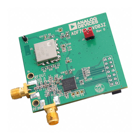
450 MHz to 470 MHz Daughter Board EVAL-ADF7021-VDB2Z 868 MHz to 870 MHz Daughter Board Z = RoHS Compliant Part. ©2010 Analog Devices, Inc. All rights reserved. Trademarks and registered trademarks are the property of their respective owners. D08635-0-4/10(0) Rev. 0 | Page 60 of 60...
Need help?
Do you have a question about the ADF7021-V and is the answer not in the manual?
Questions and answers