Table of Contents
Advertisement
Quick Links
One Technology Way • P.O. Box 9106 • Norwood, MA 02062-9106, U.S.A. • Tel: 781.329.4700 • Fax: 781.461.3113 • www.analog.com
Evaluating the
FEATURES
Full featured evaluation board for the
SPI interface for setup and control
Support LVDS output mode option
External or on-board oscillator options
Balun/transformer or amplifier input drive options
Switching power supply
VisualAnalog™ and SPIController software interfaces
EQUIPMENT NEEDED
Analog signal source and antialiasing filter
Sample clock source (if not using the on-board oscillator)
Two switching power supplies (6.0 V, 2.5 A),
CUI EPS060250UH-PHP-SZ, provided
PC running 32-bit Windows® XP, Window Vista, or Windows 7
USB 2.0 port, recommended (USB 1.1-compatible)
AD9284
evaluation board
HSC-ADC-EVALCZ FPGA-based data capture kit
SOFTWARE NEEDED
VisualAnalog
SPIController
PLEASE SEE THE LAST PAGE FOR AN IMPORTANT
WARNING AND LEGAL TERMS AND CONDITIONS.
AD9284
AD9284
TYPICAL MEASUREMENT SETUP
9284EE01
REV A
AD9284
9284EE02A
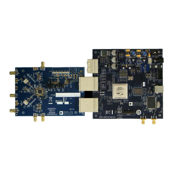
Figure 1.
AD9284
Evaluation Board and HSC-ADC-EVALCZ Data Capture Board
Rev. A | Page 1 of 24
AD9284-250EBZ User Guide
Analog-to-Digital Converter
DOCUMENTS NEEDED
AD9284
data sheet
HSC-ADC-EVALCZ data sheet
AN-905
Application Note, VisualAnalog Converter Evaluation
Tool Version 1.0 User Manual
AN-878
Application Note, High Speed ADC SPI Control Software
AN-877
Application Note, Interfacing to High Speed ADCs via SPI
AN-835
Application Note, Understanding High Speed ADC
Testing and Evaluation
GENERAL DESCRIPTION
This user guide describes the
which provides all of the support circuitry required to operate
the
AD9284
in its various modes and configurations. The
application software used to interface with the device is also
described.
The
AD9284
data sheet provides additional information and
should be consulted when using the evaluation board. All
documents and software tools are available at the
For additional information or questions, send an email to
highspeed.converters@analog.com.
HSC-ADC-EVALCZ
UG-178
AD9284
evaluation board,
FIFO
page.
Advertisement
Table of Contents

Related Manuals for Analog Devices AD9284-250EBZ


Summary of Contents for Analog Devices AD9284-250EBZ
-
Page 1: Features
AD9284-250EBZ User Guide UG-178 One Technology Way • P.O. Box 9106 • Norwood, MA 02062-9106, U.S.A. • Tel: 781.329.4700 • Fax: 781.461.3113 • www.analog.com Evaluating the AD9284 Analog-to-Digital Converter FEATURES DOCUMENTS NEEDED Full featured evaluation board for the AD9284 AD9284... -
Page 2: Table Of Contents
UG-178 AD9284-250EBZ User Guide TABLE OF CONTENTS Features ....................1 Input Signals...................3 Equipment Needed ................1 Output Signals ................3 Software Needed ................1 Default Operation and Jumper Selection Settings ....4 Documents Needed ................1 Evaluation Board Software Quick Start Procedures .....5 General Description ................. -
Page 3: Evaluation Board Hardware
AD9284. with a clean signal generator as previously specified. Typically, POWER SUPPLIES most Analog Devices evaluation boards can accept ~2.8 V p-p or This evaluation board comes with a wall-mountable switching 13 dBm sine wave input for the clock. -
Page 4: Default Operation And Jumper Selection Settings
UG-178 AD9284-250EBZ User Guide DEFAULT OPERATION AND JUMPER SELECTION RBIAS SETTINGS RBIAS has a default setting of 10 kΩ (R206) to ground and is used to set the ADC core bias current. Note that using a resistor This section explains the default and optional settings or modes value other than a 10 kΩ, 1% resistor for RBIAS may degrade... -
Page 5: Evaluation Board Software Quick Start Procedures
50 Ω terminations To change features to settings other than the default settings, and an appropriate center frequency. (Analog Devices uses click the Expand Display button, located on the bottom TTE, Allen Avionics, and K&L band-pass filters.) right corner of the window, to see what is shown in Figure 6. - Page 6 UG-178 AD9284-250EBZ User Guide Figure 6. VisualAnalog Main Window Rev. A | Page 6 of 24...
- Page 7 AD9284-250EBZ User Guide UG-178 In the ADCBase 0 tab of the SPIController window, you can Setting Up the SPIController Software access all global register settings (see Figure 9). See the AD9284 After the ADC data capture board setup is complete, set up data sheet;...
- Page 8 UG-178 AD9284-250EBZ User Guide Click the Run button in the VisualAnalog toolbar (see Troubleshooting Tips Figure 11). If the FFT plot appears abnormal, do the following: • If you see a normal noise floor when you disconnect the signal generator from the analog input, be sure you are not overdriving the ADC.
-
Page 9: Evaluation Board Schematics And Artwork
AD9284-250EBZ User Guide UG-178 EVALUATION BOARD SCHEMATICS AND ARTWORK Figure 13. Board Power Input and Supply Circuits Rev. A | Page 9 of 24... - Page 10 UG-178 AD9284-250EBZ User Guide Figure 14. DUT and Related Circuits Rev. A | Page 10 of 24...
- Page 11 AD9284-250EBZ User Guide UG-178 Figure 15. SPI Interface Circuit Rev. A | Page 11 of 24...
- Page 12 UG-178 AD9284-250EBZ User Guide Figure 16. Analog Input Circuits Rev. A | Page 12 of 24...
- Page 13 AD9284-250EBZ User Guide UG-178 Figure 17. Default Clock Path Input Circuits Rev. A | Page 13 of 24...
- Page 14 UG-178 AD9284-250EBZ User Guide 0 OHM RESISTOR NETWORK FOR LVDS MODE 47 OHM RESISTOR NETWORK FOR CMOS MODE 0 AND 47 0 AND 47 RN602 D7B_D3P O_D7B RN601 D7A_D7P O_D7A RN602 D6B_D3M O_D6B RN601 D6A_D7M O_D6A RN602 D5B_D2P O_D5B RN601...
- Page 15 AD9284-250EBZ User Guide UG-178 O_DCO_A O_DCO_B USB_SDO USB_SDI USB_CSB USB_SCLK O_D3B O_D2B O_D7B O_D6B O_D3A O_D2A O_D7A O_D6A 6469169-1 6469169-1 6469169-1 6469169-1 SDIO_DUT_1P8 SCLK_DUT_1P8 CSB_DUT_1P8 O_D1B O_D0B O_D5B O_D4B O_D1A O_D0A O_D5A O_D4A 6469169-1 6469169-1 6469169-1 6469169-1 BG10 DG10 BG10...
- Page 16 UG-178 AD9284-250EBZ User Guide Figure 20. Top Side Rev. A | Page 16 of 24...
- Page 17 AD9284-250EBZ User Guide UG-178 Figure 21. Ground Plane (Layer 2) Rev. A | Page 17 of 24...
- Page 18 UG-178 AD9284-250EBZ User Guide Figure 22. Power Plane (Layer 3) Rev. A | Page 18 of 24...
- Page 19 AD9284-250EBZ User Guide UG-178 Figure 23. Power Plane (Layer 4) Rev. A | Page 19 of 24...
- Page 20 UG-178 AD9284-250EBZ User Guide Figure 24. Ground Plane (Layer 5) Rev. A | Page 20 of 24...
- Page 21 AD9284-250EBZ User Guide UG-178 Figure 25. Bottom Side Rev. A | Page 21 of 24...
-
Page 22: Ordering Information
UG-178 AD9284-250EBZ User Guide ORDERING INFORMATION BILL OF MATERIALS Table 1. Reference Designator Description Value Manufacturer/Part No. Not applicable PCBZ 9284CE01A C101, C102, C103, C105, Ceramic, 0805, X7R capacitor 10 µF Murata/GRM21BR70J106KE76L C106, C108, C110, C111, C113, C115, C116, C125,... - Page 23 AD9284-250EBZ User Guide UG-178 Reference Designator Description Value Manufacturer/Part No. R301, R306, R307, RBIAS Precision thick film chip R0402 10 kΩ Panasonic/ERJ-2RKF1002X resistor R302, R303, R305 Film SMD 0402 resistor 1.1 kΩ Panasonic/ERJ-2GEJ112X R304, R308, R309 Precision thick film chip R0402 100 kΩ...
- Page 24 By using the evaluation board discussed herein (together with any tools, components documentation or support materials, the “Evaluation Board”), you are agreeing to be bound by the terms and conditions set forth below (“Agreement”) unless you have purchased the Evaluation Board, in which case the Analog Devices Standard Terms and Conditions of Sale shall govern. Do not use the Evaluation Board until you have read and agreed to the Agreement.
Need help?
Do you have a question about the AD9284-250EBZ and is the answer not in the manual?
Questions and answers