Table of Contents
Advertisement
Quick Links
On-Chip Debug Emulator
QB-V850MINIL, QB-V850MINI
All information contained in these materials, including products and product specifications,
represents information on the product at the time of publication and is subject to change by
Renesas Electronics Corporation without notice. Please review the latest information published
by Renesas Electronics Corporation through various means, including the Renesas Electronics
Corporation website (http://www.renesas.com).
User's Manual
Rev.4.00 Aug. 2013
Advertisement
Table of Contents

Related Manuals for Renesas QB-V850MINIL


Summary of Contents for Renesas QB-V850MINIL
- Page 1 All information contained in these materials, including products and product specifications, represents information on the product at the time of publication and is subject to change by Renesas Electronics Corporation without notice. Please review the latest information published by Renesas Electronics Corporation through various means, including the Renesas Electronics Corporation website (http://www.renesas.com).
- Page 2 Renesas Electronics products are not subject to radiation resistance design. Please be sure to implement safety measures to guard them against the possibility of physical injury, and injury or damage caused by fire in the event of the failure of a Renesas Electronics product, such as safety design for hardware and software including but not limited to redundancy, fire control and malfunction prevention, appropriate treatment for aging degradation or any other appropriate measures.
-
Page 3: Preface
Preface Preface QB-V850MINIL and QB-V850MINI are designed for use with the MCU’s made by Renesas Electronics. All components of QB-V850MINIL and QB-V850MINI are listed under “1.2 Before Using QB-V850MINIL or QB-V850MINI”. If you have any questions about QB-V850MINIL or QB-V850MINI, contact your local distributor. -
Page 4: Important
Purpose of use of the emulator: This emulator is a device to support the development of systems that uses the Renesas microcomputers. It provides support for system development in both software and hardware. The emulator is not guaranteed for use in the production line. - Page 5 (2) In no event shall Renesas Electronics Corporation be liable for any consequence arising from the use of the emulator. (3) Renesas Electronics Corporation strives to provide workarounds for and correct trouble with products malfunctions, with some free and some incurring charges.
- Page 6 (2) any other rights belonging to Renesas or to a third party. This user’s manual and the emulator are copyrighted, with all rights reserved by Renesas. This user’s manual may (3) not be copied, duplicated or reproduced, in whole or part, without prior written consent from Renesas.
-
Page 7: Safety Precautions
Safety Precautions Safety Precautions The Safety Precautions which should be taken in order to use QB-V850MINIL or QB-V850MINI safely and properly. Be sure to read and understand this document before using QB-V850MINIL or QB-V850MINI. Contact us if you have any questions about the precautions described here. - Page 8 QB-V850MINIL, QB-V850MINI Emulator Safety Precautions WARNING Warnings for AC Power Supply: Do not repair or remodel the emulator product by yourself in order to prevent danger such as an electric shock or fire and for the sake of quality assurance. For after-sale services in case of a mechanical or electrical fault, please contact your local distributor.
- Page 9 (including all accessories) is not intended for household use. After use the equipment cannot be disposed of as household waste, and the WEEE must be treated, recycled and disposed of in an environmentally sound manner. Renesas Electronics Europe GmbH can take back end of life equipment, register for this service at “http://www.renesas.eu/weee”. R20UT0221EJ0400 Rev.4.00 Page 9 of 86 2013.08.30...
-
Page 10: Table Of Contents
Outline ......................................... 15 Features ..........................................15 Before Using QB-V850MINIL or QB-V850MINI ............................16 1.2.1 Package contents ......................................16 1.2.2 Checking purpose for using QB-V850MINIL or QB-V850MINI ......................17 Supported Devices ......................................18 1.3.1 On-Chip Debug ......................................18 1.3.2 On-chip debugging with in-circuit method ..............................19 Specifications ........................................ - Page 11 System configuration when using optional products ..........................60 4.2.3 List of optional product names ...................................61 Setup Procedure ........................................62 4.3.1 Installation of software ....................................63 4.3.2 Setting of QB-V850MINIL or QB-V850MINI ............................63 4.3.3 Clock settings ......................................63 4.3.4 Switch settings......................................64 4.3.5 Mounting target connector ..................................65 4.3.6...
-
Page 12: User Registration
QB-V850MINIL, QB-V850MINI Emulator User Registration User Registration When you install debugger software, a text file for user registration is created on your PC. Fill it in and email it to your local distributor. If you have replaced an emulator main unit or emulation probe, rewrite an emulator name and serial number in the text file you filled in earlier to register your new hardware products. -
Page 13: Terminology
Some specific words used in this user's manual are defined below. Integrated development environment This tool provides powerful support for the development of embedded applications for Renesas microcomputers. It has an emulator debugger function allowing the emulator to be controlled from the host machine via an interface. - Page 14 QB-V850MINIL, QB-V850MINI Emulator Terminology V850MINIL self-check board This means the self-check board included with the QB-V850MINIL. Self-check board General term used for both the V850MINI self-check board and the V850MINIL self-check board. The symbol (#) means that the signal is active-low in this document.
-
Page 15: Outline
QB-V850MINIL, QB-V850MINI Emulator 1. Outline Outline QB-V850MINIL or QB-V850MINI is an emulator to be connected to a target device with an on-chip debug unit to efficiently debug hardware and software. Features USB connection QB-V850MINIL or QB-V850MINI can be connected to the host machine via the USB interface (1.1/2.0). -
Page 16: Before Using Qb-V850Minil Or Qb-V850Mini
1.2.1 Package contents When purchasing QB-V850MINIL or QB-V850MINI, be sure to check that all the items listed in the packing specifications are included. QB-V850MINIL or QB-V850MINI package contains the items shown below. If there are missing or damaged items, contact your local distributor. Note that the items in the QB-V850MINI package differ from those in the QB-V850MINIL package. -
Page 17: Checking Purpose For Using Qb-V850Minil Or Qb-V850Mini
Checking purpose for using QB-V850MINIL or QB-V850MINI There are mainly three purposes for using QB-V850MINIL or QB-V850MINI. The system must be configured appropriately according to each usage purpose of QB-V850MINIL or QB-V850MINI, so check the following and refer to the relevant chapter. -
Page 18: Supported Devices
QB-V850MINIL, QB-V850MINI Emulator 1. Outline Supported Devices <R> The following describes the devices that are supported by QB-V850MINIL or QB-V850MINI, as of June 2013 1.3.1 On-Chip Debug Microcontrollers supported by QB-V850MINIL or QB-V850MINI are listed in the following table. Be sure to use the latest software tools such as debuggers. -
Page 19: On-Chip Debugging With In-Circuit Method
1.3.2 On-chip debugging with in-circuit method For the following devices, on-chip debugging with the in-circuit method is possible by using QB-V850MINIL or QB-V850MINI in combination with V850MINI self-check board or debug adapter (separately available). V850MINIL self-check board is not supported to this method. -
Page 20: Specifications
QB-V850MINIL, QB-V850MINI Emulator 1. Outline Specifications This section describes QB-V850MINIL or QB-V850MINI hardware specifications and specifications for the debug function when using the Integrated debugger. Table 1-1. Hardware Specifications Classification Item Specifications <R> Note QB-V850MINIL/ Operating power supply 5 V (USB-bus powered type) 500 mA (Max.) -
Page 21: Names And Functions Of Hardware
The part names described in this chapter are used throughout this document. This chapter provides an overview of the various functions. Reading it through, the reader will gain a basic grasp of QB-V850MINIL or QB-V850MINI and the self-check board that will facilitate reading of subsequent chapters. Also check the hardware while reading this chapter: This way you may detect damage, if any, and this prevents adverse effects on the system. -
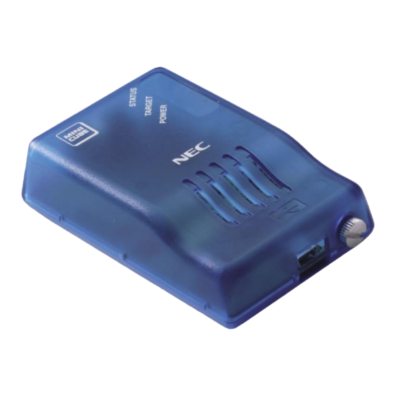
Page 22: Names Of Parts In Main Unit
QB-V850MINIL, QB-V850MINI Emulator 2. Names and functions of hardware Names of Parts in Main Unit The part names and functions of QB-V850MINIL or QB-V850MINI are described below. (a) Main unit (top view:QB-V850MINIL) (Inside the unit) OCD connector USB connector Screw... - Page 23 QB-V850MINIL, QB-V850MINI Emulator 2. Names and functions of hardware (1) SW1 Switches used for performing the initial settings for QB-V850MINIL/QB-V850MINI. They are set to OFF by default. Refer to 3.2.2 Switch settings for details on the settings. (2) USB connector A connector used for connecting the USB interface cable.
-
Page 24: Self-Check Board
2.2.1 V850MINI self-check board Figure 2-2. Part Names of V850MINI Self-Check Board (1) NWIRE1 A connector used for connecting QB-V850MINIL or QB-V850MINI (HIF3FC-20PA-2.54DSA: made by Hirose Electric Co., Ltd). (2) FW1 A connector used for connecting the flash memory programmer. -
Page 25: V850Minil Self-Check Board
µ V850ES/KJ1+ (The PD70F3318YGJ) is mounted. (7) CN1, CN2, CN3 Connectors used for connecting QB-V850MINIL or QB-V850MINI to the target system. An exchange adapter and a target connector are required separately. 2.2.2 V850MINIL self-check board Figure 2-2. Part Names of V850MINIL Self-Check Board (1) NWIRE1 A connector used for connecting QB-V850MINIL or QB-V850MINI. -
Page 26: On-Chip Debugging
3. On-Chip Debugging On-Chip Debugging This chapter describes how to use QB-V850MINIL or QB-V850MINI when performing on-chip debugging (OCD). On-chip debugging is a method to debug a microcontroller mounted on the target system. Since debugging is performed with the real device operating on the board, this method is suitable for field debugging. -
Page 27: System Configuration
• Mictor adapter: Used to connect the OCD cable to a Mictor connector. Sold separately. • Mictor connector: A connector that supports a high-speed interface. Sold separately. A debugging tool with tracing capability sold by an Renesas Electronics partner company can also be connected to this connector. -
Page 28: System Configuration In V850E2, V850E1, Or V850Es Environment
• Mictor adapter: Used to connect the OCD cable to a Mictor connector. Sold separately. • Mictor connector: A connector that supports a high-speed interface. Sold separately. A debugging tool with tracing capability sold by an Renesas Electronics partner company can also be connected to this connector. -
Page 29: Setup Procedure
See 3.2.2 Switch settings to perform setting in the correct order. Connection and startup of system Connect the host machine, QB-V850MINIL or QB-V850MINI, and target system and start the entire system. See 3.2.3 Connection and startup of system to perform setting in the correct order. -
Page 30: Installation Of Software
3.2.2 Switch settings Set SW1. SW1 is mounted inside QB-V850MINIL or QB-V850MINI main unit. Loosen the screw, open the cover, and then set SW1. Change the SW1 setting only when all the following conditions are satisfied; otherwise, use QB-V850MINIL or QB-V850MINI with the default setting (all “OFF”). -
Page 31: Connection And Startup Of System
Connecting QB-V850MINIL or QB-V850MINI to target system (1) Connect QB-V850MINIL or QB-V850MINI to the target system using the adapter and target connector. Refer to the system configuration diagrams shown in Figure 3-1 and Figure 3-2 for the adapter and target connector to be used. -
Page 32: System Shutdown
QB-V850MINIL or QB-V850MINI is lit. When using the QB-V850MINIL, if the yellow LED is on, it means that an overvoltage may be being applied. Check the target system's power supply and make sure that an appropriate voltage is being applied. -
Page 33: Designing Target System Circuits When Using V850E2S Or V850E2M
3.4.1 Example of circuit design (for V850E2S or V850E2M) Figure 3-5 illustrates an example of the design of a target system circuit that is used to connect QB-V850MINIL or QB-V850MINI. To determine the resistance value in the circuit, see the user’s manual of the target device. -
Page 34: Cautions On Target System Design (For V850E2S Or V850E2M)
QB-V850MINIL, QB-V850MINI Emulator 3. On-Chip Debugging 3.4.2 Cautions on target system design (for V850E2S or V850E2M) Note the following points when designing the target system circuits and the board. Keep the pattern length as short as possible. (1) If V is between 2.0 and 5.5 V, it is judged that target system power is being supplied, and the signals... -
Page 35: Connecting The Flmd0 Signal (For V850E2S Or V850E2M)
( a) When not performing flash self programming Connect the FLMD0 signal output from QB-V850MINIL or QB-V850MINI to the FLMD0 pin on the target device. As long as there are no problems arising from the specifications of the target device, pull the signal down to low level. - Page 36 Remark The resistance of R2 must be at least 10 times the resistance of R1. When leaving the FLMD0 signal output from QB-V850MINIL or QB-V850MINI open and connecting a port signal to FLMD0 on the target device, set the output of the port to high level in the SFR or other debugger window when writing to the flash memory during a break.
-
Page 37: Connecting The Reset# Signal (For V850E2S Or V850E2M)
To reset the target device while the target system power supply is on, connect the reset signal output from QB-V850MINIL or QB-V850MINI to the RESET# pin on the target device. The RESET# signal timing and an example connection circuit are shown below. -
Page 38: Designing Target System Circuits When Using V850E2, V850E1, Or V850Es
Target System Circuits When Using V850E2S or V850E2M. 3.5.1 Example of circuit design (for V850E2, V850E1, or V850ES) Figure 3-11 illustrates an example of the design of a target system circuit that is used to connect QB-V850MINIL or QB-V850MINI. QB-V850MINIL/... -
Page 39: Cautions On Target System Design (For V850E2, V850E1, Or V850Es)
QB-V850MINIL, QB-V850MINI Emulator 3. On-Chip Debugging 3.5.2 Cautions on target system design (for V850E2, V850E1, or V850ES) Note the following points when designing the target system circuits and the board. Keep the pattern length as short as possible. (1) If V is between 2.0 and 5.5 V, it is judged that target system power is being supplied, and the signals switch to... -
Page 40: Connecting The Flmd0 Signal (For V850E2, V850E1, Or V850Es)
( a) When not performing flash self programming Connect the FLMD0 signal output from QB-V850MINIL or QB-V850MINI to the FLMD0 pin on the target device. As long as there are no problems arising from the specifications of the target device, pull the signal down to low level. - Page 41 Remark The resistance of R2 must be at least 10 times the resistance of R1. When leaving the FLMD0 signal output from QB-V850MINIL or QB-V850MINI open and connecting a port signal to FLMD0 on the target device, set the output of the port to high level in the SFR or other debugger window when writing to the flash memory during a break.
-
Page 42: Connecting The Reset# Signal (For V850E2, V850E1, Or V850Es)
3. On-Chip Debugging 3.5.4 Connecting the RESET# signal (for V850E2, V850E1, or V850ES) This is the system reset input signal. QB-V850MINIL or QB-V850MINI controls the RESET# signal as follows. Target system power turned on Software starts up (debugger starts running))... - Page 43 QB-V850MINIL, QB-V850MINI Emulator 3. On-Chip Debugging QB-V850MINIL/ Target system QB-V850MINI 3.3 V Target device 74LVC1T45 RESET# RESET# Figure 3-16. RESET# Pin Connection Example R20UT0221EJ0400 Rev.4.00 Page 43 of 86 2013.08.30...
-
Page 44: Target Connectors For Ocd
Target Connectors for OCD A target connector for OCD must be mounted on the target system in order to connect QB-V850MINIL or QB-V850MINI to the target system. The target connector for OCD can be selected from the target connectors listed in the table below. -
Page 45: Kel Connector (For V850E2, V850E1, Or V850Es)
3.6.1 KEL connector (for V850E2, V850E1, or V850ES) A KEL connector is a target connector included with the QB-V850MINI but not with the QB-V850MINIL. Note that the KEL connector cannot be used when using the V850E2S or V850E2M. When using the KEL connector as the target connector for OCD, mount either of the following connectors on the target system. - Page 46 QB-V850MINIL, QB-V850MINI Emulator 3. On-Chip Debugging Table 3-5. KEL Connector Pin Functions (for V850E2, V850E1, or V850ES) Note 1 Pin No. Signal Name Description A1 to A6 − Connect to GND Data signal transmitted to DCU Clock for DCU DCU state transition control signal...
-
Page 47: Mictor Connector
The Mictor connector is conventionally supported as a target connector for OCD that supports the high-speed trace interface. When combining use of QB-V850MINIL or QB-V850MINI and an emulator with tracing capability sold by Renesas Eloctronics partner company, use the Mictor connector. - Page 48 QB-V850MINIL, QB-V850MINI Emulator 3. On-Chip Debugging Table 3-6. Mictor Connector Pin Functions (for V850E2S or V850E2M) Note 1 Pin No. Signal Name Description 1 and 2 − Connect to GND Clock for DCU − Power supply (The power supply for buffers of debugging interface, or...
- Page 49 3. Refer to 3.5.3 Connecting the FLMD0 signal (for V850E2, V850E1, or V850ES). 4. When the TRCCE signal (trace compression enable input) is connected as the trace interface for Renesas Electronics partner company’s emulator, the SW1 settings in QB-V850MINIL or QB-V850MINI must be changed.
-
Page 50: Sica Connector
The SICA connector is a compact target connector. Use of this connector is effective in cases such as when a mounting area cannot be secured on the target system. Note that the SICA connector may not support Renesas Electronics partner company’s emulators. - Page 51 QB-V850MINIL, QB-V850MINI Emulator 3. On-Chip Debugging Table 3-8. SICA Connector Pin Functions (for V850E2S or V850E2M) Note 1 Pin No. Signal Name Description − Connect to GND Clock for DCU − Connect to GND DCU state transition control signal −...
- Page 52 QB-V850MINIL, QB-V850MINI Emulator 3. On-Chip Debugging Table 3-9. SICA Connector Pin Functions (for V850E2, V850E1, or V850ES). Note 1 Pin No. Signal Name Description − Connect to GND Clock for DCU − Connect to GND DCU state transition control signal −...
-
Page 53: Mm Pitch 16-Pin General-Purpose Connector (For V850E2S Or V850E2M)
Note that the 2.54 mm pitch 16-pin general-purpose connector cannot be used when using the V850E2, V850E1, or V850ES. Note that the 2.54 mm pitch 16-pin general-purpose connector may not support Renesas Electronics partner company’s emulators. - Page 54 QB-V850MINIL, QB-V850MINI Emulator 3. On-Chip Debugging Table 3-10. 2.54 mm Pitch 16-pin General-Purpose Connector Pin Functions (for V850E2S or V850E2M) Note 1 Pin No. Signal Name Description − Connect to GND Note 2 RESET# System reset input signal (leave open when not used) Data signal transmitted from DCU −...
-
Page 55: 2.54 Mm Pitch 20-Pin General-Purpose Connector
A 2.54 mm pitch general-purpose connector do not need connection of adaptor. Note that 2.54 mm pitch 20-pin general-purpose connectors may not support Renesas Electronics partner company’s emulators. The followings are examples of the 2.54 mm pitch 20-pin general-purpose connector. - Page 56 QB-V850MINIL, QB-V850MINI Emulator 3. On-Chip Debugging Table 3-11. 2.54 mm Pitch General-Purpose Connector Pin Functions (for V850E2S or V850E2M) Note 1 Pin No. Signal Name Description − Connect to GND Clock for DCU − Connect to GND DCU state transition control signal −...
- Page 57 QB-V850MINIL, QB-V850MINI Emulator 3. On-Chip Debugging Table 3-12. 2.54 mm Pitch General-Purpose Connector Pin Functions (for V850E2, V850E1, V850ES) Note 1 Pin No. Signal Name Description − Connect to GND Clock for DCU − Connect to GND DCU state transition control signal −...
-
Page 58: Debugging With In-Circuit Method
By using the V850MINI self-check board included with the QB-V850MINI or the separately sold QB-V850ESKX1H-DA, QB-V850MINIL or QB-V850MINI can be used to debug the target devices shown in 4.1 below. Note that the V850MINIL self-check board included with the QB-V850MINIL cannot be used for in-circuit emulation. -
Page 59: System Configuration
The system configuration shown in the following figure illustrates the minimum system configuration required for debugging with the in-circuit method. Note that items <6> and <7> in Figure 4-1 are not included with the QB-V850MINI or QB-V850MINIL. Note also that item <5> is included with the QB-V850MINI but not with the QB-V850MINIL. -
Page 60: System Configuration When Using Optional Products
<1> Host machine: With USB ports <2> USB (accessory) <3> QB-V850MINIL or QB-V850MINI (this product) <4> OCD cable (accessory) <5> V850MINI Self-check board (accessory) (included with the QB-V850MINI) or QB-V850ESKX1H-DA <6> Check pin adapter (sold separately): An adapter used for monitoring waveforms with an oscilloscope, etc. -
Page 61: List Of Optional Product Names
List of optional product names The tables below list the optional product names. On-chip debugging is also possible for the V850ES/KJ1 or V850ES/KJ1+. The external dimensions of optional products are posted on the following Renesas Electronics webpage. URL: http://www.renesas.com/iecube/v850 Table 4-1. List of Optional Product Names (1/2) -
Page 62: Setup Procedure
Proceed to the next step if the target connector is already mounted. Connection and startup of system Connect the host machine, QB-V850MINIL or QB-V850MINI, V850MINI self-check board, and target system and start the entire system. See 4.3.6 Connection and startup of system to perform setting in the correct order. -
Page 63: Installation Of Software
4.3.2 Setting of QB-V850MINIL or QB-V850MINI Set QB-V850MINIL or QB-V850MINI to the default setting. See 3.3 Default Setting for the default settings of QB-V850MINIL or QB-V850MINI. 4.3.3 Clock settings The oscillation clock of the target device is set by the clock settings for the V850MINI self-check board. -
Page 64: Switch Settings
QB-V850MINIL, QB-V850MINI Emulator 4. Debugging with In-Circuit method 4.3.4 Switch settings For the V850MINI self-check board, two types of mode can be selected by setting SW1. Set SW1 to “Adapter” when performing emulation with the in-circuit method to set the adapter mode. -
Page 65: Mounting Target Connector
QB-V850MINIL, QB-V850MINI Emulator 4. Debugging with In-Circuit method 4.3.5 Mounting target connector Mount the target connector on the target system in the following order. Apply cream solder to the foot pattern for mounting the IC on the target system. (1)... -
Page 66: Connection And Startup Of System
Connecting QB-V850MINIL or QB-V850MINI to target system (1) Connect QB-V850MINIL or QB-V850MINI to the target system using the exchange adapter and target connector. Refer to the system configuration diagrams shown in Figures 4-1 and 4-2 for the connection of other optional products. -
Page 67: System Shutdown
(2) Turn off the power to the target system. (3) Disconnect the USB cable from the host machine. Caution If the above order is not observed, QB-V850MINIL or QB-V850MINI or the self-check board may be damaged. Default Settings (V850MINI Self-check board) Table 4-3. -
Page 68: Cautions On Using Sockets
QB-V850MINIL, QB-V850MINI Emulator 4. Debugging with In-Circuit method Cautions on Using Sockets This section describes cautions on using sockets such as the target connector and exchange adapter. The following symbols are used in this section. • TC: Target connector • EA: Exchange adapter •... -
Page 69: Recovery Of Security Id
(2) Set SW1 on the V850MINI self-check board to “Self Check”. (3) Connect the flash memory programmer to the FW1 connector on the self-check board. Caution To avoid signal conflicts, do not connect QB-V850MINIL or QB-V850MINI to the self-check board when the flash memory programmer is connected. -
Page 70: Self-Testing
5. Self-Testing Self-Testing This chapter describes how to perform self-testing of QB-V850MINIL or QB-V850MINI. When the debugger does not operate normally, this function can be used to determine whether the cause lies in QB-V850MINIL or QB-V850MINI, or in other hardware. -
Page 71: Setup Procedure
See 4.4 Default Settings for the default settings of the V850MINI self-check board. Connection and startup of system Connect the host machine, QB-V850MINIL or QB-V850MINI, and target system and start the entire system. See 5.2.4 Connection and startup of system to perform setting in the correct order. -
Page 72: Installation Of Software
(1) Connecting QB-V850MINIL or QB-V850MINI to self-check board Connect QB-V850MINIL or QB-V850MINI to the V850MINI self-check board using the OCD cable. Caution Do not connect QB-V850MINIL or QB-V850MINI to the host machine at this time. Figure 5-2. Connecting QB-V850MINIL or QB-V850MINI to Self-Check Board R20UT0221EJ0400 Rev.4.00... -
Page 73: System Shutdown
(1) Terminate the V850 JTAG OCD Checker. (2) Disconnect the USB cable from the host machine. Caution If the above order is not observed, QB-V850MINIL or QB-V850MINI or the self-check board may be damaged. R20UT0221EJ0400 Rev.4.00 Page 73 of 86... -
Page 74: Cautions
QB-V850MINIL, QB-V850MINI Emulator 6. Cautions Cautions This chapter lists cautions on using QB-V850MINIL or QB-V850MINI. Caution items are classified in the following three categories, so refer to the relevant items. [OCD] Cautions for performing on-chip debugging [IE] Cautions for performing debugging with in-circuit method... - Page 75 QB-V850MINIL or QB-V850MINI and the flash memory programmer cannot be connected at the same time. [IE] QB-V850MINIL or QB-V850MINI outputs a high-level signal to the FLMD0 pin while a program is being downloaded. (QB-V850MINIL or QB-V850MINI output becomes the high-impedance state when no program is being downloaded.) Note the FLMD0 pin connection on the target system side.
-
Page 76: Maintenance And Warranty
( d) Failure or damage attributable to fire, earthquakes, thunderbolts, floods, or other natural disasters or abnormal voltages, etc. ( e) Failure or damage attributable to modifications, repairs, adjustments, or other acts made to the product by other than Renesas Electronics Corporation. -
Page 77: Repair Provisions
QB-V850MINIL, QB-V850MINI Emulator 7. Maintenance and Warranty Repair Provisions Repairs not covered by warranty (1) Problems arising in products for which more than one year has elapsed since purchase are not covered by warranty. Replacement not covered by warranty (2)... -
Page 78: Appendix A. V850Mini Self-Check Board Circuit Diagrams
QB-V850MINIL, QB-V850MINI Emulator AppendixA. V850MINI Self-Check board circuit diagrams Appendix A. V850MINI Self-Check Board Circuit Diagrams R20UT0221EJ0400 Rev.4.00 Page 78 of 86 2013.08.30... -
Page 79: Appendix B. External Dimensions
QB-V850MINIL, QB-V850MINI Emulator AppendixB. External dimensions Appendix B. External Dimensions B.1 QB-V850MINIL, QB-V850MINI 26.1mm 84.5mm (88.5mm including screw) 56.5mm Figure B-1. QB-V850MINIL or QB-V850MINI B.2 V850MINI Self-Check Board (Unit: mm) Figure B-2. V850MINI Self-Check Board R20UT0221EJ0400 Rev.4.00 Page 79 of 86 2013.08.30... -
Page 80: Target Connectors (For Ocd)
Refer to the dimension diagrams supplied by each connector manufacturer when designing boards. The external dimension diagrams of optional products to be used for emulation with the in-circuit method are posted on the following Renesas Electronics webpage. URL: http://www.renesas.com/iecube/v850 Figure B-3. - Page 81 QB-V850MINIL, QB-V850MINI Emulator AppendixB. External dimensions Figure B-5. Mictor Connector (2-767004-2) Figure B-6. SICA Connector (SICA2P20S) R20UT0221EJ0400 Rev.4.00 Page 81 of 86 2013.08.30...
-
Page 82: Appendix C. Revision History
QB-V850MINIL, QB-V850MINI Emulator AppendixC. Revision history Appendix C. Revision History Revisions up to the previous edition are shown below. The “Applied to” column indicates the chapter in each edition to which the revision was applied. Edition Description Applied to Change of Documents Related to Development Tools (User’s Manuals) in INTRODUCTION... - Page 83 QB-V850MINIL, QB-V850MINI Emulator AppendixC. Revision history Edition Description Applied to edition Addition of V850E2S core Document whole Connection and startup of system Change of 5.2.4 CHAPTER 5 SELF-TESTING R20UT0221EJ0400 Rev.4.00 Page 83 of 86 2013.08.30...
- Page 84 On-Chip Debugger QB-V850NIMIL, QB-V850MINI User’s Manual Publication Date: Aug. 30, 2013 Rev.4.00 Published by: Renesas Electronics Corporation...
- Page 85 SALES OFFICES http://www.renesas.com Refer to "http://www.renesas.com/" for the latest and detailed information. Renesas Electronics America Inc. 2880 Scott Boulevard Santa Clara, CA 95050-2554, U.S.A. Tel: +1-408-588-6000, Fax: +1-408-588-6130 Renesas Electronics Canada Limited 1101 Nicholson Road, Newmarket, Ontario L3Y 9C3, Canada...
- Page 86 On-Chip Debugger QB-V850MINIL, QB-V850MINI User’s Manual R20UT0221EJ0400...
- Page 87 Development Software Click to view products by manufacturer: Renesas Other Similar products are found below : 1120270002 1120270003 1120270005 1120270006 1120275015 2181 2400303 2400573 2402617 2402618 2700194 2700291 2701356 2701453 2701455 2701456 2701680 2702191 2702546 2702579 2702889 2702980 2730132 2730307 2730404 2733 2981554 2985660...
Need help?
Do you have a question about the QB-V850MINIL and is the answer not in the manual?
Questions and answers