
Related Manuals for Altera Nios Cyclone II Edition


Summary of Contents for Altera Nios Cyclone II Edition
- Page 1 Nios Development Board Cyclone II Edition Reference Manual 101 Innovation Drive San Jose, CA 95134 Development Board Version 6XX-40020R www.altera.com Document Version Document Date May 2007...
- Page 2 Altera Corporation in the U.S. and other countries. All other product or service names are the property of their respective holders. Al- tera products are protected under numerous U.S.
-
Page 3: Table Of Contents
Contents About this Manual................... v How to Contact Altera ..........................v Typographic Conventions ........................vi Chapter 1. Overview Features Overview ..........................1–1 General Description ..........................1–1 Factory-Programmed Reference Design .................... 1–2 Chapter 2. Board Components Component List ............................2–1 Cyclone II EP2C35 Device (U62) ......................2–3 Push-Button Switches (SW0 - SW3) .................... - Page 4 Connecting the Ethernet Cable ......................B–1 Connecting the LCD Screen ......................B–2 Obtaining an IP Address ........................ B–2 LAN Connection ........................B–3 DHCP ............................ B–3 Static IP Address ........................B–3 Point–to–Point Connections ....................B–4 Browsing to Your Board ........................B–5 Altera Corporation...
-
Page 5: About This Manual
U3 Starting Configuration step 3 ● Improved clock circuitry figure ● Added clock signal pin tables May 2005, 1.0 First publication. How to Contact For the most up-to-date information about Altera products, refer to the following table. Altera Contact Contact Address Method Technical support Website www.altera.com/support... -
Page 6: Typographic Conventions
Non-technical support (General) Email nacomp@altera.com Email authorization@altera.com (Software Licensing) Note to table: You can also contact your local Altera sales office or sales representative. Typographic This document uses the typographic conventions shown below. Conventions Visual Cue Meaning Bold Type with Initial... - Page 7 The warning indicates information that should be read prior to starting or continuing the procedure or processes The angled arrow indicates you should press the Enter key. The feet direct you to more information on a particular topic. Altera Corporation Reference Manual May 2007 Nios Development Board Cyclone II Edition...
- Page 8 About this Manual viii Reference Manual Altera Corporation Nios Development Board Cyclone II Edition May 2007...
-
Page 9: Chapter 1. Overview
Four push-button switches connected to FPGA user I/O pins ■ Eight LEDs connected to FPGA user I/O pins ■ Dual 7-segment LED display ■ JTAG connectors to Altera devices via Altera download cables ■ 50 MHz oscillator and zero-skew clock distribution circuitry ■ Power-on reset circuitry General The Nios development board comes pre-programmed with a Nios II processor reference design. -
Page 10: Factory-Programmed Reference Design
Ethernet port. For further information on the default reference design, refer to Appendix B: Connecting to the Board via Ethernet. 1–2 Reference Manual Altera Corporation Nios Development Board Cyclone II Edition May 2007... - Page 11 Overview In the course of development, you might overwrite or erase the flash memory space containing the default reference design. Altera provides the flash image for the default reference design so you can return the board to its default state. Refer to Appendix A: Restoring the Factory Configuration for more information.
- Page 12 Overview 1–4 Reference Manual Altera Corporation Nios Development Board Cyclone II Edition May 2007...
-
Page 13: Component List
Four momentary contact switches for user input to the FPGA. D0 – D7 Individual LEDs Eight individual LEDs driven by the FPGA. U8, U9 Seven-segment LEDs Two seven-segment LEDs that display numeric output from the FPGA. Altera Corporation 2–1 May 2007... - Page 14 EPCS configuration header Connects to the EPCS serial configuration device for in-system programming. Configuration & Reset MAX Configuration controller Altera MAX EPM7256AE device used to configure the FPGA from flash memory. Serial configuration device Altera EPCS64 low-cost serial configuration device to configure the FPGA.
- Page 15 M4K Memory Blocks Total RAM Bits 483,840 Embedded 18x18 Multiplier Blocks PLLs User I/O Pins Preproduction builds of the Nios Development Board, Cyclone II Editon have an EP2C35F6728ES device. Altera Corporation Reference Manual 2–3 May 2007 Nios Development Board Cyclone II Edition...
-
Page 16: Push-Button Switches (Sw0 - Sw3)
“Configuration Controller Device (U3)” on page 2–33. For Cyclone II-related documentation including pin out data for the EP2C35 device, see the Altera Cyclone II literature page at www.altera.com/literature/lit-cyc2.jsp. Push-Button SW0 – SW3 are momentary-contact push-button switches to provide stimulus to designs in the FPGA. Refer to Figure 2–2. -
Page 17: Individual Leds (D0 - D7)
2–3. When a pin LEDs (U8 & U9) drives logic 0, the corresponding U8 and U9 LED turns on. See Table 2–5 for pin-out details. Figure 2–3. Dual Seven-Segment Display Altera Corporation Reference Manual 2–5 May 2007 Nios Development Board Cyclone II Edition... -
Page 18: Ssram Chip (U74)
FPGA so it can be used by a Nios II embedded processor as general- purpose memory. The factory-programmed Nios II reference design identifies the SSRAM devices in its address space as a contiguous 2 Mbyte, 32-bit-wide, zero-wait-state main memory. 2–6 Reference Manual Altera Corporation Nios Development Board Cyclone II Edition May 2007... - Page 19 ADSC_N ssram_adsc_n BE_n0 ssram_be_n0 BE_n1 ssram_be_n1 BE_n2 ssram_be_n2 BE_n3 ssram_be_n3 CE1_n ssram_ce1_n ssram_d0 ssram_d1 ssram_d2 ssram_d3 ssram_d4 Altera Corporation Reference Manual 2–7 May 2007 Nios Development Board Cyclone II Edition...
- Page 20 OE_n ssram_oe_n WE_n ssram_we_n ADSP_n ssram_adsp_n ADV_n ssram_adv_n ssram_ce2 CE3_n ssram_ce3_n 2–8 Reference Manual Altera Corporation Nios Development Board Cyclone II Edition May 2007...
-
Page 21: Ddr Sdram Chip (U63)
Chip (U63) SDRAM pins are connected to the FPGA as shown in Table 2–7. Altera provides a DDR SDRAM controller that allows a Nios II processor to access the DDR SDRAM device as a large, linearly-addressable memory. Table 2–7. DDR SDRAM Pin Table... - Page 22 See www.micron.com for detailed information. 2–10 Reference Manual Altera Corporation Nios Development Board Cyclone II Edition May 2007...
-
Page 23: Flash Memory (U5)
Table 2–8. Flash Memory Pin Table FPGA Pin U5 Pin Board Net Name fe_a0 fe_a1 fe_a2 fe_a3 fe_a4 fe_a5 fe_a6 fe_a7 fe_a8 fe_a9 fe_a10 fe_a11 fe_a12 fe_a13 fe_a14 Altera Corporation Reference Manual 2–11 May 2007 Nios Development Board Cyclone II Edition... - Page 24 The on-board configuration controller makes assumptions about what- resides-where in flash memory. For details refer to “SW10 – Reset, Config” on page 2–35. See www.amd.com for detailed information about the flash memory device. 2–12 Reference Manual Altera Corporation Nios Development Board Cyclone II Edition May 2007...
-
Page 25: Ethernet Mac/Phy (U4) & Rj45 Connector (Rj1)
Local Device enet_ldev_n IO Char Ready enet_iochrdy Address Strobe enet_ads_n Local Bus Clock enet_lclk Ready/Return enet_rdyrtn_n Bus Cycle enet_cycle_n Write/Read enet_w_r_n Bus Chip Select enet_datacs_n AA15 Interrupt enet_intr0 Altera Corporation Reference Manual 2–13 May 2007 Nios Development Board Cyclone II Edition... - Page 26 Data Line fe_d4 Data Line fe_d5 Data Line fe_d6 Data Line fe_d7 Data Line fe_d8 Data Line fe_d9 Data Line fe_d10 Data Line fe_d11 Data Line fe_d12 2–14 Reference Manual Altera Corporation Nios Development Board Cyclone II Edition May 2007...
-
Page 27: Serial Connector (J19)
RXD and TXD signals and visually indicate when data is being transmitted or received. Figure 6 Table 2–10 show the pin connections between the serial connectors and the FPGA. Altera Corporation Reference Manual 2–15 May 2007 Nios Development Board Cyclone II Edition... -
Page 28: Expansion Prototype Connectors (Proto1 & Proto2)
The output logic-level on the expansion prototype connector pins is 3.3V. PROTO1 switches: U19, U20, U21, U22 and U25 ● PROTO2 switches: U27, U28, U29, U30 and U31 ● 2–16 Reference Manual Altera Corporation Nios Development Board Cyclone II Edition May 2007... - Page 29 Do not connect cards to PROTO1 and CON3 at the same time. Damage to one or both cards might result. See the Altera web site for a list of available expansion daughter cards that can be used with the Nios development board at www.altera.com/devkits.
- Page 30 U2 pin 19 proto1_osc 2–18 Reference Manual Altera Corporation Nios Development Board Cyclone II Edition May 2007...
- Page 31 FPGA Pin PROTO1 Pin Connector Board Net Name proto1_pllclk proto1_clkout Figure 2–6. PROTO1 Expansion Prototype Connector - J11, J12 & J13 Pin 1 Pin 1 Pin 1 Altera Corporation Reference Manual 2–19 May 2007 Nios Development Board Cyclone II Edition...
- Page 32 Figure 2–7. PROTO1 Pin Information – J11, J12, & J13 Notes to Figure 2–7: Unregulated voltage from DC power supply. Clk from board oscillator. Clk from FPGA. Clk output from PROTO1 card to FPGA. 2–20 Reference Manual Altera Corporation Nios Development Board Cyclone II Edition May 2007...
- Page 33 AF21 proto2_io17 AE21 proto2_io18 AB20 proto2_io19 AC20 proto2_io20 AF20 proto2_io21 AE20 proto2_io22 AD19 proto2_io23 AC19 proto2_io24 AA17 proto2_io25 AA18 proto2_io26 proto2_io27 AA20 proto2_cardsel_n Altera Corporation Reference Manual 2–21 May 2007 Nios Development Board Cyclone II Edition...
- Page 34 AF17 proto2_io39 U2 pin 18 proto2_osc proto2_pllclk AF14 proto2_clkout Figure 2–8. PROTO2 Expansion Prototype Connector - J15, J16 & J17 Pin 1 Pin 1 Pin 1 2–22 Reference Manual Altera Corporation Nios Development Board Cyclone II Edition May 2007...
-
Page 35: Compactflash Connector (Con3)
CompactFlash card. Refer to Figure 2–10. The following two Connector access modes are supported: (CON3) ■ ATA (hot swappable mode) ■ IDE (IDE hard disk mode) Altera Corporation Reference Manual 2–23 May 2007 Nios Development Board Cyclone II Edition... - Page 36 Damage to one or both cards might result. Table 2–13 lists connections between CON3 and the FPGA. Table 2–13. CompactFlash Pin Table FPGA Pin CON3 Pin Pin Function Board Net Name proto1_io0 proto1_io1 2–24 Reference Manual Altera Corporation Nios Development Board Cyclone II Edition May 2007...
- Page 37 IORD_n proto1_io18 IORDY_n proto1_io19 INTRQ proto1_io22 IOCS16_n proto1_io23 proto1_io24 proto1_io25 proto1_io26 CS0_n proto1_io27 DASP proto1_io28 proto1_io29 PDIAG proto1_io30 proto1_io31 proto1_io32 proto1_io33 proto1_io34 proto1_io35 proto1_io36 proto1_io37 WE_n proto1_io38 Altera Corporation Reference Manual 2–25 May 2007 Nios Development Board Cyclone II Edition...
-
Page 38: Pmc Connector (Jh1 & Jh2)
PMC interface. Damage to either the FPGA or daughter card can result if the FPGA is not configured correctly. The factory-programmed Nios II reference design does not include a PMC interface. 2–26 Reference Manual Altera Corporation Nios Development Board Cyclone II Edition May 2007... - Page 39 PMC connector and the FPGA. Table 2–15. PMC Connector Pin Table FPGA Pin JH1 & JH2 Pin Connector Board Net Name pmc_ad0 pmc_ad1 Altera Corporation Reference Manual 2–27 May 2007 Nios Development Board Cyclone II Edition...
- Page 40 AA25 pmc_ad21 AA26 pmc_ad22 AB23 pmc_ad23 AB24 pmc_ad24 AB25 pmc_ad25 AB26 pmc_ad26 AC23 pmc_ad27 AC25 pmc_ad28 AC26 pmc_ad29 AD24 pmc_ad30 AD25 pmc_ad31 pmc_be_n0 pmc_be_n1 pmc_be_n2 pmc_be_n3 2–28 Reference Manual Altera Corporation Nios Development Board Cyclone II Edition May 2007...
-
Page 41: Mictor Connector (J25)
I/O pins and probed at J25. External scopes and logic analyzers can connect to J25 and analyze a large number of signals simultaneously. For details on Nios II debugging products that use the Mictor connector, see www.altera.com. Altera Corporation Reference Manual 2–29... - Page 42 J25 and J24 cannot be used at the same time. Figure 2–13 below shows connections from the Mictor connector to the FPGA. Figure 2–13. Mictor Connector Signaling JTAG Connector (J24) Mictor Connector FPGA (U62) (J25) 2–30 Reference Manual Altera Corporation Nios Development Board Cyclone II Edition May 2007...
-
Page 43: Test Points (Tp1 - Tp8)
TP1 – TP8 are test points connected to I/O pins on the FPGA. FPGA designs can route signals to these I/O pins to be probed. TP1 –TP8 also (TP1 – TP8) connect to the configuration controller (U3). Altera Corporation Reference Manual 2–31 May 2007... -
Page 44: Epcs64 Serial Configuration Device (U69)
EPCS device. U69 is blank by default. The Quartus II software can program FPGA configuration data (a .pof file) into U69 through an Altera download cable connected to J27. Alternately, software running on a Nios II processor design can write configuration data to U69. -
Page 45: Configuration Controller Device (U3)
Device Handbook for more information about the EPCS64 device. See the EPCS Device Controller Core with Avalon Interface chapter in the Quartus II Handbook, Volume 5: Altera Embedded Peripherals for information about the EPCS serial flash controller component in SOPC Builder. -
Page 46: Configuration & Reset Buttons
The factory-programmed Nios II reference design treats SW8 as a CPU- reset button. The Nios II reference design resets and starts executing code from its reset address when SW8 is pressed. 2–34 Reference Manual Altera Corporation Nios Development Board Cyclone II Edition May 2007... -
Page 47: Sw9 - Factory Config
When SW10 is pressed, a logic 0 is driven to the power on reset controller (U18). Refer to “Power-Supply Circuitry” on page 2–44 for more details. Whenever SW10 is pressed, the configuration controller attempts to reconfigure the FPGA. Altera Corporation Reference Manual 2–35 May 2007 Nios Development Board Cyclone II Edition... -
Page 48: Reset Distribution
The configuration controller can manage two separate FPGA configurations stored in flash memory U5. These two configurations are referred to as the factory configuration and the user configuration. A 2–36 Reference Manual Altera Corporation Nios Development Board Cyclone II Edition May 2007... -
Page 49: Configuration Process
EPCS64, and configures the FPGA with the factory configuration. SW9 provides an escape from a situation in which a valid-but-nonfunctional design is present in user flash memory or the EPCS64. Altera Corporation Reference Manual 2–37 May 2007... -
Page 50: Flash Memory Partitions
Custom FPGA designs can use the flash memory space in any way necessary. Altera recommends that you do not overwrite the factory- programmed flash memory contents. Without a valid factory configuration, the configuration controller may not be able to successfully configure the FPGA. -
Page 51: User Configuration
J24 connects to the JTAG pins (TCK, TDI, TDO, TMS, TRST) of the FPGA (U62) as shown in Figure 2–18. Altera Quartus II software can directly configure the FPGA with a new hardware image via an Altera download cable as shown in Figure 2–19. In addition, the Nios II IDE can access the Nios II processor JTAG debug module via a download cable connected to the J24 JTAG connector. - Page 52 The pins of J24 are connected directly to pins on J25, and care must be taken so that signal contention does not occur between the two connectors. 2–40 Reference Manual Altera Corporation Nios Development Board Cyclone II Edition May 2007...
-
Page 53: Jtag Connector To Epm7256Ae Device (J5)
J5 connects to the JTAG pins (TCK, TDI, TDO, TMS, TRST) of the EPM7256AE device (U3). Altera Quartus II software can perform in- system programming (ISP) to reprogram the EPM7256AE device (U3) with a new hardware image via an Altera download cable as shown in Figure 2–20. - Page 54 2–21: To use an external clock signal, remove the crystal oscillator from its socket. Make sure to note the correct orientation of the oscillator before removing it. 2–42 Reference Manual Altera Corporation Nios Development Board Cyclone II Edition May 2007...
- Page 55 The 50 MHz oscillator (Y2) is socketed and can be changed or removed by the user. To drive the clock circuitry using the external clock connector (J4), remove Y2. The factory-programmed configuration controller and Altera- provided reference designs work only with the 50 MHz clock. Altera Corporation Reference Manual 2–43...
-
Page 56: Power-Supply Circuitry
3.3V power for multiple components on the board. 5.0V power for multiple components on the board. +12V Power for the PMC connectors. -12V TP13 Power for the PMC connectors. 2–44 Reference Manual Altera Corporation Nios Development Board Cyclone II Edition May 2007... -
Page 57: Appendix A. Restoring The Factory Configuration
Flash Open a Nios II command shell. Memory On a Windows PC, click Windows Start, point to Programs, Altera, Nios II EDS <installed version>, and then click Nios II Command Shell. From the examples directory, change to the factory_recovery directory for your development kit. - Page 58 FPGA from flash memory. You should see the Factory LED turned on and activity on LEDs D0 through D7. Your board is now reconfigured to the default factory condition. A–2 Reference Manual Altera Corporation Nios Development Board Cyclone II Edition May 2007...
-
Page 59: Introduction
LAN Connection — To use your Nios development board on a LAN (for example, connecting to an Ethernet hub) do the following: Connect one end of the RJ45 cable to the Ethernet connector on the development board (RJ1). Altera Corporation B–1 May 2007... -
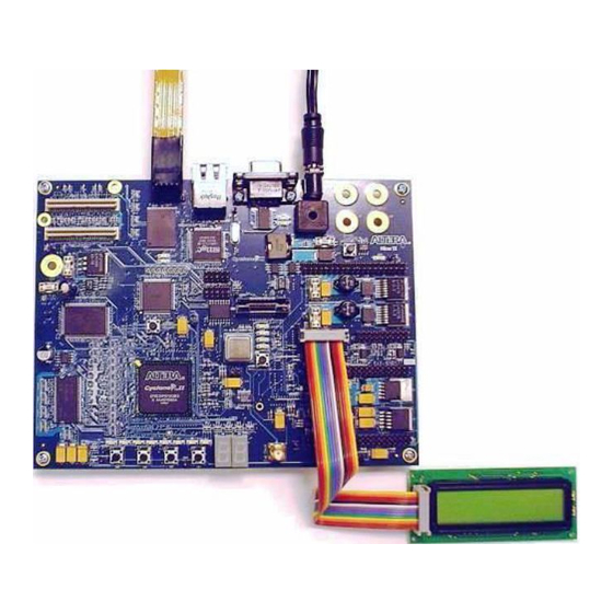
Page 60: Connecting The Lcd Screen
In order to function on a network (either LAN or point-to-point), your board must have an IP address. This section describes the methods to assign an IP address to your board. B–2 Reference Manual Altera Corporation Nios Development Board Cyclone II Edition May 2007... -
Page 61: Lan Connection
Once you know a safe IP address, you can assign it to your board using the steps below. These steps send IP configuration data to the board via an Altera JTAG download cable, such as the USB-Blaster cable. -
Page 62: Point-To-Point Connections
For example, the address 10.0.0.1 will work fine. Any address in the 10.0.0.x subnet will work, and there is no possibility of conflicting with another device on the network. After B–4 Reference Manual Altera Corporation Nios Development Board Cyclone II Edition May 2007... -
Page 63: Browsing To Your Board
IP address of the board (four numbers separated by decimal-points) as a URL directly into the browser’s Address input field. You can determine your board’s IP address by reading the messages displayed on the LCD screen. Altera Corporation Reference Manual B–5 May 2007... - Page 64 B–6 Reference Manual Altera Corporation Nios Development Board Cyclone II Edition May 2007...
Need help?
Do you have a question about the Nios Cyclone II Edition and is the answer not in the manual?
Questions and answers