
Related Manuals for Altera DE2 Board


Summary of Contents for Altera DE2 Board
- Page 1 Altera DE2 Board Development and Education Board Getting Started Guide DE2 Board Document Version 1.2 OCT. 02, 2005 by Terasic Preliminary Version © 2005 by Altera...
-
Page 2: Table Of Contents
1-1 K ................................ 1 ONTENTS 1-2 A ..........................2 SSEMBLE THE UBBER 1-3 G ................................ 3 ETTING CHAPTER 2 ALTERA DE2 BOARD ..........................4 2-1 T DE2 B ..............................4 OARD 2-2 E .............................. 4 XAMINE THE OARD 2-3 F ................................ - Page 3 Altera DE2 Board 5-1 P ............................33 OWER P THE OARD 5-2 T II ....................33 LEVEL ERILOG ODULE IN YCLONE 5-3 C ............................33 OMPILING THE ESIGN 5-4 D ............................33 OWNLOAD ITSTREAM CHAPTER 6 LAB 2: TV BOX............................33 6-1 L ..........................
-
Page 4: Chapter 1 About The Kit
The DE2 Kit provides everything you need to develop many advanced digital designs using Altera Cyclone || device. The Getting Started User Guide is written in a way to enable users to walk through many reference designs in 30 minutes. -
Page 5: Assemble The Rubber Feet
About the Kit Figure 1.1. The DE2 Kit Package Content Assemble the Rubber Feet Users can use the attached bag of copper stands, silicon feet cover, and screw to create suitable feet according to users’s own applications Assemble a screw, a copper stand, and a rubber (silicon) cover as shown in Figure 1.2 for each of the 6 screw holes on DE2. -
Page 6: Getting Help
About the Kit Figure 1.2 The Rubber Feet Set Getting Help Here are some places to get help if you encounter any problem: Email to support@terasic.com Taiwan & China: +886-3-550-8800 Korea & Japan: +82-2-512-7661... -
Page 7: Chapter 2 Altera De2 Board
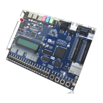
Altera DE2 Board Chapter Chapter 2 Altera DE2 Board This chapter will walk you through each part of your DE2 board to illustrate the features equipped. The DE2 Board The DE2 board is designed using the same strict design and layout practices used in high-end volume production products such as high-density PC motherboards and car infotainment systems with the highest QC standard. -
Page 8: Features
Figure 2.1. DE2 Development Board Components & Interfaces Features DE2 board provides users many features to enable various multimedia project development. Component selection was made according to the most popular design in volume production multimedia products such as DVD, VCD, and MP3 players. -
Page 9: De2 Block Diagram
Music Player, VGA and TV Labs, SD Card reader, RS-232/PS-2 Communication Labs, NIOSII, and Control Panel API DE2 Block Diagram Figure 2.2 shos a block diagram of the DE2 Board. The most recent documentation for system can be obtained from the DE2 support website at: http://de2.terasic.com... -
Page 10: De2 Block Description
With 105 M4K RAM Blocks and 483Kbit SRAM With 35 embedded multipliers and 4 PLLs Altera Serial Configuration device (EPCS16) and USB Blaster Circuit USB Blaster built in on board for programming and user API controlling JTAG Mode and AS Mode are supported... - Page 11 Altera DE2 Board With 4 push-button switches Debounced by Schimitter trigger Normal high and Generate one active-low pulse when the switch is pushed DPDT Switches Contains 18 DPDT Switches for user inputs. Clock Inputs Contains a 50MHz Oscillator Contains a 27MHz Oscillator...
- Page 12 Altera DE2 Board video devices. 10/100 Ethernet Controller Integrated MAC and PHY with a general processor interface Supports 100Base-T and 10Base-T applications. Supports full duplex operation at 10Mb/s and 100Mb/s, with auto-MDIX Fully compliant with the IEEE 802.3u Spec Supports IP/TCP/UDP checksum generation and checking...
-
Page 13: Power Up The Board To See The Demo
Switch SW17 position to OFF (down), you should hear a 1-khz sound. Switch SW17 position to ON(up) and connect the output of a MP3 player to the line-in connector of the DE2 board, you should hear the music from your headset if you play music from your MP3 player (or PC/iPod). - Page 14 Altera DE2 Board board. Your voice will be mixed with the music played from the MP3 player. Figure 2.3 The default VGA Output Pattern...
-
Page 15: Chapter 3 Using The System
3.1 describes the block diagram of the JTAG programming method. Follow the steps below to program the FPGA: Ensure the 9V power is supplied to the DE2 Board. Connect USB Cable to the USB Blaster Port of DE2. Set the Switch (SW19) to “RUN” position, as shown in Figure 3.2. -
Page 16: Configuring The Fpga In As Mode
RUN position for normal operation. Figure 3.3 shows the AS mode connection scheme. Perform the following steps to program in AS mode: Ensure the 9V power is supplied to DE2 Board. Connect USB Cable to the USB Blaster Port of DE2. -
Page 17: Controlling The De2 Using Terasic Link
Using the System Controlling the DE2 using Terasic Link We designed a special link from MAX 3128 to FPGA’s user IO pins to enable users to control the FPGA from PC using our own command set. Figure 3.4 shows the connection scheme of the Terasic Link. - Page 18 Using the System Figure 3.5 VGA Display Horizontal timing spec Both Horizontal and Vertical timing periods can be divided into four zones: H-Sync (a), back porch (b), front porch (d), and display interval(c). Refer to Figure 3.6 for detailed VGA timing spec on the four timing zones. Refer to Table 3.1 for the pin assignment of the associated interface.
- Page 19 Using the System Signal Name FPGA Pin No. Description VGA_R[0] PIN_C8 VGA Red[0] VGA_R[1] PIN_F10 VGA Red[1] VGA_R[2] PIN_G10 VGA Red[2] VGA_R[3] PIN_D9 VGA Red[3] VGA_R[4] PIN_C9 VGA Red[4] VGA_R[5] PIN_A8 VGA Red[5] VGA_R[6] PIN_H11 VGA Red[6] VGA_R[7] PIN_H12 VGA Red[7] VGA_R[8] PIN_F11 VGA Red[8]...
-
Page 20: 24-Bit Audio Codec
Microphone in, Line In, and Line Out connectors. The sample rate is adjustable from 8Khz to 96Khz by using the I2C bus on DE2 board. For detailed information on how to use the audio CODEC, users can refer to the spec under C:\DE2\Datasheet\Audio CODEC. -
Page 21: Using The Leds And Switches
There are also 18 toggle switches on the DE2 boards for users to set HIGH/LOW to the 18 GPIOs of the CycloneII FPGA. The DE2 Board has 9 green user LEDs and 18 red user LEDs. Figure 3.8 shows the related schematics. The pin assignments of the push buttons, DPDT switches, and LEDs are listed in Table 3.3, 3.4, and 3.5,... - Page 22 Using the System Figure 3.8 Push Buttons, Toggle Switches, and LEDs Signal Name FPGA Pin No. Description SW[0] PIN_N25 DPDT Switch[0] SW[1] PIN_N26 DPDT Switch[1] SW[2] PIN_P25 DPDT Switch[2] SW[3] PIN_AE14 DPDT Switch[3] SW[4] PIN_AF14 DPDT Switch[4] SW[5] PIN_AD13 DPDT Switch[5] SW[6] PIN_AC13 DPDT Switch[6]...
- Page 23 Using the System Signal Name FPGA Pin No. Description KEY[0] PIN_G26 Push Button[0] KEY[1] PIN_N23 Push Button[1] KEY[2] PIN_P23 Push Button[2] KEY[3] PIN_W26 Push Button[3] Table 3.4 Pin Assignment for Push Buttoms Signal Name FPGA Pin No. Description LEDR[0] PIN_AE23 LED Red[0] LEDR[1] PIN_AF23...
-
Page 24: Using The 7-Seg Displays And Lcd Module
Using the System Using the 7-SEG Displays and LCD Module The DE2 Board has eight 7-SEG displays and one 16x2 LCD module. The LCD module has built-in font library; users have to send control signals according to its specific timing to display desired characters at the correct location. For detailed... - Page 25 Using the System Signal Name FPGA Pin No. Description HEX0[0] PIN_AF10 Seven Segment Digital 0[0] HEX0[1] PIN_AB12 Seven Segment Digital 0[1] HEX0[2] PIN_AC12 Seven Segment Digital 0[2] HEX0[3] PIN_AD11 Seven Segment Digital 0[3] HEX0[4] PIN_AE11 Seven Segment Digital 0[4] HEX0[5] PIN_V14 Seven Segment Digital 0[5] HEX0[6]...
- Page 26 Using the System HEX5[2] PIN_P7 Seven Segment Digital 5[2] HEX5[3] PIN_T9 Seven Segment Digital 5[3] HEX5[4] PIN_R5 Seven Segment Digital 5[4] HEX5[5] PIN_R4 Seven Segment Digital 5[5] HEX5[6] PIN_R3 Seven Segment Digital 5[6] HEX6[0] PIN_R2 Seven Segment Digital 6[0] HEX6[1] PIN_P4 Seven Segment Digital 6[1] HEX6[2]...
-
Page 27: Using The Expansion Headers
Using the System Using the Expansion Headers The DE2 Board provides users two 40-pin expansion headers. Each header provides DC +5V (VCC5), DC +3.3V (VCC33), two GND pins for users to build their own daughter cards using the DE2 expansion ports. - Page 28 Using the System GPIO_0[8] PIN_F25 GPIO Connection 0[8] GPIO_0[9] PIN_F26 GPIO Connection 0[9] GPIO_0[10] PIN_N18 GPIO Connection 0[10] GPIO_0[11] PIN_P18 GPIO Connection 0[11] GPIO_0[12] PIN_G23 GPIO Connection 0[12] GPIO_0[13] PIN_G24 GPIO Connection 0[13] GPIO_0[14] PIN_K22 GPIO Connection 0[14] GPIO_0[15] PIN_G25 GPIO Connection 0[15] GPIO_0[16] PIN_H23...
-
Page 29: Using The Serial Ports(Rs232)
Table 3.8 Pin Assignment for expansion ports Using the Serial Ports(RS232) The DE2 Board uses the standard 9-pin D-SUB connector for RS-232 communications between PC and the board. The transceiver chip used is MAX232. For detailed information on how to use the chip, users can refer to the spec under C:\DE2\Datasheet\RS232. -
Page 30: Using The Serial Ports(Ps/2)
Using the Serial Ports(PS/2) 3-10 The DE2 Board offers standard PS/2 interface with a connector for a PS/2 keyboard or mouse. Figure 3.12 shows the schematic of the PS/2 connector and circuits. For how to use PS/2 mouse and keyboards, users can refer to http://www.computer-engineering.org... -
Page 31: Using The Fast Ethernet Network Controller
Using the Fast Ethernet Network Controller 3-11 The DE2 board uses DM9000A for Fast Ethernet interface. The DM9000A is a fully integrated and cost-effective low pin count single chip Fast Ethernet controller with a general processor interface, a 10/100< PHY, and 4K Dword SRAM. It is designed with low power and high performance process that support 3.3V with 5V IO... -
Page 32: Using Tv Decoder
Table 3.11 Pin Assignment for Fast Ethetnet Using TV Decoder 3-12 The DE2 Board is equipped with ADV7181 as its TV Decoder chip. The ADV7181 is integrated video decoder automatically detects and converts a standard analog baseband televison signal-compatible with worldwide standards NTSC, PAL, and SECAM into 4:2:2 component video data-compatible with 16-bit/8-bit CCIR601/CCIR656. - Page 33 Using the System Figure 3.14 TV Decoder Circuits Signal Name FPGA Pin No. Description TD_DATA[0] PIN_J9 TV Decoder Data[0] TD_DATA[1] PIN_E8 TV Decoder Data[1] TD_DATA[2] PIN_H8 TV Decoder Data[2] TD_DATA[3] PIN_H10 TV Decoder Data[3] TD_DATA[4] PIN_G9 TV Decoder Data[4] TD_DATA[5] PIN_F9 TV Decoder Data[5] TD_DATA[6]...
-
Page 34: Implementing Atv Encoder
ISP1362 under Altera NIOS II core. Please refer to Chapter 7 and Chapter 8 for details. Figure 3.15 shows the block diagram of the USB part. The pin assignment... - Page 35 Using the System Figure 3.15 USB Host and Device Circuit by ISP1362 Signal Name FPGA Pin No. Description OTG_ADDR[0] PIN_K7 ISP1362 Address[0] OTG_ADDR[1] PIN_F2 ISP1362 Address[1] OTG_DATA[0] PIN_F4 ISP1362 Data[0] OTG_DATA[1] PIN_D2 ISP1362 Data[1] OTG_DATA[2] PIN_D1 ISP1362 Data[2] OTG_DATA[3] PIN_F7 ISP1362 Data[3] OTG_DATA[4] PIN_J5...
-
Page 36: Using Irda
Table 3.13 Pin Assignment for ISP1362 Using IrDA 3-15 The DE2 Board also provides a simple wireless communication media using a 115.2Kb/s Low Power Infrared Transceiver. Please refer to the specification in C:\DE2\DataSheet\IrDA for detail information. Note that the highest transmission rate is 115.2kbit/s and both TX and RX sides have to use the same... -
Page 37: Using Sdram/Sram/Flash
3-16 Figure 3.16 shows the schematic of SDRAM, SRAM, and Flash Memory. The DE2 Board provides 8Mbyte SDRAM, 512KByte SRAM, and 1Mbyte Flash Memory. Figure 3.17 shows the schematic of the SDRAM/SRAM/Flash blocks. The pin assignments of the SDRAM, SRAM, and Flash are listed in Table 3.15,... - Page 38 Using the System Figure 3.17 SDRAM, SRAM, Flash Memory on DE2 Signal Name FPGA Pin No. Description DRAM_ADDR[0] PIN_T6 SDRAM Address[0] DRAM_ADDR[1] PIN_V4 SDRAM Address[1] DRAM_ADDR[2] PIN_V3 SDRAM Address[2] DRAM_ADDR[3] PIN_W2 SDRAM Address[3] DRAM_ADDR[4] PIN_W1 SDRAM Address[4] DRAM_ADDR[5] PIN_U6 SDRAM Address[5] DRAM_ADDR[6] PIN_U7 SDRAM Address[6]...
- Page 39 Using the System DRAM_DQ[12] PIN_AA3 SDRAM Data[12] DRAM_DQ[13] PIN_AC2 SDRAM Data[13] DRAM_DQ[14] PIN_AC1 SDRAM Data[14] DRAM_DQ[15] PIN_AA5 SDRAM Data[15] DRAM_BA_0 PIN_AE2 SDRAM Bank Address[0] DRAM_BA_1 PIN_AE3 SDRAM Bank Address[1] DRAM_LDQM PIN_AD2 SDRAM Low-byte Data Mask DRAM_UDQM PIN_Y5 SDRAM High-byte Data Mask DRAM_RAS_N PIN_AB4 SDRAM Row Address Strobe...
- Page 40 Using the System SRAM_DQ[2] PIN_AF6 SRAM Data[2] SRAM_DQ[3] PIN_AA9 SRAM Data[3] SRAM_DQ[4] PIN_AA10 SRAM Data[4] SRAM_DQ[5] PIN_AB10 SRAM Data[5] SRAM_DQ[6] PIN_AA11 SRAM Data[6] SRAM_DQ[7] PIN_Y11 SRAM Data[7] SRAM_DQ[8] PIN_AE7 SRAM Data[8] SRAM_DQ[9] PIN_AF7 SRAM Data[9] SRAM_DQ[10] PIN_AE8 SRAM Data[10] SRAM_DQ[11] PIN_AF8 SRAM Data[11] SRAM_DQ[12]...
- Page 41 Using the System FL_ADDR[15] PIN_AD16 FLASH Address[15] FL_ADDR[16] PIN_AE16 FLASH Address[16] FL_ADDR[17] PIN_AC15 FLASH Address[17] FL_ADDR[18] PIN_AB15 FLASH Address[18] FL_ADDR[19] PIN_AA15 FLASH Address[19] FL_DQ[0] PIN_AD19 FLASH Data[0] FL_DQ[1] PIN_AC19 FLASH Data[1] FL_DQ[2] PIN_AF20 FLASH Data[2] FL_DQ[3] PIN_AE20 FLASH Data[3] FL_DQ[4] PIN_AB20 FLASH Data[4] FL_DQ[5]...
-
Page 42: Chapter 4 Software Installation
Install Quartus II You need Quartus II installed on your PC to use DE2 board. Please refer to “Installing the Quartus II Software” in the Quartus II Installation & Licensing Manual for PCs, which is included on the DE2 Development Kit CD-ROM, for the software installation instructions. -
Page 43: Potential Problems And Workaround For Using Usb Blaster
Install DE2 Lab CD-ROM DE2 Lab CD-ROM contains everything you need to exercise the major parts of the DE2 Board by using many interesting labs designed and implemented by Altera and Terasic. We also implemented the DE2 Control Panel for users to... - Page 44 Software Installation control the board. Follow the steps below to install the CD-ROM Insert DE2 Lab CD-ROM into your CD-ROM drive. The menu shown in Figure 4.1 will pop up. Click on “Read Me First” and then click on “Install Software” buttons, which will install all the labs and API software into your C:\DE2.
-
Page 45: The Top Level Verilog Module And Pin Assignment
Software Installation The Top-level Verilog Module and Pin Assignment The complete top-level pin assignment is provided in C:\DE2\DE2_TOP project Please use the pin assignment in DE2_TOP project as golden pin assignment for all your projects. The top-level Verilog file is located in C:\DE2\DE2_TOP\DE2_TOP.v... -
Page 46: Chapter 5 First Lab: De2 Top-Level And Default Bitstream
The bitstream created in this Lab is used as the default bitstream loaded in DE2 board before shipping. This lab will illustrate how to compile and load the default bitstream into the DE2 Board. - Page 47 First Lab: DE2 Top-Level and Default Bitstream Figure 5.1. Menu for Opening Quartus II Project Select Quartus II project DE2_Default under C:\DE2\DE2_Default directory Please refer to Figure 5.2. Click on File Icon in the bottom of left-hand side window and select DE2_Default. Examine the file content and the IO port declaration.
-
Page 48: Lash
First Lab: DE2 Top-Level and Default Bitstream DRAM_DQ, SDRAM Data bus 16 Bits DRAM_ADDR, SDRAM Address bus 12 Bits DRAM_LDQM, SDRAM Low-byte Data Mask DRAM_UDQM, SDRAM High-byte Data Mask DRAM_WE_N, SDRAM Write Enable DRAM_CAS_N, SDRAM Column Addr Strobe DRAM_RAS_N, SDRAM Row Addr Strobe DRAM_CS_N, SDRAM Chip Select DRAM_BA_0,... -
Page 49: Link
First Lab: DE2 Top-Level and Default Bitstream OTG_INT1, ISP1362 Interrupt 1 OTG_DREQ0, ISP1362 DMA Request 0 OTG_DREQ1, ISP1362 DMA Request 1 OTG_DACK0_N, ISP1362 DMA Acknowledge 0 OTG_DACK1_N, ISP1362 DMA Acknowledge 1 //////////////////// LCD Module 16X2 //////////////// LCD_ON, LCD Power ON/OFF LCD_BLON, LCD Back Light ON/OFF LCD_RW,... - Page 50 First Lab: DE2 Top-Level and Default Bitstream VGA_SYNC, VGA SYNC VGA_R, VGA Red[9:0] VGA_G, VGA Green[9:0] VGA_B, VGA Blue[9:0] //////////// Ethernet Interface //////////////////////// ENET_DATA, DM9000A DATA bus 16Bits ENET_CMD, DM9000A Command/Data Select, 0 = Command, 1 = Data ENET_CS_N, DM9000A Chip Select ENET_WR_N, DM9000A Write ENET_RD_N,...
- Page 51 First Lab: DE2 Top-Level and Default Bitstream Compiling the Design You can click the compile button to start compilation. It will create a SOF file (DE2_Default.sof) for user to program the FPGA. To program the active serial device, you need to convert programming file to POF format.
- Page 52 Download Bitstream You can click the Programmer button to perform bitstream downloading. DE2 board uses USB-Blaster to download bitstream. We support both JTAG mode and Active Serial Programming mode (AS mode). By default, the switch is set to the position of RUN for JTAG mode so that the SOF bistream file is downloaded directly to the FPGA chip.
- Page 53 First Lab: DE2 Top-Level and Default Bitstream Figure 5.6. Hardware Setup Menu for USB-Blaster Click Close to close the Hardware Setup dialog box. In the programming window, select the desired mode (JTAG or Active Serial Programming mode). Click Add File button and select the desired SOF(for JTAG) or POF(for AS mode) accordingly.
- Page 54 HDTV/SDTV is one of the most important multimedia technologies students and engineers should learn to meet the huge industry demand in this area. In this lab, we will implement a TV box using DE2 board. Design Descriptions Figure 6.1 illustrates the block diagram of the entire design. There are two major blocks in the circuit –...
- Page 55 Connect a DVD player’s Video output to the Video IN RCA Jack of the DE2 board. Connect the VGA output of the DE2 board to a LCD/CRT Monitor. Connect the audio output of the DVD player to the line-in port of the DE2...
- Page 56 Lab 2: TV Box Figure 6.2 The Lab Setup for TV Box Important Note for the Lab DVD Player must set to the following mode: NTSC 60Hz 4:3 ratio Non-progressive mode...
-
Page 57: C Ontroller
Altera Avalon bus so that we can use NIOSII CPU to control the VGA Controller block. Once the program running on NIOS II CPU is started, the DE2 board will detect the existence of the USB mouse connected to DE2 board. Once the mouse is moved, NIOSII CPU is able to keep track the movement and record the movement in a frame buffer memory. - Page 58 NIOS II Workspace : C:\DE2\UP4_NIOS_HOST_MOUSE_VGA Refer to Figure 7.2 and setup the lab according to the following steps: Connect a USB Mouse to the USB Host Connector of the DE2 board. Connect VGA output to a LCD/CRT Monitor Load the bitstream into FPGA Run NIOS II IDE and choose C:\DE2\UP4_NIOS_HOST_MOUSE_VGA as workspace.
- Page 59 Lab 3: USB Paint Brush Figure 7.2 The Lab Setup for USB Paint Brush Application...
- Page 60 ISP1362 and its host port. Please refer to Figure First, users must use a USB A->B cable to connect the DE2 board to a USB port in the PC. Then users should execute the NIOSII software to initialize the Philips ISP1362 chip.
- Page 61 Run NIOSII IDE with DE2_ISP_1362_DC as workspace. Click on “Compile and Run” in NIOSII IDE. Connect the USB Device connector of the DE2 board to your PC using a USB cable (type A->B). A new hardware (USB device) will be found.
- Page 62 Lab 4: USB Device Execute the software: “C:\DE2\UP4_NIOS_DEVICE_LED\ ISP1362DcUsb.exe” Click on “ADD” button to increment the number/register shown on the 7-SEG displays. The incremented result is also sent back to PC side using the USB link. Click on “Clear” button to clear the register content. Figure 8.2 The Lab Setup for USB Device Application...
-
Page 63: Chapter 9 Lab 5: A Karaoke Machine
Lab 5: A Karaoke Machine Chapter Chapter 9 Lab 5: A Karaoke Machine This lab demonstrates the audio quality of the DE2 Board by using its LINEIN, LINEOUT, and microphone-in circuits in a Karaoke Machine Application implemented on the DE2 board. Design Descriptions... - Page 64 Bitstream Used: i2sound.sof or i2sound.pof Refer to Figure 9.2 and setup the lab according to the following steps: Connect a microphone to the MIC connector (pink color) of the DE2 board. Connect a MP3/IPOD/PC audio output to the LINEIN connector (blue color) of the DE2 board.
-
Page 65: Chapter 10 Lab 6: Ethernet Packet Sending/Receiving
Sending/Receiving Ethernet communication is essential to many digital products such as set-top box and home gateway. In this lab, we will show how to send and receive Ethernet packets using the Fast Ethernet controller on DE2 board. Design Descriptions 10-1 In this project, NIOS II CPU sends and receives Ethernet packets using DM9000A Ethernet PHY/MAC Controller. - Page 66 Lab 6: Ethernet Packet Sending/Receiving Figure 10.1 Packet Sending and Receiving using NIOS II CPU Lab Setup and Instructions 10-2 Project Directory: C:\DE2\UP4_NET Bitstream Used: UP4_API.sof or UP4_API.pof NIOSII Workspace: C:\DE2\UP4_NET Refer to Figure 10.2 and setup the lab according to the following steps: Plug in a CAT5 loopback cable into the Ethernet connector of DE2.
- Page 67 Lab 6: Ethernet Packet Sending/Receiving Figure 10.2 The Lab Setup for Ethernet Lab...
-
Page 68: Chapter 11 Lab 7: De2 Control Panel
Control Panel Program: C:\DE2\DE2_Control_Panel Make sure that you have C:\DE2\DE2_USB_API\HW\DE2_USB_API.sof is loaded into the FPGA. Connect your monitor and headset to the DE2 board. You should see a default Altera logo pattern on VGA and hear a 1Khz sound from your headset. - Page 69 GUI to issue commands via the USB link to the FPGA. We provide an IP to handle all the requests and perform data transferring between PC and the DE2 board. Figure 11.1. DE2 Control Panel Concept Diagram Once the DE2_Control_Panel program in C:\DE2\ is started, the user interface shown in Figure 11.2 should appear.
- Page 70 Flash memory, write one byte to the Flash, read one byte from the Flash, write a binary file to the Flash, load the content of the Flash to a file. Note The Flash memory used on DE2 board is a 1-Mbyte Flash memory organized as 1M x 8 bit.
- Page 71 Lab 7: DE2 Control Panel You need to ERASE entire Flash memory before you can write to it. Remember that the number of time a Flash memory can be erased is limited. The time required to erase entire Flash memory is 15 secs - 21 secs. Please do not close the DE2 Control Panel in the middle of operation Follow the steps to exercise the operations to the Flash memory: Click on Button Flash to change to Flash Memory Control Page (Refer to...
- Page 72 Lab 7: DE2 Control Panel Figure 11.5. Random Access to the Flash Memory You can also load a file into Flash by using Sequential Write function. Please refer to Figure 11.6. You have to specify the starting address and the length (in bytes) to be written into the Flash.
- Page 73 Lab 7: DE2 Control Panel The SDRAM / SRAM Controller and Programmer 11-4 The DE2 Control Panel can serves as a SDRAM Programmer. Users can read/write a 16-bit word from/to the SDRAM, write a binary file to the SDRAM, load the content of the SDRAM to a file. DE2 Control Panel can also controls SRAM using the identical method.
- Page 74 Lab 7: DE2 Control Panel Figure 11.8. The SDRAM Controller Panel PS/2 and 7-SEG Display Control 11-5 DE2 Control Panel gives you a control window with associated IP to allow users to input using PS/2 keyboard; the keys pressed on the keyboard will be displayed in the message box of the DE2 Control Panel.
- Page 75 Lab 7: DE2 Control Panel Figure 11.9 PS2 and USB/RS232 connection Setup Figure 11.10 DE2 Control Panel – PS/2 Keyboard message box TOOLS - Multi-Port SRAM/SDRAM/Flash Controller 11-6 To let users/students implement and test their IP cores without requiring them to implement complex API/Host control software and memory (SRAM/SDRAM/Flash) controllers, we provide users an integrated control environment consisting of software controller in C++, USB command controller,...
- Page 76 Lab 7: DE2 Control Panel SRAM/SDRAM/Flash. Once the content is downloaded to the SDRAM/Flash, users can configure the memory controllers so that their IP can read/write the SDRAM/Flash via the asynchronous ports connected. Repeat the following steps to exercise the multi-port Flash controller – we will implement a Flash Music Player as example here.
- Page 77 Make sure the checkboxes of Default Image and Cursor Enable are checked. Connect your VGA monitor to the DE2 board and you should see the default image shown on the VGA screen with a green cursor which can be controlled by moving the X/Y-axis scrolling bars of the default image shown on the DE2 Control Panel (VGA page).
- Page 78 Lab 7: DE2 Control Panel users’ own image data. Figure 11.13 Display default image and use the scrolling bars to control cursor moving VGA Display Control Panel – Display User’s Own Image 11-8 DE2 Control Panel can display users’ own images on VGA monitors. Repeat the following steps to display users’...
- Page 79 SRAM can be displayed on a VGA monitor Switch to VGA Page and deselect the checkbox of Default Image. You should see the VGA monitor connected to the DE2 board is showing the Raw_Data_Gray stored in SRAM, as shown in Figure 11.15. Users can turn off the green cursor by deselecting the checkbox of Cursor Enable.
- Page 80 This section describes how to prepare users’ own image files to be loaded into the external SRAM or internal M4K SRAM and displayed on the monitor connected to the DE2 board. Use any image processing tools such as Corel Photo Paint to load your desired image data.
-
Page 81: Ester
Lab 7: DE2 Control Panel TXT format) for the black&white version of the image – the threshold for judging black or white level is defined in the BW Threshold. Image Source R/G/B Band B&W Output Result Filter Threshold (640x480) Filter Color Picture R/G/B Raw_Data_Gray... - Page 82 SD card or CF card, to store music/movie files; many new commercial audio/media players have very high-end audio DAC circuits to provide users’ the best sound quality. The DE2 board provides users the hardware and software platform for SD card access and professional audio performance so that many multimedia products can be designed using the DE2 board.
-
Page 83: I Nstructions
Load the bitstream into FPGA Run NIOSII IDE under the workspace C:\DE2\UP4_SD_Card_Audio Connect your headset of speaker to the DE2 board and you should hear professional audio quality of the music files stored in the SD Card. Note that the music files must be in WAV format. - Page 84 Lab 8: SD Card Music Player Figure 12.2 The Lab Setup for SD Card Music Player Lab...
-
Page 85: Revision History
Schematic 13-2 Please send email to support@terasic.com for requesting schematic information. Always Visit DE2 Webpage for New Labs 13-3 We will be continuing providing interesting examples and labs on our DE2 www.altera.com or de2.terasic.com webpage. Please visit for more information.
Need help?
Do you have a question about the DE2 Board and is the answer not in the manual?
Questions and answers