Table of Contents
Advertisement
Quick Links
Open-Q™ 670 HDK Hardware Development Kit
User Guide
[Document: ITC-01CGS1394-UG-001 Version: 1.0]
Your use of this document is subject to and governed by those terms and conditions in the Intrinsyc Purchase an Open-Q™ 670 HDK Hardware
Development Kit and Software License Agreement for the Open-Q 670 Hardware Development Kit, which you or the legal entity you represent,
as the case may be, accepted and agreed to when purchasing an Open-Q Development Kit from Intrinsyc Technologies Corporation
("Agreement").
You may use this document, which shall be considered part of the defined term "Documentation" for purposes of the
Agreement, solely in support of your permitted use of the Open-Q 670 Hardware Development Kit under the Agreement. Distribution of this
document is strictly prohibited without the express written permission of Intrinsyc Technologies Corporation and its respective licensors, which
they can withhold, condition or delay in its sole discretion.
Intrinsyc is a trademark of Intrinsyc Technologies Corporation., registered in Canada and other countries.
Qualcomm® and Snapdragon™ are trademarks of Qualcomm® Incorporated, registered in the United States and other countries. Other
product and brand names used herein may be trademarks or registered trademarks of their respective owners.
This document contains technical data that may be subject to U.S. and international export, re-export, or transfer ("export") laws. Diversion
contrary to U.S. and international law is strictly prohibited.
Advertisement
Table of Contents

Related Manuals for Intrinsyc Open-Q 670 HDK


Summary of Contents for Intrinsyc Open-Q 670 HDK
- Page 1 [Document: ITC-01CGS1394-UG-001 Version: 1.0] Your use of this document is subject to and governed by those terms and conditions in the Intrinsyc Purchase an Open-Q™ 670 HDK Hardware Development Kit and Software License Agreement for the Open-Q 670 Hardware Development Kit, which you or the legal entity you represent, as the case may be, accepted and agreed to when purchasing an Open-Q Development Kit from Intrinsyc Technologies Corporation (“Agreement”).
- Page 2 Open-Q™ 670 HDK Hardware Development Kit User Guide Version 1.0 IDENTIFICATION Document Title Open-Q™ 670 HDK Hardware Development Kit User Guide Document Number ITC-01CGS1394-UG-001 Version Date December 10, 2018 Revision History REVISION DATE DESCRIPTION PAGES December 10, 2018 Initial Draft, from 80-PJ602-2_B_HDK670(SDA670) Copyright Intrinsyc Technologies Corporation...
-
Page 3: Table Of Contents
Development Platform Notice ..............7 Anti-Static Handling Procedures ............7 Kit Contents....................8 Hardware Identification Label..............9 System Block Diagram ................10 Open-Q 670 HDK Processor Board ............ 11 3.7.1 Processor Board Mechanical Properties............12 3.7.2 Processor Board Block Diagram ................ 12 3.7.3... -
Page 4: Introduction
• Configuration • Processor board • Carrier Board • Display Board for LCD 1.3 Intended Audience This document is intended for users who would like to develop custom applications on the Intrinsyc Open-Q 670 Hardware Development Kit. Copyright Intrinsyc Technologies Corporation... -
Page 5: Documents
2. DOCUMENTS This section lists the supplementary documents for the Open-Q 670 Hardware Development Kit. 2.1 Applicable Documents REFERENCE TITLE Intrinsyc Purchase and Software License Agreement for the Open-Q Development Kit 2.2 Reference Documents REFERENCE TITLE 2.3 Terms and Acronyms... -
Page 6: List Of Figures
Figure 3-1 HDK670 Platform Top ......................8 Figure 3-2 Assembled Open-Q 670 Hardware Development Kit bottom ..........9 Figure 3-3 Open-Q 670 HDK Processor board + Carrier Board Block Diagram ........10 Figure 3-4 Open-Q 670 HDK PROCESSOR BOARD ................11 Figure 3-5 Open-Q 670 Processor Board Block Diagram .............. -
Page 7: Open-Q 670 Hardware Development Kit
The Open-Q 670 Hardware Development Kit has exposed electronics and chipsets. Proper anti-static precautions should be employed when handling the kit, including but not limited to: • Using a grounded anti-static mat • Using a grounded wrist or foot strap Copyright Intrinsyc Technologies Corporation... -
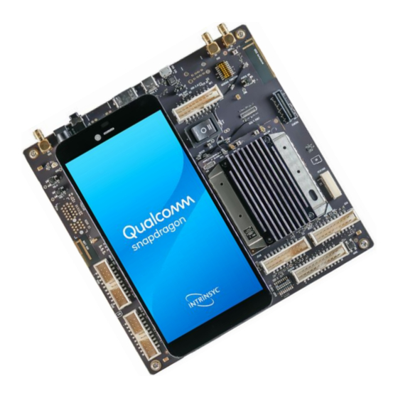
Page 8: Kit Contents
Mini-ITX form-factor carrier board for I/O and connecting with external peripherals o 12V power adapter o USB type-C cable and charger o 5.65” (1440x2160) Display card o Lithium ion battery 4.4V/3000mAh Figure 3-1 HDK670 Platform Top Copyright Intrinsyc Technologies Corporation... -
Page 9: Hardware Identification Label
Open-Q™ 670 HDK Hardware Development Kit User Guide Version 1.0 Figure 3-2 Assembled Open-Q 670 Hardware Development Kit bottom The development kit comes with Android software pre-programmed on the CPU board or processor board. Please contact Intrinsyc for availability of camera modules, sensor boards, and other accessories: sales@intrinsyc.com 3.5 Hardware Identification Label... -
Page 10: System Block Diagram
Type C USB3.1+DP JTAG JTAG USB1_SS JTAG expansion USB_HS JTAG GPIO General Config(S2302) USB to UART Micro B UART QUP12 Bridge GPIO Boot Config(S2301) Figure 3-3 Open-Q 670 HDK Processor board + Carrier Board Block Diagram Copyright Intrinsyc Technologies Corporation... -
Page 11: Open-Q 670 Hdk Processor Board
• PMIC: PM670 + PM670L – PMIC for Peripheral LDOs, Boost Regulators • SMB1355 Parallel charger • WCN3990 Atheros Wi-Fi + BT +FM combo chip over SLIMbus, Analog IQ, UART, PCM • WCD9341 Audio Code • SDR660 GNSS support Figure 3-4 Open-Q 670 HDK PROCESSOR BOARD Copyright Intrinsyc Technologies Corporation... -
Page 12: Processor Board Mechanical Properties
3.7.2 Processor Board Block Diagram The Open-Q 670 HDK Processor board measuring 60mm x 70mm is where all the processing occurs. It is connected to the carrier via two 240-pin high speed board-to-board connector. The purpose of the connectors is to bring out essential signals such that other peripherals can interface with the platform. - Page 13 2x16bit 6Gbps per lane eMMC SDC1 QLINK QLINK(1Tx/3Rx) WWAN eMCP eMCP (SDR660) RFFE1 clk/data 4bit eMMC5.1 SDC2 USB3.1+DP USB0_SS JTAG JTAG USB1_SS USB_HS JTAG GPIO UART QUP12 GPIO Figure 3-5 Open-Q 670 Processor Board Block Diagram Copyright Intrinsyc Technologies Corporation...
-
Page 14: Hardware Specification
Open-Q™ 670 HDK Hardware Development Kit User Guide Version 1.0 3.7.3 Hardware Specification Table 3.7-2 Open-Q 670 HDK Processor Board Hardware Features Subsystem / Feature Set Description Specification Connectors Qualcomm® Snapdragon™ 670 Chipset SDA670 A customized 64-bit ARM Processor v-8 compliant applications processor (Qualcomm®... - Page 15 100-pin display Connector MIPI D-PHY Specification v0.65, v0.81, v0.90, v1.01 ,v1.2 1 x Type-C USB 3.1 Type-C USB 3.1 USB3.1 Connectors 2 x 240pin BB Card Connector for BB Card 2 x 240 pin B2B connector connector Copyright Intrinsyc Technologies Corporation...
-
Page 16: Open-Q 670 Hdk Carrier Board
Open-Q™ 670 HDK Hardware Development Kit User Guide Version 1.0 3.8 Open-Q 670 HDK Carrier Board The Open-Q 670 HDK Carrier board is a Mini-ITX form factor board with various connectors used for connecting different peripherals. The following are the mechanical properties of the carrier board: Table 3.8-1 Open-Q 670 HDK Carrier Board Mechanical Properties... -
Page 17: Dip Switch Configuration Options
Open-Q™ 670 HDK Hardware Development Kit User Guide Version 1.0 3.8.1 Dip switch Configuration Options There is a DIP switch S2301 on the south top side of the Open-Q 670 HDK carrier board. The 8-bit switch allows the user to control the system configuration and boot options. Table 3.8-1 below outlines the pin outs and connections of this DIP switch. - Page 18 OFF Note: SSC SPI2 is routed to QUP_TP by default Warning! : Before making any changes to the dip switch, make sure to note down the previous configuration. The default switch settings are above. Copyright Intrinsyc Technologies Corporation...
-
Page 19: Carrier Board Expansion Connectors
For earpiece output expansion header after signal has Supported by WCD9341 been processed USB 3.1 USB 3.1 Type-C header Transfer data to and from CPU 2.4 – 5 GHz WLAN Antenna 2X PCB Antenna Antenna to BB card Copyright Intrinsyc Technologies Corporation... - Page 20 The information listed below is of particular use for those who want to interface other external hardware devices with the Open-Q 670 HDK. Before connecting anything to the development kit, please ensure the device meets the specific hardware requirements of the processor.
-
Page 21: Power Options
Figure 3-8 J2103 3.3V TTL Debug UART The header consists of TX, RX and GND pins. It is a 3.3V TTL UART header. To get the serial terminal working with a PC, the following cable (or similar) is needed http://www.digikey.ca/product-detail/en/TTL-232R-RPI/768-1204-ND/4382044 Copyright Intrinsyc Technologies Corporation... -
Page 22: Debug Serial Uart Over Usb J2102
This connector provides a JTAG interface to the main processor by which users can connect a JTAG (Lauterbach / USB Wiggler) 20 pin ARM JTAG. NOTE: The development kit does not include software support for JTAG Copyright Intrinsyc Technologies Corporation... -
Page 23: Sensor Io Expansion Header J2501
If user application does not require a sensor, then this header can be used for other applications that require I2C or GPIO input and output connections. Following is the pin breakout for sensor expansion header J2501 Copyright Intrinsyc Technologies Corporation... -
Page 24: Nfc Expansion Header J2401
In summary, if sensor application is not needed, this expansion header can provide SSC SPI1 and I2C. Please refer to the schematic and consider the power before connecting anything to this header. 3.8.2.6 NFC Expansion Header J2401 Figure 3-12 J2401 NFC EXPANSION HEADER Copyright Intrinsyc Technologies Corporation... -
Page 25: Headset Jack J1501
In general, if there is no need for NFC application, this expansion header can provide two GPIOs, I2C, free running clocks, and enable voltage/ power source to external peripherals. 3.8.2.7 Headset Jack J1501 Figure 3-13 HEADPHONE JACK Copyright Intrinsyc Technologies Corporation... -
Page 26: Audio Inputs Expansion Header J1601
This header expansion provides the following audio inputs: 3 digital mics ◼ 3 analog mics ◼ Voltage rails to support analog and digital mics ◼ The table below outlines the pin out information of the audio inputs expansion header J1601: Copyright Intrinsyc Technologies Corporation... -
Page 27: Audio Outputs Expansion Header J1602
1 differential analog earpiece amplifier output (no external amp needed) ◼ 2 speaker amplifier enable control ◼ Voltage rails to support analog and digital mics ◼ The table below outlines the pin out information of the audio outputs expansion header J1602: Copyright Intrinsyc Technologies Corporation... -
Page 28: Usb3.1 Type-C Connector J1201
The HDK carrier board has two on-board PCB antennas that connects to the WCN3990 WiFi module on the processor board via coaxial cables that attaches to MH4L receptacles. These antennas connect to the processor board in the following configuration: Copyright Intrinsyc Technologies Corporation... -
Page 29: On Board Pcb Gnss Antenna
0ohm jumpers for user to use an external GNSS antenna via the SMA connector. The option pads are between the antenna and the eLNA input. Copyright Intrinsyc Technologies Corporation... -
Page 30: Gnss Sma Connector J3802
Self-regulated camera modules can be powered with 3.3V power (MB_VREG_3P3) ◼ Uses Amphenol 11826-ACA connector for exposing MIPI, MCLK, CCI, GPIOs and ◼ Power rails. Please use Amphenol 11828-1CA mating connector to access these signals. ◼ Copyright Intrinsyc Technologies Corporation... - Page 31 FLASHLED3 FLASH_R3LED_EN PMI8998 GPIO3 DGND DGND MIPI_CSI2_LANE3_N CSI2 data FLASH_FRONT_EN SDA GPIO21 CSI2 data SDA GPIO22 MIPI_CSI2_LANE3_P FL_STROBE_TRIG DGND DGND CSI2 data 1.8V power MIPI_CSI2_LANE2_N P1V8_CAM_IOVDD supplier MIPI_CSI2_LANE2_P CSI2 data P1V2_DVDD_CAM1_2 1.2V power supplier DGND DGND Copyright Intrinsyc Technologies Corporation...
- Page 32 CSI0 clock DGND DGND LASER_IRQ SDA GPIO26 MIPI_CSI1_LANE3_N CSI1 data LASER_CE SDA GPIO100 MIPI_CSI1_LANE3_P CSI1 data DGND DGND CSI1 data P2V8_CAMA3 MIPI_CSI1_LANE2_N 2.8V power supplier CSI1 data P2V8_VCM_LASER_ MIPI_CSI1_LANE2_P DGND DGND SDA GPIO24 CSI1 data CAM_IRQ MIPI_CSI1_LANE1_N Copyright Intrinsyc Technologies Corporation...
- Page 33 CSI 2 Up to 1 lane 3D 1 lane 3D use case / Dual 1 lane configuration CSI0 + CSI1 + CSI2 Up to 4 lane Three 4-lane CSI (4+4+4 or 4+4+2+1) CPHY Three 3-trio CPHY1.0 Copyright Intrinsyc Technologies Corporation...
-
Page 34: Vertigo Sensor Connector
HDMI monitor/ television via an HDMI cable. The HDK supports HDMI output up to 1920x1080. The LT9611 MIPI DSI to HDMI1.4 bridge IC itself features a resolution up to 4K30Hz. Figure 3-22 HDMI Connector (J1401) Copyright Intrinsyc Technologies Corporation... - Page 35 (off = display; on=HDMI) Figure 3-23 Dip Switch S2301-8 See Table 3.8-2 Dip Switch S2301 HW / SW configuration for more details. To disable UEFI display before using HDMI, run the following command: fastboot oem select-display-panel none Copyright Intrinsyc Technologies Corporation...
-
Page 36: Display Card
Can support external backlight driver control and power – PM670 Triple supply topology for TFT display panels – The development platform can support the following display combination MIPI DSI 1 x 4lane DSI0 Support up to FHD+ (2160 x 1440) at 60fps Copyright Intrinsyc Technologies Corporation... -
Page 37: Display Card Connector J0501
Supports up to two touch screen controllers Supports I2C or SPI via QUP and SSC_SPI_2 Can chose between I2C or SPI signals via MUX Power specifications: The display card connector supports the following power domains: Copyright Intrinsyc Technologies Corporation... -
Page 38: Connecting The Display Card To The Development Kit
J1301 of the carrier board for this configuration to work. Carrier Board LT9611 HDMI Display Card Baseband Daughter Card (2-6-2) QCT801S J0501 ImproveTouch 5.65" FHD TFT J0501 DSI0 1x4lanes Switch SDA670 SSC_SPI2 Figure 3-25 Display Card Default Configuration Copyright Intrinsyc Technologies Corporation... -
Page 39: Display Panel
This LCD panel comes preinstalled on the HDK670 display card. Below are the Panel specifications: Resolution: FHD+ 2160x1440 ◼ LCD Type: TFT ◼ PCAP touch panel ◼ Number of Lanes: 1 x 4 lane MIPI DSI interface via Display Card ◼ Diagonal Length: 5.65” ◼ Copyright Intrinsyc Technologies Corporation...
Need help?
Do you have a question about the Open-Q 670 HDK and is the answer not in the manual?
Questions and answers