Table of Contents
Advertisement
Quick Links
Open-Q™ 660 HDK Hardware Development Kit
based on the Snapdragon™ 660 processor
User Guide
[Document: ITC-01IMP1315-UG-001 Version: 1.0]
Your use of this document is subject to and governed by those terms and conditions in the Intrinsyc Purchase an Open-Q™ 660 HDK Hardware
Development Kit based on the Snapdragon™ 660 processor and Software License Agreement for the Open-Q 660 Hardware Development
Kit, which you or the legal entity you represent, as the case may be, accepted and agreed to when purchasing an Open-Q Development Kit
from Intrinsyc Technologies Corporation ("Agreement").
You may use this document, which shall be considered part of the defined term
"Documentation" for purposes of the Agreement, solely in support of your permitted use of the Open-Q 660 Hardware Development Kit under
the Agreement. Distribution of this document is strictly prohibited without the express written permission of Intrinsyc Technologies Corporation
and its respective licensors, which they can withhold, condition or delay in its sole discretion.
Intrinsyc is a trademark of Intrinsyc Technologies Corporation., registered in Canada and other countries.
Qualcomm® and Snapdragon™ are trademarks of Qualcomm® Incorporated, registered in the United States and other countries. Other
product and brand names used herein may be trademarks or registered trademarks of their respective owners.
This document contains technical data that may be subject to U.S. and international export, re-export, or transfer ("export") laws. Diversion
contrary to U.S. and international law is strictly prohibited.
Advertisement
Table of Contents

Related Manuals for Intrinsyc Open-Q 660


Summary of Contents for Intrinsyc Open-Q 660
- Page 1 [Document: ITC-01IMP1315-UG-001 Version: 1.0] Your use of this document is subject to and governed by those terms and conditions in the Intrinsyc Purchase an Open-Q™ 660 HDK Hardware Development Kit based on the Snapdragon™ 660 processor and Software License Agreement for the Open-Q 660 Hardware Development Kit, which you or the legal entity you represent, as the case may be, accepted and agreed to when purchasing an Open-Q Development Kit from Intrinsyc Technologies Corporation (“Agreement”).
- Page 2 IDENTIFICATION Document Title Open-Q™ 660 HDK Hardware Development Kit based on the Snapdragon™ 660 processor User Guide Document Number ITC-01IMP1315-UG-001 Version Date October 24, 2017 Revision History REVISION DATE DESCRIPTION PAGES October 24, Initial Draft 2017 Copyright Intrinsyc Technologies Corporation...
-
Page 3: Table Of Contents
Reference Documents................5 Terms and Acronyms ................5 List of Figures ................... 7 List of Tables..................... 8 Open-Q 660 hardware DEVELOPMENT KIT ........9 Introduction ....................9 Development Platform Notice ..............9 Anti-Static Handling Procedures ............9 Kit Contents....................9 Hardware Identification Label............... -
Page 4: Introduction
HDK Hardware Development Kit based on the Snapdragon™ 660 processor. For more background information on this development kit, visit: www.intrinsyc.com 1.2 Scope This document will cover the following items on the Open-Q 660 Hardware Development Kit: • Block Diagram and Overview • Hardware Features • Configuration •... -
Page 5: Documents
Open-Q™ 660 HDK Hardware Development Kit based on the Snapdragon™ 660 processor User Guide Version 1.0 2. DOCUMENTS This section lists the supplementary documents for the Open-Q 660 Hardware Development Kit. 2.1 Applicable Documents REFERENCE TITLE Intrinsyc Purchase and Software License Agreement for the Open-Q Development Kit 2.2 Reference Documents... - Page 6 Open-Q™ 660 HDK Hardware Development Kit based on the Snapdragon™ 660 processor User Guide Version 1.0 Universal Flash Storage User Identity module Universal Serial Bus USB HS USB High Speed USB SS USB Super Speed Copyright Intrinsyc Technologies Corporation...
-
Page 7: List Of Figures
Figure 1 Assembled Open-Q 660 Hardware Development Kit top ............10 Figure 2 Assembled Open-Q 660 Hardware Development Kit bottom ..........11 Figure 3 Open-Q 660 Processor board + Carrier Board Block Diagram ..........12 Figure 4 Open-Q 660 PROCESSOR BOARD ..................13 Figure 5 Open-Q 660 Processor Board Block Diagram ................. -
Page 8: List Of Tables
Open-Q™ 660 HDK Hardware Development Kit based on the Snapdragon™ 660 processor User Guide Version 1.0 2.5 List of Tables Table 3.7-1 Open-Q 660 Processor Board Mechanical Properties ............14 Table 3.7-2 Open-Q 660 Processor Board Hardware Features ............... 16 Table 3.8-1 Open-Q 660 Carrier Board Mechanical Properties ............. -
Page 9: Open-Q 660 Hardware Development Kit
Open-Q™ 660 HDK Hardware Development Kit based on the Snapdragon™ 660 processor User Guide Version 1.0 3. OPEN-Q 660 HARDWARE DEVELOPMENT KIT 3.1 Introduction The Open-Q 660 Hardware Development Kit provides a quick reference or evaluation platform for Qualcomm’s Snapdragon 660 processor. This kit is suited for Android / Linux application ™... - Page 10 Open-Q™ 660 HDK Hardware Development Kit based on the Snapdragon™ 660 processor User Guide Version 1.0 o 5.7” (1080x1920) AMOLED Display card (Additional Accessory) o Lithium ion battery 4.4V/3000mAh (Additional Accessory) Figure 1 Assembled Open-Q 660 Hardware Development Kit top Copyright Intrinsyc Technologies Corporation...
-
Page 11: Hardware Identification Label
Open-Q™ 660 HDK Hardware Development Kit based on the Snapdragon™ 660 processor User Guide Version 1.0 Figure 2 Assembled Open-Q 660 Hardware Development Kit bottom The development kit comes with Android software pre-programmed on the CPU board or processor board. Please contact Intrinsyc for availability of camera modules, sensor boards, and other accessories: sales@intrinsyc.com 3.5 Hardware Identification Label... -
Page 12: System Block Diagram
8.6Gbps eMCP 12x15mm Coax. GNSS Type C Type A JTAG USB Hub Type A Boot Config USB to UART BLSP2_UART Micro B Bridge FORCED_USB_BOOT (CH1) Figure 3 Open-Q 660 Processor board + Carrier Board Block Diagram Copyright Intrinsyc Technologies Corporation... -
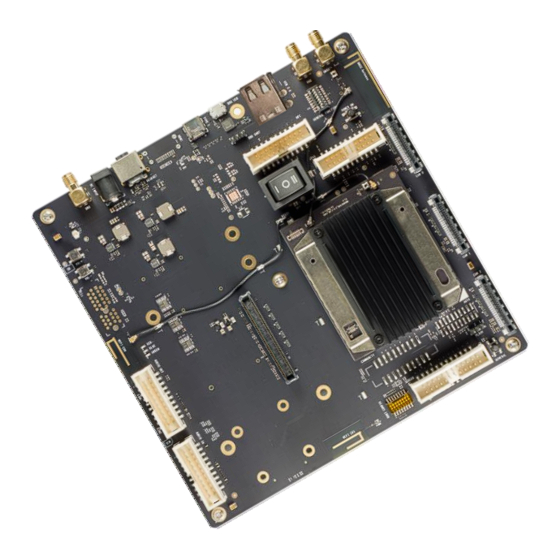
Page 13: Open-Q 660 Processor Board
• Snapdragon 660 (SDA660) main application processor • Memory (eMCP/uMCP compatible design) o Note: eMCP is the only configuration available from Intrinsyc • eMCP: 64GB eMMC 5.1 + LPDDR4x up to 1866MHz 6GB RAM • uMCP: 128GB UFS 2.1 + LPDDR4x up to 1866MHz 6GB RAM •... -
Page 14: Processor Board Mechanical Properties
3.7.2 Processor Board Block Diagram The Open-Q 660 Processor board measuring 60mm x 70mm is where all the processing occurs. It is connected to the carrier via two 240-pin high speed board-to-board connector. The purpose of the connectors is to bring out essential signals such that other peripherals can interface with the platform. - Page 15 1x4 lanes 1x4 lanes SDA660 Data/Clk UFS2.1 M-PHY EBI0 EBI1 8bit eMMC5.1 3.0GHz CLK 8.6Gbps eMCP 12x15mm QLINK QLINK 4bit SD3.0 SDC2 clk/data USB3.1+DP USB2.0 JTAG BLSP2_UART UART Figure 5 Open-Q 660 Processor Board Block Diagram Copyright Intrinsyc Technologies Corporation...
-
Page 16: Hardware Specification
2 x 240 pin B2B connector board connector 3.8 Open-Q 660 Carrier Board The Open-Q 660 Carrier board is a Mini-ITX form factor board with various connectors used for connecting different peripherals. The following are the mechanical properties of the carrier board:... -
Page 17: Dip Switch S10 Configuration Options
3.8.1 Dip switch S10 Configuration Options There is a DIP switch S2301 on the south top side of the Open-Q 660 carrier board. The 8-bit switch allows the user to control the system configuration and boot options. Table 3.8-1 below outlines the pin outs and connections of this DIP switches. - Page 18 Carrier board S2301-6 S2301-7 S2301-8 There is another DIP switch S2302 on the north top side of Open-Q 660 carrier board. The 8-bit switch allows the user to control the system configuration and boot options. Copyright Intrinsyc Technologies Corporation...
- Page 19 OFF Note: SSC SPI2 is routed to BLSP_TP by default Warning! : Before making any changes to the dip switch, make sure to note down the previous configuration. The default switch settings are above. Copyright Intrinsyc Technologies Corporation...
-
Page 20: Carrier Board Expansion Connectors
USB 2.0 Host USB 2.0 Host Type-A dual port header For Mouse and Keyboard USB 3.1 USB 3.1 Type-C header Transfer data to and from 2.4 – 5 GHz WLAN Antenna 1X PCB Antenna Antenna to Carrier board Copyright Intrinsyc Technologies Corporation... -
Page 21: Power Options
3.8.2.1 Power Options The Open-Q 660 Hardware Development Kit power source connects to the 12V DC power supply jack J0701. Starting from the power jack, the 12V power supply branches off into Copyright Intrinsyc Technologies Corporation... -
Page 22: Debug Serial Uart Header J2103
Please see the carrier board schematic for details on what to install for this header to be functional. The header consists of TX, RX and GND pins. It is a 3.3V TTL UART header. To get the serial terminal working with a PC, the following cable (or similar) is needed Copyright Intrinsyc Technologies Corporation... -
Page 23: Debug Serial Uart Over Usb J2102
This connector provides a JTAG interface to the main processor by which users can connect a JTAG (Lauterbach / USB Wiggler) 20 pin ARM JTAG. NOTE: The development kit does not include software support for JTAG Copyright Intrinsyc Technologies Corporation... -
Page 24: Sensor Io Expansion Header J2501
If user application does not require a sensor, then this header can be used for other applications that require I2C or GPIO input and output connections. Following is the pin breakout for sensor expansion header J2501 Copyright Intrinsyc Technologies Corporation... - Page 25 SSC power SSC_PWR_E J2501[24] enable In summary, if sensor application is not needed, this expansion header can provide SSC SPI1 and I2C. Please refer to the schematic and consider the power before connecting anything to this header. Copyright Intrinsyc Technologies Corporation...
-
Page 26: Nfc Expansion Header J2401
This header also allows user to connect to the free GPIOs and I2C lines when NFC is not used; therefore, enabling other use cases. Please refer to Table below for detailed information regarding the signals that are being brought out by this connector. Copyright Intrinsyc Technologies Corporation... - Page 27 J2401[20] via SDA via SDA GPIO2 GPIO0 In general, if there is no need for NFC application, this expansion header can provide two GPIOs, I2C, free running clocks, and enable voltage/ power source to external peripherals. Copyright Intrinsyc Technologies Corporation...
-
Page 28: Anc Headset Jack J1501
This header expansion provides the following audio inputs: 3 digital mics 3 analog mics Voltage rails to support analog and digital mics The table below outlines the pin out information of the audio inputs expansion header J1601: Copyright Intrinsyc Technologies Corporation... -
Page 29: Audio Outputs Expansion Header J1602
This header expansion provides the following audio outputs: 2 differential analog audio line out 2 single ended analog audio line out 1 differential analog earpiece amplifier output (no external amp needed) 2 speaker amplifier enable control Copyright Intrinsyc Technologies Corporation... - Page 30 Speaker Speaker SPKR_AMP_E WSA_EN J1602[15] J1602[16] amplifier amplifier N2(DNI) enable 1 enable 2 1.8V output VREG_S4A_1 J1602[17] 12V output DC_IN_12V J1602[18] power supply power supply 5.0V output MB_VREG_5P J1602[19] J1602[20] power supply Copyright Intrinsyc Technologies Corporation...
-
Page 31: Usb Type A Connector J1101
WiFi module on the carrier board via coaxial cables that attaches to MH4L receptacles. These antennas connect to the carrier board in the following configuration: WLAN0 on the carrier board connects to ANT0 on the WCN3980 WiFi module Copyright Intrinsyc Technologies Corporation... -
Page 32: On Board Pcb Gnss Antenna
Carrier board by default, meanwhile, there are 0ohm jumpers for user to use an external GNSS antenna via the SMA connector. The option pads are between the antenna and the eLNA input. Copyright Intrinsyc Technologies Corporation... -
Page 33: Gnss Sma Connector J3802
Uses JAE FI-RE41S-VF connector for exposing MIPI, CLK, GPIOs and Power rails. Please use JAE FI-RE41S-VF connector to access signals such as MIPI, CLK, GPIO and power rails Figure 21 Camera Connectors (J1701, J1801, J1901) Copyright Intrinsyc Technologies Corporation... - Page 34 GPIO36. Default use is for camera CCI0 (SDA_GPIO36) (SDA_GPIO36) (SDA_GPIO36) I2C data interface CAM_MCLK0_BU CAM_MCLK2_BU CAM_MCLK1_BUF Output. Connected to SDA660 GPIO32 / F (SDA_GPIO32) F (SDA_GPIO34) (SDA_GPIO33) GPIO33 / GPIO34. Default use is for camera master clock. Maximum 24MHz Copyright Intrinsyc Technologies Corporation...
- Page 35 Power output. Connected to external LDO _DVDD _DVDD DVDD regulator. Default is +1.2V. Maximum current 500mA MB_VREG_5P0 MB_VREG_5P0 MB_VREG_5P0 Power output. 5V Power supply. Maximum 700mA MB_VREG_5P0 MB_VREG_5P0 MB_VREG_5P0 Power output. 5V Power supply. Maximum 700mA Copyright Intrinsyc Technologies Corporation...
- Page 36 CSI 2 Up to 1 lane 3D 1 lane 3D use case / Dual 1 lane configuration CSI0 + CSI1 + CSI2 Up to 4 lane Three 4-lane CSI (4+4+4 or 4+4+2+1) CPHY Three 3-trio CPHY1.0 Copyright Intrinsyc Technologies Corporation...
-
Page 37: Display Card
– The development platform can support the following display combinations MIPI DSI 1 x 4lane DSI0 + 1 x 4lane DSI1 2 x 4-lane DSI DPHY 1.2 Support up to WQXGA (2560 x 1600) at 60fps Copyright Intrinsyc Technologies Corporation... -
Page 38: Display Card Connector J0501
Supports up to two touch screen controllers Supports I2C or SPI via BLSP4 and SSC_SPI_2 Can chose between I2C or SPI signals via MUX Power specifications: The display card connector supports the following power domains: Copyright Intrinsyc Technologies Corporation... -
Page 39: Connecting The Display Card To The Development Kit
LCD panel. It is important to note that connector J0501 of the display card needs to connect to J1301 of the carrier board for this configuration to work. Baseband Card (2-6-2) QCT800s DSI0 1x4lanes SDA660 DSI1 1x4lanes LPI_SPI2 Figure 23 Display Card Default Configuration Copyright Intrinsyc Technologies Corporation... -
Page 40: Display Panel
This LCD panel comes preinstalled on the HDK660 display card. Below are the Panel specifications: Resolution: 1920x1080 LCD Type: AMOLED PCAP touch panel No of Lanes: 1 x 4 lane MIPI DSI interface via Display Card. Diagonal Length: 5.7” Copyright Intrinsyc Technologies Corporation...
Need help?
Do you have a question about the Open-Q 660 and is the answer not in the manual?
Questions and answers