Table of Contents
Advertisement
Quick Links
Advertisement
Table of Contents

Subscribe to Our Youtube Channel
Related Manuals for Alinx AC7010C


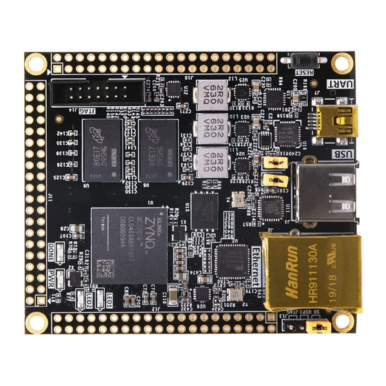
Summary of Contents for Alinx AC7010C
- Page 1 ZYNQ7000 FPGA Core Board AC7010C/AC7020C User Manual...
-
Page 2: Version Record
AC7010C / AC7020C User Manual Version Record Revision Date Release By Description Rev 1.0 2022-09-07 www.alinx.com 2 / 40... -
Page 3: Table Of Contents
AC7010C / AC7020C User Manual Table of Contents Version Record .....................2 Part 1: Introduction ..................5 Part 2: Dimensional structure ...............8 Part 3: Power Supply ..................8 Part 4: ZYNQ Chip ..................10 Part 4.1: JTAG Interface ..............13 Part 4.2: FPGA Power System ............14 Part 4.3: ZYNQ boot configuration ............. - Page 4 AC7010C / AC7020C User Manual The two core boards of the ALINX XILINX ZYNQ7000 development platform were officially released in 2022, models: AC7010C and AC7020C (industrial grade). Their development platform is the solution for XILINX's Zynq7000 SOC chip. It uses ARM+FPGA SOC technology to integrate dual-core ARM Cortex-A9 and FPGA programmable logic on a single chip.
-
Page 5: Part 1: Introduction
AC7010C/AC7020C is provided. The core board uses Xilinx's Zynq7000 series of chips, the AC7010C uses the Zynq7000's XC7Z010-1CLG400C chip, and the AC7020C uses the Zynq7000's XC7Z020-2CLG400I chip, both of which are 400-pin FBGA packages. The ZYNQ7000 chip can be divided into a processor system part processor system (PS) and a programmable logic part Programmable Logic (PL). - Page 6 AC7010C / AC7020C User Manual On the AC7010C/AC7020C core board, the PS part of the ZYNQ7000 is equipped with a wealth of external interfaces and devices for user convenience and function verification. The IO ports on the PL side are all led to the 2.54mm connector on the board for user expansion.
- Page 7 3-way 40-pin expansion port (0.1inch Spacing) 3-way 40-pin 0.1inch spacing expansion port for extending the IOs of ZYNQ PL and PL parts, and can be connect to various ALINX modules (binocular camera, TFT LCD screen, high-speed AD module, etc.) ...
-
Page 8: Part 2: Dimensional Structure
AC7010C / AC7020C User Manual Used to debug and download the ZYNQ system Micro SD card holder 1-channel Micro SD card holder, to insert SD card for stores operating system images and file systems. Part 2: Dimensional structure The size of the development board is 2.95 inch x 2.52 inch, and the PCB is designed with an 8-layer board. - Page 9 AC7010C/AC7020C core board is powered by the carrier board, remove the 0Ω resistor (R161) on the board. Please do not use other specifications of the power supply to avoid damage to the core board. The power supply design on...
-
Page 10: Part 4: Zynq Chip
Part 4: ZYNQ Chip The Core development board uses Xilinx's Zynq7000 series chip, AC7010C chip model is XC7Z010-1CLG400C (AC7020C chip model is XC7Z020-2CLG400I). The chip's PS system integrates two ARM CortexTM-A9 processors, AMBA® interconnects, internal memory, external memory www.alinx.com... - Page 11 AC7010C / AC7020C User Manual interfaces and peripherals. These peripherals mainly include USB bus interface, Ethernet interface, SD/SDIO interface, I2C bus interface, CAN bus interface, UART interface, GPIO etc. The PS can operate independently and start up at power up or reset. Figure 4-1 detailed the Overall Block Diagram of the ZYNQ7000 Chip.
- Page 12 E3, G3, etc., Therefore, when we look at the schematic, we see the form of the letter + number, which represents the pin of the BGA. Figure 4-2 detailed the XC7Z010 chip on the Core Board AC7010C. www.alinx.com 12 / 40...
-
Page 13: Part 4.1: Jtag Interface
AC7010C / AC7020C User Manual Figure 4-2: The XC7Z010 chip on the Core Board AC7010C Part 4.1: JTAG Interface First, let's talk about the JTAG debug interface (J14) of the AC7010C/AC7020C core board. Users can debug and download the ZYNQ program by connecting the ALINX Xilinx USB Cable downloader. -
Page 14: Part 4.2: Fpga Power System
VCCAUX is the FPGA auxiliary power supply pin, connected to 1.8V; VCCO is the voltage of each BANK of PL, including BANK13, BANK34, BANK35, on the AC7010C/AC7020C FPGA Core board, the voltage of BANK is connected to 3.3V. The voltage of BANK34 and BANK35 can be adjusted by replacing the LDO chip. -
Page 15: Part 4.3: Zynq Boot Configuration
Table 4-1: J13 startup mode configuration Part 5: Clock Configuration The AC7010C/AC7020C core board provides an active clock for the PS system, and the clock of the PL logic part can be generated by the PLL of the PS part. Alternatively, the 50Mhz crystal oscillator can be used to provide a clock source to achieve separate operation of the PS system and PL logic. -
Page 16: Part 5.2: Pl System Clock Source
PS_CLK_500 Part 5.2: PL system clock source The AC7010C/AC7020C FPGA core board, The PL system clock on the AC7010C/AC7020C core board is powered by a 50MHz active crystal. This 50Mhz clock can be used to drive user logic in the FPGA. The schematic diagram of the clock source is shown in Figure 5-3. -
Page 17: Part 6.1: Qspi Flash
PS part. Part 6.1: QSPI Flash The AC7010C/AC7020C FPGA core board is equipped with a 256MBit Quad-SPI FLASH chip, model W25Q256, which uses the 3.3V CMOS voltage standard. Due to the non-volatile nature of QSPI FLASH, it can be used as a boot device for the system to store the boot image of the system. -
Page 18: Part 6.2: Ddr3 Dram
Configure chip pin assignments: Signal Name ZYNQ Pin Name ZYNQ Pin Number QSPI_SCK PS_MIO6_500 QSPI_CS PS_MIO1_500 QSPI_D0 PS_MIO2_500 QSPI_D1 PS_MIO3_500 QSPI_D2 PS_MIO4_500 QSPI_D3 PS_MIO5_500 Part 6.2: DDR3 DRAM The AC7010C FPGA core board is equipped with two SKHynix 2Gbit www.alinx.com 18 / 40... - Page 19 AC7010C / AC7020C User Manual DDR3 chips (total 4Gbit), model H5TQ2G63FFR-RDC (compatible with MT41J128M16HA-125). The AC7020C FPGA core board is equipped with two SKHynix 4Gbit DDR3 chips (total 8Gbit), model H5TQ4G63AFR-PBI (compatible with MT41J256M16RE-125). The bus width of DDR is 32bits in total, and the maximum operating speed of DDR3 SDRAM is 533MHz (data rate 1066Mbps).
- Page 20 AC7010C / AC7020C User Manual Figure 6-2: The Schematic Part of DDR3 DRAM Figure 6-3: Two DDR3 DRAMs on the FPGA Core Board www.alinx.com 20 / 40...
- Page 21 AC7010C / AC7020C User Manual DDR3 Pin Assignment: Signal Name ZYNQ Pin Name ZYNQ Pin Number DDR3_DQS0_P PS_DDR_DQS_P0_502 DDR3_DQS0_N PS_DDR_DQS_N0_502 DDR3_DQS1_P PS_DDR_DQS_P1_502 DDR3_DQS1_N PS_DDR_DQS_N1_502 DDR3_DQS2_P PS_DDR_DQS_P2_502 DDR3_DQS2_N PS_DDR_DQS_N2_502 DDR3_DQS3_P PS_DDR_DQS_P3_502 DDR3_DQS4_N PS_DDR_DQS_N3_502 DDR3_DQ[0] PS_DDR_DQ0_502 DDR3_DQ [1] PS_DDR_DQ1_502 DDR3_DQ [2] PS_DDR_DQ2_502...
- Page 22 AC7010C / AC7020C User Manual DDR3_DQ [26] PS_DDR_DQ26_502 DDR3_DQ [27] PS_DDR_DQ27_502 DDR3_DQ [28] PS_DDR_DQ28_502 DDR3_DQ [29] PS_DDR_DQ29_502 DDR3_DQ [30] PS_DDR_DQ30_502 DDR3_DQ [31] PS_DDR_DQ31_502 DDR3_DM0 PS_DDR_DM0_502 DDR3_DM1 PS_DDR_DM1_502 DDR3_DM2 PS_DDR_DM2_502 DDR3_DM3 PS_DDR_DM3_502 DDR3_A[0] PS_DDR_A0_502 DDR3_A[1] PS_DDR_A1_502 DDR3_A[2] PS_DDR_A2_502 DDR3_A[3] PS_DDR_A3_502 DDR3_A[4]...
-
Page 23: Part 6.3: Gigabit Ethernet Interface
AC7010C / AC7020C User Manual DDR3_CKE PS_DDR_CKE_502 Part 6.3: Gigabit Ethernet Interface AC7010C/AC7020C FPGA core board provides network communication services to users through JLSemi JL2121-N040I Ethernet GPHY chip. he Ethernet PHY chip on the PS side is connected to the GPIO interface of the BANK501 of the PS side of ZYNQ. - Page 24 AC7010C / AC7020C User Manual the transmission clock is 25Mhz. Data is sampled on the rising edge and falling samples of the clock. Figure 6-4: The connection of the ZYNQ and GPHY chip The Gigabit Ethernet pin assignments are as follows:...
-
Page 25: Part 6.4: Usb2.0 Interface
AC7010C / AC7020C User Manual Part 6.4: USB2.0 Interface The USB2.0 transceiver used in the AC7010C/AC7020C is a 1.8V, high-speed USB3320C-EZK that supports the ULPI standard interface. ZYNQ's USB bus interface is connected to the USB3320C-EZK transceiver for high-speed USB2.0 Host mode and Slave mode data communication. The USB3320C's USB data and control signals are connected to the IO port of the BANK501 on the PS side of the ZYNQ chip. - Page 26 AC7010C / AC7020C User Manual Figure 6-6: The connection between Zynq7000 and USB chip Figure 6-7 shows the physical diagram of the USB2.0 part. U11 is USB3320C, J3 is the Host USB interface, and J4 is the OTG USB interface.
-
Page 27: Part 6.5: Usb To Serial Port
AC7010C / AC7020C User Manual Part 6.5: USB to Serial Port The AC7100/AC7200 FPGA development board uses the USB to UART chip of Silicon Labs CP2102GM. The USB interface uses the Micro USB interface. Users can connect to the PC for serial communication using a Micro USB cable. -
Page 28: Part 6.6: Sd Card Slot
AC7010C/AC7020C FPGA core board. Part 6.6: SD Card Slot The AC7010C/AC7020C core board contains a Micro SD card interface to provide user access to the SD card memory, the BOOT program for storing the ZYNQ chip, the Linux operating system kernel, the file system and other user data files. -
Page 29: Part 6.7: User Leds
SD Card Insertion Signal Part 6.7: User LEDs On the AC7010C/AC7020C core board, one LED light-emitting diode is connected to the BANK500 IO of the PS part, and the user can use this LED light to debug the program. When the BANK500 IO voltage is high, the LED light is off, and when the BANK500 IO voltage is low, the LED will be illuminated. -
Page 30: Part 6.8: Reset Key
PS User LED LED1 Part 6.8: Reset Key On the AC7010C/AC7020C core board, the entire ZYNQ system is reset by a RESET key, and the reset signal is connected to the PS pin's reset pin PS_POR_B_500. The user can use this user key to manually reset. In the design, when the reset key is pressed, the reset signal is low, and the ZYNQ chip is reset. -
Page 31: Part 7:Zynq Pl Peripherals
Part 7:ZYNQ PL Peripherals Part 7.1: User LEDs The PL part of the AC7010C/AC7020C FPGA core board is also connected to one LED light-emitting diode. The schematic diagram is shown in Figure 7-1, The LED signal is connected to the IO of the PL part BANK34. -
Page 32: Part 7.2: Expansion Port J10
AC7010C / AC7020C User Manual Figure 7-2: PL User LEDs on the FPGA Core Board PL User LEDs pin assignment: Signal Name ZYNQ Pin Name ZYNQ Pin Number Description LED2 IO_0_34 PL User LED PL LED2 Part 7.2: Expansion Port J10 The expansion port J10 is a 40-pin 2.54mm double-row connector, which... - Page 33 AC7010C / AC7020C User Manual Figure 7-3: Expansion header J10 schematic Figure 7-4: Expansion header J10 on the FPGA Board J10 Expansion Header Pin Assignment J10 Pin Signal Name ZYNQ Pin Number PIN1 PIN2 PIN3 IO34_L14N PIN4 IO34_L14P PIN5 IO34_L9N...
-
Page 34: Part 7.3: Expansion Port J11
The expansion port J11, which expands more peripherals and interfaces for users. Currently, the J11 interface can be directly connected to the module provided by ALINX, include: ADDA module, LCD module, Gigabit Ethernet module, audio input/output module, matrix keyboard module, 500W binocular vision camera module, etc. - Page 35 AC7010C / AC7020C User Manual The expansion port has 40 signals, of which 1-channel 5V power supply, 2-channel 3.3 V power supply, 3-channle ground and 34 IOs. 34 IO ports are connected to BANK34 and BANK35 of ZYNQ PL. The PCB design is differentially connected.
- Page 36 AC7010C / AC7020C User Manual Figure 7-5: Expansion Port J11 schematic Figure 7-6: Expansion header J11 on the FPGA Board J11 Expansion Header Pin Assignment J11 Pin Signal Name ZYNQ Pin Number PIN1 PIN2 PIN3 IO34_L23P PIN4 IO34_L23N PIN5 IO34_L24P...
-
Page 37: Part 7.4: Expansion Port J12
AC7010C / AC7020C User Manual PIN14 IO34_L15P PIN15 IO34_L24P PIN16 IO34_24N PIN17 IO34_L11P PIN18 IO34_L11N PIN19 IO34_L19P PIN20 IO34_L19N PIN21 IO34_L16N PIN22 IO34_L16P PIN23 IO34_L22N PIN24 IO34_L22P PIN25 IO34_L17P PIN26 IO34_L17N PIN27 IO34_L21P PIN28 IO34_L21N PIN29 IO34_L18P PIN30 IO34_L18N PIN31... - Page 38 AC7010C / AC7020C User Manual interfaces for users. Currently, the J12 interface can be directly connected to the module provided by ALINX, include: ADDA module, LCD module, Gigabit Ethernet module, audio input/output module, matrix keyboard module, 500W binocular vision camera module, etc.
- Page 39 AC7010C / AC7020C User Manual J12 Expansion Header Pin Assignment J11 Pin Signal Name ZYNQ Pin Number PIN1 PIN2 PIN3 IO35_L3N PIN4 IO35_L3P PIN5 IO35_L6P PIN6 IO35_L6N PIN7 IO35_L18P PIN8 IO35_L18N PIN9 IO35_L14P PIN10 IO35_L14N PIN11 IO35_L17N PIN12 IO35_L17P PIN13...
- Page 40 AC7010C / AC7020C User Manual PIN35 PS_MIO10 PIN36 PS_MIO12 PIN37 PIN38 PIN39 +3.3V PIN40 +3.3V www.alinx.com 40 / 40...
Need help?
Do you have a question about the AC7010C and is the answer not in the manual?
Questions and answers