Table of Contents
Advertisement
Quick Links
Advertisement
Table of Contents

Related Manuals for Alinx AC7200


Summary of Contents for Alinx AC7200
- Page 1 ARTIX-7 FPGA Development Board AC7200 System on Module...
-
Page 2: Version Record
First Release The English version of the user manual was translated by Shanghai Tianhui Trading Company. It has not been officially Review by ALINX and is for reference only. If there are any errors, please send email feedback to rachel.zhou@aithtech.com for correction. -
Page 3: Table Of Contents
ARTIX-7 SoM FPGA Core Board AC7200 User Manual Table of Contents Version Record .....................2 Part 1: AC7200 Core Board Introduction .............4 Part 2: FPGA Chip ..................6 Part 3: Active Differential Crystal ..............8 Part 3.1: 200Mhz Active Differential clock ..........8 Part 3.2: 125Mhz differential clock ............ -
Page 4: Part 1: Ac7200 Core Board Introduction
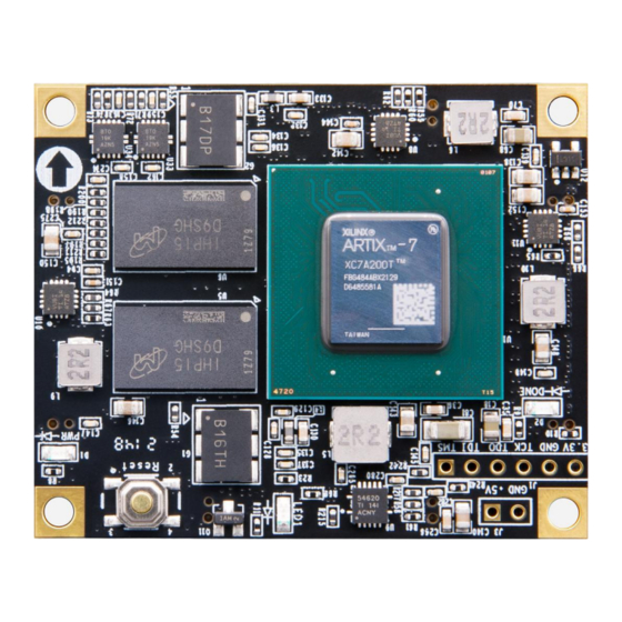
ARTIX-7 SoM FPGA Core Board AC7200 User Manual Part 1: AC7200 Core Board Introduction AC7200 (core board model, the same below) FPGA core board, it is based XILINX's ARTIX-7 series 200T XC7A200T-2FGG484I. high-performance core board with high speed, high bandwidth and high capacity. - Page 5 ARTIX-7 SoM FPGA Core Board AC7200 User Manual Figure 1-1: AC7200 Core Board (Front View) Figure 1-2: AC7200 Core Board (Rear View) Amazon Store: https://www.amazon.com/alinx 5 / 30 Sales Email: rachel.zhou@aithtech.com...
-
Page 6: Part 2: Fpga Chip
ARTIX-7 SoM FPGA Core Board AC7200 User Manual Part 2: FPGA Chip As mentioned above, the FPGA model we use is XC7A200T-2FGG484I, which belongs to Xilinx's Artix-7 series. The speed grade is 2, and the temperature grade is industry grade. This model is a FGG484 package with 484 pins. - Page 7 CCAUX each BANK of FPGA, including BANK0, BANK13~16, BANK34~35. On AC7200 FPGA core board, BANK34 and BANK35 need to be connected to DDR3, the voltage connection of BANK is 1.5V, and the voltage of other BANK is 3.3V. The VCCO of BANK15 and BANK16 is powered by the LDO, and can be changed by replacing the LDO chip.
-
Page 8: Part 3: Active Differential Crystal
ARTIX-7 SoM FPGA Core Board AC7200 User Manual Part 3: Active Differential Crystal The AC7200 core board is equipped with two Sitime active differential crystals, one is 200MHz, the model is SiT9102-200.00MHz, the system main clock for FPGA and used to generate DDR3 control clock; the other is 125MHz, model is SiT9102 -125MHz, reference clock input for GTP transceivers. -
Page 9: Part 3.2: 125Mhz Differential Clock
ARTIX-7 SoM FPGA Core Board AC7200 User Manual Figure 3-2: 200Mhz Active Differential Crystal on the Core Board 200Mhz Differential Clock Pin Assignment Signal Name FPGA PIN SYS_CLK_P SYS_CLK_N Part 3.2: 125Mhz differential clock G2 in Figure 3.3 is the 125M active differential crystal oscillator circuit. This clock is the reference input clock provided to the GTP module inside the FPGA. - Page 10 ARTIX-7 SoM FPGA Core Board AC7200 User Manual Figure 3-4: 125Mhz Active Differential Crystal on the Core Board 125Mhz Differential Clock Pin Assignment Net Name FPGA PIN MGT_CLK0_P MGT_CLK0_N Amazon Store: https://www.amazon.com/alinx 10 / 30 Sales Email: rachel.zhou@aithtech.com...
-
Page 11: Part 4: Ddr3 Dram
ARTIX-7 SoM FPGA Core Board AC7200 User Manual Part 4: DDR3 DRAM The FPGA core board AC7200 is equipped with two Micron 4Gbit (512MB) DDR3 chips, model MT41J256M16HA-125 (compatible with MT41K256M16HA-125). The DDR3 SDRAM has a maximum operating speed of 800MHz (data rate 1600Mbps). The DDR3 memory system is directly connected to the memory interface of the BANK 34 and BANK35 of the FPGA. - Page 12 ARTIX-7 SoM FPGA Core Board AC7200 User Manual Figure 4-2: The DDR3 on the Core Board DDR3 DRAM pin assignment: Signal Name FPGA Pin Name FPGA Pin Number DDR3_DQS0_P IO_L3P_T0_DQS_AD5P_35 DDR3_DQS0_N IO_L3N_T0_DQS_AD5N_35 DDR3_DQS1_P IO_L9P_T1_DQS_AD7P_35 DDR3_DQS1_N IO_L9N_T1_DQS_AD7N_35 DDR3_DQS2_P IO_L15P_T2_DQS_35 DDR3_DQS2_N IO_L15N_T2_DQS_35...
- Page 13 ARTIX-7 SoM FPGA Core Board AC7200 User Manual DDR3_DQ [10] IO_L8P_T1_AD14P_35 DDR3_DQ [11] IO_L10N_T1_AD15N_35 DDR3_DQ [12] IO_L7N_T1_AD6N_35 DDR3_DQ [13] IO_L10P_T1_AD15P_35 DDR3_DQ [14] IO_L7P_T1_AD6P_35 DDR3_DQ [15] IO_L12P_T1_MRCC_35 DDR3_DQ [16] IO_L18N_T2_35 DDR3_DQ [17] IO_L16P_T2_35 DDR3_DQ [18] IO_L14P_T2_SRCC_35 DDR3_DQ [19] IO_L17N_T2_35 DDR3_DQ [20]...
- Page 14 ARTIX-7 SoM FPGA Core Board AC7200 User Manual DDR3_A[10] IO_L5N_T0_34 DDR3_A[11] IO_L4P_T0_34 DDR3_A[12] IO_L4N_T0_34 DDR3_A[13] IO_L1N_T0_34 DDR3_A[14] IO_L6N_T0_VREF_34 DDR3_BA[0] IO_L9N_T1_DQS_34 DDR3_BA[1] IO_L9P_T1_DQS_34 DDR3_BA[2] IO_L11P_T1_SRCC_34 DDR3_S0 IO_L8P_T1_34 DDR3_RAS IO_L12P_T1_MRCC_34 DDR3_CAS IO_L12N_T1_MRCC_34 DDR3_WE IO_L7P_T1_34 DDR3_ODT IO_L14N_T2_SRCC_34 DDR3_RESET IO_L15P_T2_DQS_34 DDR3_CLK_P IO_L3P_T0_DQS_34 DDR3_CLK_N IO_L3N_T0_DQS_34...
-
Page 15: Part 5: Qspi Flash
ARTIX-7 SoM FPGA Core Board AC7200 User Manual Part 5: QSPI Flash The FPGA core board AC7200 is equipped with one 128MBit QSPI FLASH, and the model is N25Q128, which uses the 3.3V CMOS voltage standard. Due to the non-volatile nature of QSPI FLASH, it can be used as a boot device for the system to store the boot image of the system. - Page 16 ARTIX-7 SoM FPGA Core Board AC7200 User Manual QSPI Flash pin assignments: Signal Name FPGA Pin Name FPGA Pin Number QSPI_CLK CCLK_0 QSPI_CS IO_L6P_T0_FCS_B_14 QSPI_DQ0 IO_L1P_T0_D00_MOSI_14 QSPI_DQ1 IO_L1N_T0_D01_DIN_14 QSPI_DQ2 IO_L2P_T0_D02_14 QSPI_DQ3 IO_L2N_T0_D03_14 Figure 5-2: QSPI on the Core Board Amazon Store: https://www.amazon.com/alinx...
-
Page 17: Part 6: Led Light On Core Board
ARTIX-7 SoM FPGA Core Board AC7200 User Manual Part 6: LED Light on Core Board There are 3 red LED lights on the AC7200 FPGA core board, one of which is the power indicator light (PWR), one is the configuration LED light (DONE), and one is the user LED light. -
Page 18: Part 7: Reset Key
ARTIX-7 SoM FPGA Core Board AC7200 User Manual Part 7: Reset Key There is a reset key on the AC7200 FPGA core board. The reset key is connected to the normal IO of the BANK34 of the FPGA chip. The user can use this reset key to initialize the FPGA program. -
Page 19: Part 8: Jtag Interface
ARTIX-7 SoM FPGA Core Board AC7200 User Manual Part 8: JTAG Interface The JTAG test socket J1 is reserved on the AC7200 core board for JTAG download and debugging when the core board is used alone. Figure 8-1 is the schematic part of the JTAG port, which involves TMS, TDI, TDO, TCK. -
Page 20: Part 9: Power Interface On The Core Board
ARTIX-7 SoM FPGA Core Board AC7200 User Manual Part 9: Power Interface on the Core Board In order to make the AC7200 FPGA core board work alone, the core board is reserved with the 2PIN power interface (J3). When the user supplies power to the core board through 2PIN power interface (J3), it cannot be powered through the carrier board. -
Page 21: Part 10: Board To Board Connectors
ARTIX-7 SoM FPGA Core Board AC7200 User Manual Part 10: Board to Board Connectors The core board has a total of four high-speed board to board connectors. The core board uses four 80-pin inter-board connectors to connect to the carrier board. The IO port of the FPGA is connected to the four connectors by differential routing. - Page 22 ARTIX-7 SoM FPGA Core Board AC7200 User Manual PIN11 PIN12 PIN13 PIN14 PIN15 PIN16 B13_L4_P AA15 3.3V PIN17 PIN18 B13_L4_N AB15 3.3V PIN19 Ground PIN20 Ground PIN21 B13_L5_P 3.3V PIN22 B13_L1_P 3.3V PIN23 B13_L5_N AA14 3.3V PIN24 B13_L1_N AA16 3.3V...
- Page 23 ARTIX-7 SoM FPGA Core Board AC7200 User Manual Board to Board Connectors CON2 The 80-pin female connection header CON2 is used to extend the normal IO of the BANK13 and BANK14 of the FPGA. The voltage standards of both BANKs are 3.3V.
- Page 24 ARTIX-7 SoM FPGA Core Board AC7200 User Manual PIN55 B14_L18_N 3.3V PIN56 B14_L13_N 3.3V PIN57 B14_L18_P 3.3V PIN58 B14_L13_P 3.3V PIN59 Ground PIN60 Ground PIN61 B13_L17_P 3.3V PIN62 B14_L3_N 3.3V PIN63 B13_L17_N 3.3V PIN64 B14_L3_P 3.3V PIN65 B14_L21_N 3.3V PIN66 B14_L20_N 3.3V...
- Page 25 ARTIX-7 SoM FPGA Core Board AC7200 User Manual PIN19 Ground PIN20 Ground PIN21 B15_L11_P 3.3V PIN22 B16_L24_P 3.3V PIN23 B15_L11_N 3.3V PIN24 B16_L24_N 3.3V PIN25 B15_L1_N 3.3V PIN26 B15_L8_N 3.3V PIN27 B15_L1_P 3.3V PIN28 B15_L8_P 3.3V PIN29 Ground PIN30 Ground...
- Page 26 ARTIX-7 SoM FPGA Core Board AC7200 User Manual of the IO port of BANK16 can be adjusted by an LDO chip. The default installed LDO is 3.3V. If the user wants to output other standard levels, it can be replaced by a suitable LDO. The high-speed data and clock signals of the GTP are strictly differential routed on the core board.
- Page 27 ARTIX-7 SoM FPGA Core Board AC7200 User Manual PIN49 Ground PIN50 Ground PIN51 B16_L9_P 3.3V PIN52 B16_L10_P 3.3V PIN53 B16_L9_N 3.3V PIN54 B16_L10_N 3.3V PIN55 B16_L11_P 3.3V PIN56 B16_L12_P 3.3V PIN57 B16_L11_N 3.3V PIN58 B16_L12_N 3.3V PIN59 Ground PIN60 Ground...
-
Page 28: Part 11: Power Supply
ARTIX-7 SoM FPGA Core Board AC7200 User Manual Part 11: Power Supply The AC7200 FPGA core board is powered by DC5V via carrier board, and it is powered by the J3 interface when it is used alone. Please be careful not to supply power by the J3 interface and the carrier board at the same time to avoid damage. - Page 29 ARTIX-7 SoM FPGA Core Board AC7200 User Manual generated by one LDOSPX3819M5-3-3. VCCIO mainly supplies power to BANK15 and BANK16 of FPGA. Users can change the IO of BANK15,16 to different voltage standards by replacing their LDO chip. 1.5V Generates the VTT and VREF voltages required by DDR3 via TI's TPS51200.
-
Page 30: Part 12: Form Factors
ARTIX-7 SoM FPGA Core Board AC7200 User Manual Part 12: Form Factors Figure 12-1: AC7200 FPGA Core board (Top view) Figure 12-2: AC7200 FPGA Core board (Bottom view) Amazon Store: https://www.amazon.com/alinx 30 / 30 Sales Email: rachel.zhou@aithtech.com...
Need help?
Do you have a question about the AC7200 and is the answer not in the manual?
Questions and answers