Table of Contents
Advertisement
Quick Links
Advertisement
Table of Contents

Related Manuals for Alinx AC7015


Summary of Contents for Alinx AC7015
- Page 1 ZYNQ7000 FPGA Development Board AC7015 System on Module...
-
Page 2: Version Record
2020-06-29 Rachel Zhou First Release The English version as translated by Shanghai Tianhui Trading Company. It has not been officially Review by ALINX and is for reference only. If there are any errors, please send email feedback to rachel.zhou@aithtech.com correction. -
Page 3: Table Of Contents
ZYNQ FPGA Development Platform AC7015 User Manual Tabel of Contents Version Record ......................2 Part 1: AC7015 Core Board Introduction ..............4 Part 2: ZYNQ Chip ...................... 6 Part 3: DDR3 DRAM ....................8 Part 4: QSPI Flash ....................11 Part 5: eMMC Flash ....................12 Part 6: Clock configuration .................. -
Page 4: Part 1: Ac7015 Core Board Introduction
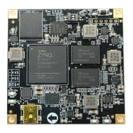
ZYNQ FPGA Development Platform AC7015 User Manual Part 1: AC7015 Core Board Introduction The AC7015 (core board model, the same below) core board is an FPGA development board based on the Zynq chip XC7Z015-2CLG485I of the XILINX ZYNQ7000 series. The ZYNQ chip's PS system integrates two ARM CortexTM-A9 processors, AMBA®... - Page 5 ZYNQ FPGA Development Platform AC7015 User Manual Figure 1-1: AC7015 Core board Front View Figure 1-2: AC7015 Core Board Rear View Amazon Store: https://www.amazon.com/alinx 5 / 31 Sales Email: rachel.zhou@aithtech.com...
-
Page 6: Part 2: Zynq Chip
ZYNQ FPGA Development Platform AC7015 User Manual Part 2: ZYNQ Chip The development board uses Xilinx's Zynq7000 series chip, model XC7Z015- 2CLG485I. The chip's PS system integrates two ARM CortexTM-A9 processors, AMBA® interconnects, internal memory, external memory interfaces and peripherals. These peripherals mainly include USB bus interface, Ethernet interface, SD/SDIO interface, I2C bus interface, CAN bus interface, UART interface, GPIO etc. - Page 7 ZYNQ FPGA Development Platform AC7015 User Manual interface Two Gigabit NIC support: divergent-aggregate DMA, GMII, RGMII, SGMII interface Two USB2.0 OTG interfaces, each supporting up to 12 nodes Two CAN2.0B bus interfaces Two SD card, SDIO, MMC compatible controllers ...
-
Page 8: Part 3: Ddr3 Dram
Figure 2-3: TheXC7Z020 chip used on the Core Board Part 3: DDR3 DRAM The AC7015 core board is equipped with two SK Hynix DDR3 SDRAM chips (1GB total), model H5TQ4G63AFR-PBI. The bus width of DDR3 SDRAM is 32 bits in total. DDR3 SDRAM has a maximum operating speed of 533MHz (data rate 1066Mbps). - Page 9 ZYNQ FPGA Development Platform AC7015 User Manual Figure 3-1: The Schematic part of DDR3 DRAM Figure 3-2: DDR3 DRAM on the Core Board DDR3 DRAM Pin Assignment Signal Name ZYNQ Pin Name Pin Number DDR3_DQS0_P PS_DDR_DQS_P0_502 DDR3_DQS0_N PS_DDR_DQS_N0_502 DDR3_DQS1_P PS_DDR_DQS_P1_502...
- Page 10 ZYNQ FPGA Development Platform AC7015 User Manual DDR3_DQS3_P PS_DDR_DQS_P3_502 DDR3_DQS4_N PS_DDR_DQS_N3_502 DDR3_D0 PS_DDR_DQ0_502 DDR3_D1 PS_DDR_DQ1_502 DDR3_D2 PS_DDR_DQ2_502 DDR3_D3 PS_DDR_DQ3_502 DDR3_D4 PS_DDR_DQ4_502 DDR3_D5 PS_DDR_DQ5_502 DDR3_D6 PS_DDR_DQ6_502 DDR3_D7 PS_DDR_DQ7_502 DDR3_D8 PS_DDR_DQ8_502 DDR3_D9 PS_DDR_DQ9_502 DDR3_D10 PS_DDR_DQ10_502 DDR3_D11 PS_DDR_DQ11_502 DDR3_D12 PS_DDR_DQ12_502 DDR3_D13 PS_DDR_DQ13_502 DDR3_D14...
-
Page 11: Part 4: Qspi Flash
ZYNQ FPGA Development Platform AC7015 User Manual DDR3_BA0 PS_DDR_BA0_502 DDR3_BA1 PS_DDR_BA1_502 DDR3_BA2 PS_DDR_BA2_502 DDR3_S0 PS_DDR_CS_B_502 DDR3_RAS PS_DDR_RAS_B_502 DDR3_CAS PS_DDR_CAS_B_502 DDR3_WE PS_DDR_WE_B_502 DDR3_ODT PS_DDR_ODT_502 DDR3_RESET PS_DDR_DRST_B_502 DDR3_CLK0_P PS_DDR_CKP_502 DDR3_CLK0_N PS_DDR_CKN_502 DDR3_CKE PS_DDR_CKE_502 Table 3-2: DDR3 DRAM Pin Assignment Part 4: QSPI Flash The core board is equipped with a 256MBit Quad-SPI FLASH chip, model W25Q256FVEI, which uses the 3.3V CMOS voltage standard. -
Page 12: Part 5: Emmc Flash
ZYNQ FPGA Development Platform AC7015 User Manual Figure 4-1: QSPI Flash in the schematic Figure 4-2: QSPI Flash on the Core Board Pin Assignment of QSPI Flash Signal Name ZYNQ Pin Name Pin Number QSPI_SCK PS_MIO6_500 QSPI_CS PS_MIO1_500 QSPI_D0 PS_MIO2_500... - Page 13 ZYNQ FPGA Development Platform AC7015 User Manual model THGBMFG6C1LBAIL, which supports the JEDEC e-MMC V5.0 standard HS-MMC interface with level support of 1.8V or 3.3V. The data width of the eMMC FLASH and ZYNQ connections is 4 bits. Due to the large capacity and non-volatile...
-
Page 14: Part 6: Clock Configuration
Table 5-2: Pin Assignment of eMMC FLASH Part 6: Clock configuration AC7015 core board provides active clock for PS system, PL logic part and GTP transceiver respectively, so that PS system, PL logic and GTP transceiver can work independently. The PS and PL terminals use a single-ended crystal, and the GTP terminal uses a differential crystal. - Page 15 Table 6-1: PS Clock pin assignment PL system clock source The AC7015 core board provides a single-ended 125MHz PL system clock source with 3.3V power supply. The crystal output is connected to the global clock (MRCC) of the FPGA BANK13, which can be used to drive user logic within the FPGA.
- Page 16 Table 6-2: PL Clock pin assignment GTP differential clock The AC7015 core board provides a differential 125MHz GTP reference clock. The differential LVDS clock output is connected to the reference clock of BANK112. This 125Mhz clock can be used as the reference clock for fiber optic data communication on the carrier board.
-
Page 17: Part 7: Usb To Serial Port
MGT_CLK1_N Part 7: USB to Serial Port For the AC7015 core board to work and debug separately, we have a Uart to USB interface for the core board. Used for separate power supply and debugging of the core board. The conversion chip uses the USB-UART chip of Silicon Labs Amazon Store: https://www.amazon.com/alinx... -
Page 18: Part 8: Led Light
Table 7-1: Uart Pin Assignment Part 8: LED Light There are 4 red LED lights on the AC7015 core board, one of which is the power indicator light (PWR), one is the configuration LED light (DONE), two are the user LED lights (LED1~LED2). When the core board is powered, the power indicator will illuminate;... - Page 19 ZYNQ FPGA Development Platform AC7015 User Manual illuminate. Two user LED lights are connected to the MIO of the PS, one is connected to the IO of the PL, the user can control the lighting and off by the program, when the IO voltage connected to the user LED light is high, the user LED light is off, when the connection IO voltage is low, the user LED will be illuminated.
-
Page 20: Part 9: Reset Button
Table 8-1: LED Pin Assignment Part 9: Reset Button The AC7015 has a reset button RESET and circuitry on the core board. The reset signal is connected to the PS reset pin of the ZYNQ chip. The reset button can be used by the user to reset the ZYNQ system. When the reset button is pressed, the reset chip will generate a low level reset signal to the ZYNQ chip. -
Page 21: Part 10: Jtag Interface
ZYNQ FPGA Development Platform AC7015 User Manual Part 10: JTAG Interface The JTAG test socket J1 is reserved on the AC7015 core board for separate JTAG download and debugging of the core board. Figure 2-10-1 is the schematic part of the JTAG port, which involves TMS, TDI, TDO, TCK, GND. , +3.3V these six signals. -
Page 22: Part 11: Dip Switch Configuration
ZYNQ FPGA Development Platform AC7015 User Manual Part 11: DIP switch configuration The AC7015 has a 2-digit DIP switch SW1 on the core board to configure the ZYNQ system's startup mode. The AC7015 system development platform supports three startup modes. The three startup modes are JTAG debug mode, QSPI FLASH and SD card boot mode. - Page 23 ZYNQ FPGA Development Platform AC7015 User Manual Figure 12-1: The Power Supply Design on the Core Board The development board is powered by +5V, and is converted into +1.0V, +1.8V, +1.5V, +3.3V four-way power supply through four-way DC/DC power supply core TPS54620TLV62130RGT.
- Page 24 ZYNQ FPGA Development Platform AC7015 User Manual Clock Crystal +1.5V DDR3, ZYNQ Bank501 DDR3 VREF,VTT(+0.75V) VCCIO(+2.5V) Reserved for ZYNQ Bank33,Bank 34 Table 12-1: The Functions of Each Power Distribution Because the power supply of ZYNQ FPGA has the power-on sequence requirement, in the circuit design, we have designed according to the power requirements of the chip, and the power-on is +1.0V->+1.8V->(+1.5 V, +3.3V,...
-
Page 25: Part 13: Structure Diagram
ZYNQ FPGA Development Platform AC7015 User Manual Part 13: Structure diagram Figure 13-1: The Structure diagram (Top View) Part 14: Connector pin definition The core board expands four high-speed expansion ports, and uses four 80- pin inter-board connectors (CON1~CON4) to connect with the expansion board. - Page 26 ZYNQ FPGA Development Platform AC7015 User Manual ZYNQ Pin ZYNQ Pin CON1 Pin Signal Name CON1 Pin Signal Name Name Name PS_MIO13 ETH_TXD0 PS_MIO12 ETH_TXD1 ETH_TXD2 ETH_TXD3 ETH_TXCK ETH_TXCTL ETH_RXD3 ETH_RXD2 PS_MIO7 ETH_RXD1 PS_MIO8 ETH_RXD0 PS_MIO9 ETH_RXCTL PS_MIO11 ETH_RXCK ETH_MDC...
- Page 27 ZYNQ FPGA Development Platform AC7015 User Manual PS_MIO10 OTG_DATA1 SD_CLK OTG_DATA2 SD_D1 OTG_DATA3 SD_D0 OTG_DATA4 SD_CMD OTG_DATA5 SD_D3 OTG_DATA6 SD_D2 OTG_DATA7 FPGA_TMS FPGA_TCK FPGA_TDO FPGA_TDI Table 2-14-1: Pin Assignment of CON1 ZYNQ Pin ZYNQ Pin CON2 Pin Signal Name CON2 Pin...
- Page 28 ZYNQ FPGA Development Platform AC7015 User Manual B35_IO0 B35_L21_N B35_L20_P B35_L2_P B35_L20_N B35_L2_N B35_L5_P B35_L23_P B35_L5_N B35_L23_N B35_L6_P B35_L17_P B35_L6_N B35_L17_N B35_L1_N B35_L16_P B35_L1_P B35_L16_N B35_L14_P B35_L18_N B35_L14_N B35_L18_P B35_L12_N B35_L15_N B35_L12_P B35_L15_P B35_L11_N B35_L13_N B35_L11_P B35_L13_P B35_L3_P B35_L10_N B35_L3_N...
- Page 29 ZYNQ FPGA Development Platform AC7015 User Manual MGT_RX1_P MGT_RX1_N MGT_TX2_P MGT_TX2_N MGT_TX1_P MGT_TX1_N MGT_RX3_N MGT_RX3_P MGT_RX0_P MGT_RX0_N MGT_TX3_P MGT_TX3_N MGT_TX0_P MGT_TX0_N B34_L3_P B34_L3_N B34_L4_N B34_L4_P B34_L14_N B34_L14_P B34_L20_N B34_L20_P B34_L9_N B34_L9_P B34_L10_N Amazon Store: https://www.amazon.com/alinx 29 / 31 Sales Email:...
- Page 30 ZYNQ FPGA Development Platform AC7015 User Manual B34_L10_P B34_IO25 B34_L7_P B34_IO0 B34_L7_N Table 2-14-3: Pin Assignment of CON3 ZYNQ Pin ZYNQ Pin CON4 Pin Signal Name CON4 Pin Signal Name Name Name B13_L22_N B13_L20_P B13_L22_P B13_L20_N B13_L23_P B13_L19_N B13_L23_N B13_L19_P...
- Page 31 ZYNQ FPGA Development Platform AC7015 User Manual B13_L1_N B13_L8_N AB12 B13_L1_P B13_L8_P AA12 B13_L7_N AB11 B34_L17_N B13_L7_P AA11 B34_L17_P B34_L24_P B34_L5_P B34_L24_N B34_L5_N B13_L4_P B34_L18_P B13_L4_N B34_L18_N B13_L3_P B13_L10_P B13_L3_N B13_L10_N B13_L5_N B34_L15_N B13_L5_P B34_L15_P B34_L16_N B34_L16_P Table 2-14-4: Pin Assignment of CON4 Amazon Store: https://www.amazon.com/alinx...
Need help?
Do you have a question about the AC7015 and is the answer not in the manual?
Questions and answers