Table of Contents
Advertisement
Quick Links
Advertisement
Table of Contents

Related Manuals for Alinx AC7021B


Summary of Contents for Alinx AC7021B
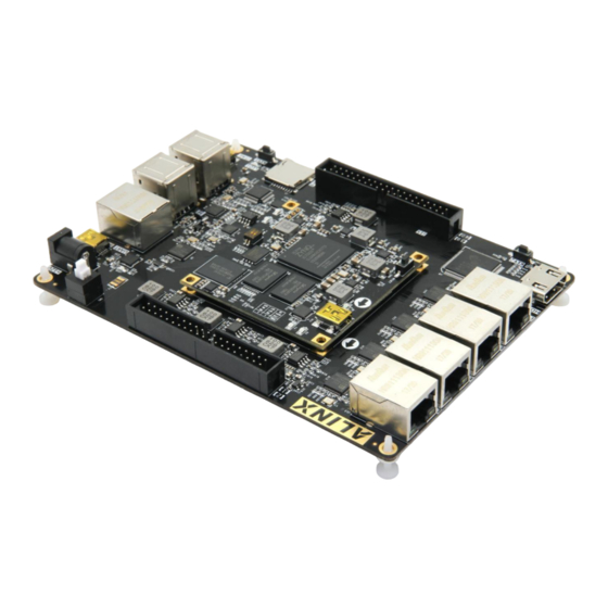
- Page 1 ZYNQ-7000 FPGA Development Board AX7021B User Manual...
-
Page 2: Version Record
AX7021B User Manual Version Record Version Date Release By Description Rev 1.0 2019-03-27 Rachel Zhou First Release Rev 1.1 2020-09-21 Rachel Zhou Correct the corresponding pins of B34_L15_N/P. 2 / 30 www.alinx.com... -
Page 3: Table Of Contents
AX7021B User Manual Version Record ................2 Part 2: AC7021B Core Board Introduction ......7 Part 2.1: ZYQN Chip ..............9 Part 2.2 DDR3 DRAM ............... 12 Part 2.3 QSPI Flash ..............14 Part 2.4: eMMC Flash ...............16 Part 2.5: Clock configuration ..........17 Part 2.6: USB to serial port ............. - Page 4 It is a "professional" ZYNQ development platform. For high-speed Ethernet data transmission and exchange, the pre-validation and post-application of data processing is possible. This product is very suitable for students, engineers and other groups engaged in ZYNQ development. 4 / 30 www.alinx.com...
- Page 5 HDMI output interface, 1-port SD Card interface, 1-port UART USB serial port interface, 1-port SD Card interface, 2-port 40-pin carrier headers and some button LEDs. Figure 1-1-1 is the block diagram of the FPGA development board AX7021B: 5 / 30 www.alinx.com...
- Page 6 PS end of the ZYNQ chip, and four Ethernet connections to the PL end of the ZYNQ chip. HDMI Output Display One HDMI output interface uses SIL9134 HDMI encoding chip of Silion Image Corporation, which supports up to 1080P@60Hz output and supports 3D 6 / 30 www.alinx.com...
-
Page 7: Part 2: Ac7021B Core Board Introduction
Part 2: AC7021B Core Board Introduction The AC7021B (core board model, the same below) core board is an FPGA development board based on the Zynq chip XC7Z020-2CLG484I of the XILINX ZYNQ7000 series. The ZYNQ chip's PS system integrates two ARM CortexTM- A9 processors, AMBA®... - Page 8 Moreover, the IOs connection part, the routing between the ZYNQ FPGA chip and the interface is equal length and differential processing. The core board size is only 2.36 inch* 2.36 inch, which is very suitable for secondary development. Figure: AC7021BCore board Front View 8 / 30 www.alinx.com...
-
Page 9: Part 2.1: Zyqn Chip
AX7021B User Manual Figure: AC7021B core board rear view Part 2.1: ZYQN Chip The development board uses Xilinx's Zynq7000 series chip, model XC7Z020-2CLG484I. The chip's PS system integrates two ARM CortexTM-A9 processors, AMBA® interconnects, internal memory, external memory interfaces and peripherals. These peripherals mainly include USB bus interface, Ethernet interface, SD/SDIO interface, I2C bus interface, CAN bus interface, UART interface, GPIO, etc. - Page 10 Two SD card, SDIO, MMC compatible controllers 2 SPIs, 2 UARTs, 2 I2C interfaces 4 groups of 32bit GPIO, 54 (32+22) as PS system IO, 64 connected to High bandwidth connection within PS and PS to PL 10 / 30 www.alinx.com...
- Page 11 XC7Z020-2CLG484I chip speed grade is -2, industrial grade, package is BGA484, pin pitch is 0.024 inch, the specific chip model definition of ZYNQ7000 series is shown in Figure 2-2 Figure 2-2: The Specific Chip Model Definition of ZYNQ7000 Series 11 / 30 www.alinx.com...
-
Page 12: Part 2.2 Ddr3 Dram
Figure 2-3: TheXC7Z020 chip used on the Core Board Part 2.2 DDR3 DRAM The AC7021B core board is equipped with two SK Hynix DDR3 SDRAM chips (1GB total), model H5TQ4G63AFR-PBI. The bus width of DDR3 SDRAM is 32 bits in total. DDR3 SDRAM has a maximum operating speed of 533MHz (data rate 1066Mbps). - Page 13 DDR3_DQS2_P PS_DDR_DQS_P2_502 DDR3_DQS2_N PS_DDR_DQS_N2_502 DDR3_DQS3_P PS_DDR_DQS_P3_502 DDR3_DQS4_N PS_DDR_DQS_N3_502 DDR3_D0 PS_DDR_DQ0_502 DDR3_D1 PS_DDR_DQ1_502 DDR3_D2 PS_DDR_DQ2_502 DDR3_D3 PS_DDR_DQ3_502 DDR3_D4 PS_DDR_DQ4_502 DDR3_D5 PS_DDR_DQ5_502 DDR3_D6 PS_DDR_DQ6_502 DDR3_D7 PS_DDR_DQ7_502 DDR3_D8 PS_DDR_DQ8_502 DDR3_D9 PS_DDR_DQ9_502 DDR3_D10 PS_DDR_DQ10_502 DDR3_D11 PS_DDR_DQ11_502 DDR3_D12 PS_DDR_DQ12_502 DDR3_D13 PS_DDR_DQ13_502 13 / 30 www.alinx.com...
-
Page 14: Part 2.3 Qspi Flash
DDR3_A14 PS_DDR_A14_502 DDR3_BA0 PS_DDR_BA0_502 DDR3_BA1 PS_DDR_BA1_502 DDR3_BA2 PS_DDR_BA2_502 DDR3_S0 PS_DDR_CS_B_502 DDR3_RAS PS_DDR_RAS_B_502 DDR3_CAS PS_DDR_CAS_B_502 DDR3_WE PS_DDR_WE_B_502 DDR3_ODT PS_DDR_ODT_502 DDR3_RESET PS_DDR_DRST_B_502 DDR3_CLK0_P PS_DDR_CKP_502 DDR3_CLK0_N PS_DDR_CKN_502 DDR3_CKE PS_DDR_CKE_502 Table 3-2: DDR3 DRAM Pin Assignment Part 2.3 QSPI Flash 14 / 30 www.alinx.com... - Page 15 ZYNQ chip. In the system design, the GPIO port functions of these PS ports need to be configured as the QSPI FLASH interface. Figure 4-1 shows the QSPI Flash in the schematic. Figure 4-1: QSPI Flash in the schematic 15 / 30 www.alinx.com...
-
Page 16: Part 2.4: Emmc Flash
FLASH is connected to the GPIO port of the BANK501 in the PS section of the ZYNQ chip. In the system design, the GPIO port functions of these PS ports need to be configured as the SD interface. Figure 5-1 shows the 16 / 30 www.alinx.com... -
Page 17: Part 2.5: Clock Configuration
MMC_CCLK PS_MIO48_501 MMC_CMD PS_MIO47_501 MMC_D0 PS_MIO46_501 MMC_D1 PS_MIO49_501 MMC_D2 PS_MIO50_501 MMC_D3 PS_MIO51_501 Table 5-2: Pin Assignment of eMMC FLASH Part 2.5: Clock configuration The AC7021B core board provides active clocks for the PS system and the 17 / 30 www.alinx.com... - Page 18 Table 6-1: PS Clock pin assignment PL system clock source The AC7021B core board provides a single-ended 50MHz PL system clock source with 3.3V power supply. The crystal output is connected to the global clock (MRCC) of the FPGA BANK13, which can be used to drive user logic within the FPGA.
-
Page 19: Part 2.6: Usb To Serial Port
Table 6-2: PL Clock pin assignment Part 2.6: USB to serial port For the AC7021B core board to work and debug separately, we have a Uart to USB interface for the core board. Used for separate power supply and debugging of the core board. The conversion chip uses the USB-UART chip of Silicon Labs CP2102GM. -
Page 20: Part 2.7: Led
Pin Number Explain UART_RXD PS_MIO14_500 Uart data output UART_TXD PS_MIO15_500 Uart data input Table 7-1: Uart Pin Assignment Part 2.7: LED There are 6 red LED lights on the AC7021B core board, one of which is the 20 / 30 www.alinx.com... - Page 21 LED light is off. When the connection IO voltage is low, the user LED will be illuminated. The schematic diagram of the LED light hardware connection is shown in Figure 8-1: Figure 8-1: The schematic diagram of the LED light hardware connection 21 / 30 www.alinx.com...
-
Page 22: Part 2.8: Reset Button
Table 8-1: LED Pin Assignment Part 2.8: Reset button The AC7021B has a reset button RESET and circuitry on the core board. The reset signal is connected to the PS reset pin of the ZYNQ chip. The reset button can be used by the user to reset the ZYNQ system. When the reset button is pressed, the reset chip will generate a low level reset signal to the ZYNQ chip. -
Page 23: Part 2.9: Jtage Interface
Table 9-1: Reset Pin Assignment Part 2.9: JTAGE Interface The JTAG test socket J1 is reserved on the AC7021B core board for separate JTAG download and debugging of the core board. Figure 10-1 is the schematic part of the JTAG port, which involves TMS, TDI, TDO, TCK, GND. , +3.3V these six signals. -
Page 24: Part 2.10: Dip Switch Configuration
Figure 10-2: JTAG interface on the core board Part 2.10: DIP switch configuration The AC7021B has a 2-digit DIP switch SW1 on the core board to configure the ZYNQ system's startup mode. The AC7021B system development platform supports three startup modes. The three startup modes are JTAG debug mode, QSPI FLASH and SD card boot mode. - Page 25 BANK33, 34 outputs a voltage standard of 2.5V. 1.5V generates the VTT and VREF voltages required by DDR3 through TI's TPS51200. The functions of each power distribution are shown in the following Table 12-1: 25 / 30 www.alinx.com...
- Page 26 +1.0V->+1.8V->(+1.5 V, +3.3V, VCCIO). The circuit design ensures the normal operation of the chip. The power supply on the core board detailed as Figure 12-2 below Figure 12-2: The Power Supply on the Core Board 26 / 30 www.alinx.com...
-
Page 27: Part 2.13: Connector Pin Definition
The IO levels of BANK33 and BANK34 can be changed by changing the level of the LDO chip (U12) on the board. The default is 3.3V. Pin assignment detailed as Table 14-1, Table 14-2, Table 14-3, Table 14-4: 27 / 30 www.alinx.com... - Page 28 Signal Name ZYNQ Pin ZYNQ Pin PS_MIO13 ETH_TXD0 PS_MIO12 ETH_TXD1 ETH_TXD2 ETH_TXD3 ETH_TXCK ETH_TXCTL ETH_RXD3 ETH_RXD2 PS_MIO7 ETH_RXD1 PS_MIO8 ETH_RXD0 PS_MIO9 ETH_RXCTL PS_MIO11 ETH_RXCK ETH_MDC ETH_MDIO OTG_STP OTG_DIR XADC_VP OTG_CLK XADC_VN OTG_NXT OTG_DATA0 PS_MIO10 OTG_DATA1 SD_CLK OTG_DATA2 28 / 30 www.alinx.com...
- Page 29 Singal Name B13_L1_N B33_L4_N B13_L1_P B33_L4_P B33_L10_P AB19 B33_L3_N B33_L10_N AB20 B33_L3_P B13_L4_N B33_L2_N B13_L4_P B33_L2_P B34_L6_N B13_L5_N B34_L6_P B13_L5_P B13_L12_N B33_IO25 B13_IO25 B34_IO25 B13_L23_N B13_L6_P B13_L23_P B13_L6_N B13_L13_N B13_L19_N B13_L13_P B13_L19_P B13_L24_N B13_L22_P B13_L24_P B13_L22_N 29 / 30 www.alinx.com...
- Page 30 B13_L17_N B13_L15_N B13_L17_P B13_L15_P B13_L21_N B13_L21_P Table 14-2: Pin Assignment of CON2 ZYNQ Pin ZYNQ Pin CON3 Pin Signal Name CON3 Pin Signal Name B34_L2_P B34_L12_N B34_L2_N B34_L12_P B34_L11_P B34_L10_N B34_L11_N B34_L10_P B34_L7_P B34_L3_N B34_L7_N B34_L3_P 30 / 30 www.alinx.com...
- Page 31 B33_L12_P B33_L16_N B33_L13_P B33_L17_N AB17 B33_L13_N B33_L17_P AA17 B33_L18_N AB16 B33_L7_P AA22 B33_L18_P AA16 B33_L7_N AB22 B33_L21_N B33_L19_N B33_L21_P B33_L19_P B33_L24_P AB14 B33_L15_N B33_L24_N AB15 B33_L15_P B33_L23_N AA13 B33_L14_P B33_L23_P B33_L14_N B33_L20_N B33_L22_P B33_L20_P B33_L22_N AA14 31 / 30 www.alinx.com...
- Page 32 B35_L11_P B35_L15_N B35_L13_N B35_L18_N B35_L13_P B35_L18_P B35_L14_N B35_L16_N B35_L14_P B35_L16_P B35_L12_P B35_L17_N B35_L12_N B35_L17_P B35_L2_N B35_L23_N B35_L2_P B35_L23_P B35_L1_N B35_L22_N B35_L1_P B35_L22_P B35_L21_P B34_L8_N B35_L21_N B34_L8_P B35_L24_P B35_L20_N B35_L24_N B35_L20_P B35_L6_P B35_L19_N B35_L6_N B35_L19_P B35_L4_P B34_L9_P 32 / 30 www.alinx.com...
-
Page 33: Part 3: Carrier Board
AX7021B User Manual B35_L4_N B34_L9_N B35_L3_N B35_IO25 B35_L3_P B35_IO0 B34_L24_N B34_L4_P B34_L24_P B34_L4_N B34_L23_P B34_L18_N B34_L23_N B34_L18_P B35_L5_P B34_L22_P B35_L5_N B34_L22_N B34_L19_P B34_L19_N Table 14-4: Pin Assignment of CON4 Part 3: Carrier Board 33 / 30 www.alinx.com... -
Page 34: Carrier Board Introduction
Mbps network transmission rate and data communication with the MAC layer of the Zynq7000 system through the RGMII interface. JL2121-N040IRNX supports MDI/MDX adaptation, various speed adaptive, Master/Slave adaptation, MDIO bus for PHY register management. After power-on, the JL2121-N040IRNX detects the level status of some 34 / 30 www.alinx.com... - Page 35 ZYNQ and PHY chip JL2121-N040IRNX is communicated through the RMII bus, and the transmission clock is 25Mhz. Data is sampled on the rising edge and falling samples of the clock. Figure 3-2-1 and Figure 3-2-2 detailed the connection of the ZYNQ chip end Ethernet PHY chip: 35 / 30 www.alinx.com...
- Page 36 AX7021B User Manual Figure 3-2-1: The connection of the ZYNQ PS end and PHY chip Figure 3-2-2: The connection of the 4 ZYNQ PL end and PHY chip 36 / 30 www.alinx.com...
- Page 37 PHY1_RXD0 PS_MIO23_501 Receive data Bit0 PHY1_RXD1 PS_MIO24_501 Receive data Bit1 PHY1_RXD2 PS_MIO25_501 Receive data Bit2 PHY1_RXD3 PS_MIO26_501 Receive data Bit3 PHY1_RXCTL PS_MIO27_501 Receive data valid signal PHY1_MDC PS_MIO52_501 MDIO Management clock PHY1_MDIO PS_MIO53_501 MDIO Management clock 37 / 30 www.alinx.com...
- Page 38 B33_L15_N Receive data Bit0 PHY4_RXD1 B33_L19_P Receive data Bit1 PHY4_RXD2 B33_L19_N Receive data Bit2 PHY4_RXD3 B33_L7_N AB22 Receive data Bit3 PHY4_RXCTL B33_L15_P Receive data valid signal PHY4_MDC B33_L14_N MDIO Management clock PHY4_MDIO B33_L22_P MDIO Management data 38 / 30 www.alinx.com...
-
Page 39: Usb2.0 Host Interface
USB Slave peripherals (such as USB mouse and USB keyboard) at the same time. The carrier board also provides +5V power to each USB interface The schematic diagram of the ZYNQ processor, USB3320C-EZK chip, USB2514 chip connection is shown as Figure 3-3-1 39 / 30 www.alinx.com... - Page 40 Figure 3-3-2: The USB2.0 on the Carrier Board USB2.0 Pin Assignment: Signal Name Pin Name Pin Number Explain OTG_DATA4 PS_MIO28_501 USB data bit4 USB data direction OTG_DIR PS_MIO29_501 signal OTG_STP PS_MIO30_501 USB stop signal OTG_NXT PS_MIO31_501 USB next data signal 40 / 30 www.alinx.com...
-
Page 41: Hdmi Output Interface
ZYNQ7000 PL part. The ZYNQ7000 system initializes and controls the SIL9134 through the I2C pin. The hardware connection diagram of SIL9134 chip and ZYNQ7000 is shown in Figure 3-4-1. Figure3-4-1: The hardware connection of SIL9134 chip and ZYNQ7000 41 / 30 www.alinx.com... - Page 42 9134_SPDIF B35_L1_N Audio S/PDIF input 9134_MCLK B35_L2_P Audio input master clock Audio interface I2S word 9134_WS B35_L14_N selection 9134_SD0 B35_L14_P Audio Interface I2S Data0 9134_SD1 B35_L12_P Audio Interface I2S Data1 9134_SD2 B35_L12_N Audio Interface I2S Data2 42 / 30 www.alinx.com...
-
Page 43: Usb To Serial Port
Figure 3-5-1 detailed the schematic diagram of the USB Uart circuit design. Figure 3-5-1: The Schematic Diagram of the USB Uart Circuit Figure 3-5-2: The UART on the Carrier Board 43 / 30 www.alinx.com... -
Page 44: Sd Card Slot
ZYNQ. Since the VCCMIO of the BANK is set to 1.8V, but the data level of the SD card is 3.3V, connected through the TXS02612 level shifter. The schematic of the Zynq7000 PS and SD card connector is shown in Figure 3-6-1 Figure 3-6-1: SD Card Connection Diagram 44 / 30 www.alinx.com... -
Page 45: Jtag Interface
On the AX7021B development board, the JTAG interface is in the USB interface mode. Users can connect the PC and JTAG interface to the ZYNQ system debugging through the USB cable provided by us. Figure 3-7-1: JTAG interface part of the schematic 45 / 30 www.alinx.com... -
Page 46: Led
LED is off, and when the connection IO voltage is low, the user LED is illuminated. The schematic diagram of the LED light hardware connection is shown in Figure 3-8-1: Figure 3-8-1: LED hardware connection Diagram on the Carrier Board 46 / 30 www.alinx.com... -
Page 47: User Button
ZYNQ chip detects a low level to determine whether the button is pressed. The schematic diagram of the user button connection is shown in Figure 3-9-1: Figure 3-9-1: The Schematic Diagram of the User Button 47 / 30 www.alinx.com... -
Page 48: Extension Port
3.10 Extension Port The AX7021B carrier board is reserved with two 2.54-mm standard 40-pin expansion ports J15 and J16 for connecting various modules of ALINX or external circuits designed by the user. The expansion port has 40 signals, of which 1 channel is 5V power supply. 2 channels are 3.3V power supplies, 3 Do not connect the IO directly to a 5V device to avoid Ground, 34 IOs. - Page 49 Figure 3-10-2 shows the physical map of the J15 expansion port. Pin39 and Pin40 of the expansion port are indicated on the board. Figure 3-10-2: The J15 Expansion Port on the Carrier Board J15 Pin Assignment: Signal Name Pin Name Pin Number +5V(Input) AA19 49 / 30 www.alinx.com...
- Page 50 AX7021B User Manual AB19 AB20 AA21 AB21 +3.3V +3.3V(Output) Figure 3-10-3: The Expansion Port J16 Schematic Figure 3-10-4: The J16 Expansion Port on the Carrier Board J16 Pin Assignment: Signal Name Pin Name Pin Number 50 / 30 www.alinx.com...
-
Page 51: Power Supply
BANK33 and BANK34 of the core board is replaced with other voltage levels, the output of this LDO chip on the carrier board needs to be modified accordingly. The power supply design on the carrier board is shown below 51 / 30 www.alinx.com... - Page 52 AX7021B User Manual Figure 3-11-1: Power Supply Schematic on the Carrier Board Figure 3-11-2: Power Supply on the Carrier Board (1.2V/5V/3.3V) Figure 3-11-3: Power Supply on the Carrier board (1.8V) 52 / 30 www.alinx.com...
-
Page 53: Carrier Board Structure Diagram
AX7021B User Manual 3.12 Carrier Board Structure diagram Figure 3-12-1: Carrier Board Structure Diagram 53 / 30 www.alinx.com...
Need help?
Do you have a question about the AC7021B and is the answer not in the manual?
Questions and answers