Table of Contents
Advertisement
Quick Links
Advertisement
Table of Contents

Related Manuals for Alinx AC7Z035B


Summary of Contents for Alinx AC7Z035B
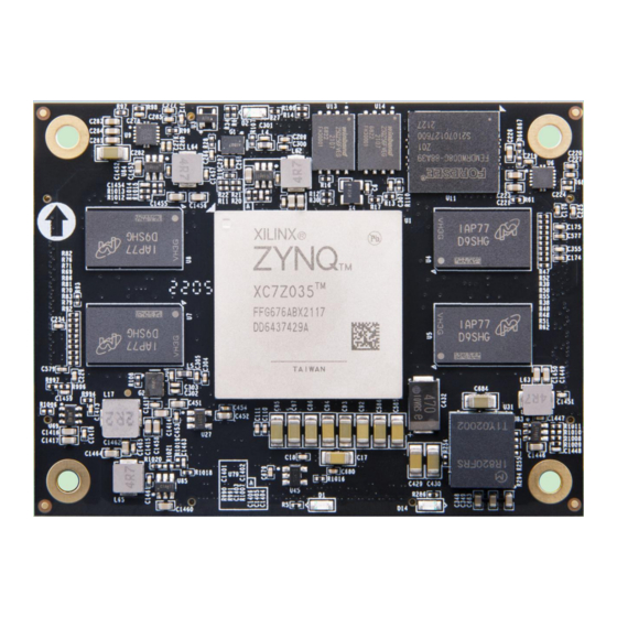
- Page 1 ZYNQ7000 FPGA Development Platform AC7Z035B System on Module...
-
Page 2: Version Record
2022-11-22 Rachel Zhou First Release The English version was translated by Shanghai Tianhui Trading Company. They has not been officially Review by ALINX and are for reference only. If there are any errors, please send email to rachel.zhou@aithtech.com for correction. -
Page 3: Table Of Contents
Part 6: Clock Configuration ................17 Part 7: LED Light ..................20 Part 8: Reset Circuit ...................21 Part 9: Power Supply ................. 22 Part 10: AC7Z035B Core Board Form Factors ......... 24 Part 11: Board to Board Connectors pin assignment ........24 Amazon Store: https://www.amazon.com/alinx... -
Page 4: Part 1: Ac7Z035B Core Board Introduction
ZYNQ FPGA Development Board AC7Z035B User Manual Part 1: AC7Z035B Core Board Introduction AC7Z035B (core board model, the same below) FPGA core board, ZYNQ chip is based on XC7Z035-2FFG676 of XILINX company ZYNQ7000 series. The ZYNQ chip's PS system integrates two ARM CortexTM-A9 processors, AMBA®... - Page 5 ZYNQ FPGA Development Board AC7Z035B User Manual Figure 1-1: AC7Z035B Core Board (Front View) Figure 1-2: AC7Z035B Core Board (Rear View) Amazon Store: https://www.amazon.com/alinx 5 / 32 Sales Email: rachel.zhou@aithtech.com...
-
Page 6: Part 2: Zynq Chip
ZYNQ FPGA Development Board AC7Z035B User Manual Part 2: ZYNQ Chip The FPGA core board AC7Z035B uses Xilinx's Zynq7000 series chip, model XC7Z035-2FFG676. The chip's PS system integrates two ARM CortexTM-A9 processors, AMBA® interconnects, internal memory, external memory interfaces and peripherals. These peripherals mainly include USB bus interface, Ethernet interface, SD/SDIO interface, I2C bus interface, CAN bus interface, UART interface, GPIO etc. - Page 7 ZYNQ FPGA Development Board AC7Z035B User Manual On-chip boot ROM and 256KB on-chip RAM External storage interface, support 16/32 bit DDR2, DDR3 interface Two Gigabit NIC support: divergent-aggregate DMA, GMII, RGMII, SGMII interface Two USB2.0 OTG interfaces, each supporting up to 12 nodes ...
- Page 8 ZYNQ FPGA Development Board AC7Z035B User Manual Figure 2-2: The Specific Chip Model Definition of ZYNQ7000 Series Figure 2-3: The XC7Z035 chip used on the Core Board Amazon Store: https://www.amazon.com/alinx 8 / 32 Sales Email: rachel.zhou@aithtech.com...
-
Page 9: Part 3: Ddr3 Dram
ZYNQ FPGA Development Board AC7Z035B User Manual Part 3: DDR3 DRAM The FPGA core board AC7Z035B is equipped with four Micron 512MB DDR3 chips, model MT41J256M16HA-125 (compatible with MT41K256M16HA-125), in which Two DDR3s are mounted on the PS and PL sides respectively. - Page 10 ZYNQ FPGA Development Board AC7Z035B User Manual Figure 3-1: The Schematic Part of DDR3 DRAM on the PS side Figure 3-2: The Schematic Part of DDR3 DRAM on the PL side PS side DDR3 DRAM pin assignment: Signal Name ZYNQ Pin Name...
- Page 11 ZYNQ FPGA Development Board AC7Z035B User Manual PS_DDR3_DQS3_P PS_DDR_DQS_P3_502 PS_DDR3_DQS4_N PS_DDR_DQS_N3_502 PS_DDR3_D0 PS_DDR_DQ0_502 PS_DDR3_D1 PS_DDR_DQ1_502 PS_DDR3_D2 PS_DDR_DQ2_502 PS_DDR3_D3 PS_DDR_DQ3_502 PS_DDR3_D4 PS_DDR_DQ4_502 PS_DDR3_D5 PS_DDR_DQ5_502 PS_DDR3_D6 PS_DDR_DQ6_502 PS_DDR3_D7 PS_DDR_DQ7_502 PS_DDR3_D8 PS_DDR_DQ8_502 PS_DDR3_D9 PS_DDR_DQ9_502 PS_DDR3_D10 PS_DDR_DQ10_502 PS_DDR3_D11 PS_DDR_DQ11_502 PS_DDR3_D12 PS_DDR_DQ12_502 PS_DDR3_D13 PS_DDR_DQ13_502 PS_DDR3_D14...
- Page 12 ZYNQ FPGA Development Board AC7Z035B User Manual PS_DDR3_DM2 PS_DDR_DM2_502 PS_DDR3_DM3 PS_DDR_DM3_502 PS_DDR3_A0 PS_DDR_A0_502 PS_DDR3_A1 PS_DDR_A1_502 PS_DDR3_A2 PS_DDR_A2_502 PS_DDR3_A3 PS_DDR_A3_502 PS_DDR3_A4 PS_DDR_A4_502 PS_DDR3_A5 PS_DDR_A5_502 PS_DDR3_A6 PS_DDR_A6_502 PS_DDR3_A7 PS_DDR_A7_502 PS_DDR3_A8 PS_DDR_A8_502 PS_DDR3_A9 PS_DDR_A9_502 PS_DDR3_A10 PS_DDR_A10_502 PS_DDR3_A11 PS_DDR_A11_502 PS_DDR3_A12 PS_DDR_A12_502 PS_DDR3_A13 PS_DDR_A13_502 PS_DDR3_A14...
- Page 13 ZYNQ FPGA Development Board AC7Z035B User Manual PL_DDR3_DQS1_N IO_L9N_T1_DQS_33 PL_DDR3_DQS2_P IO_L15P_T2_DQS_33 PL_DDR3_DQS2_N IO_L15N_T2_DQS_33 PL_DDR3_DQS3_P IO_L21P_T3_DQS_33 PL_DDR3_DQS4_N IO_L21N_T3_DQS_33 PL_DDR3_D0 IO_L5N_T0_33 PL_DDR3_D1 IO_L1N_T0_33 PL_DDR3_D2 IO_L4P_T0_33 PL_DDR3_D3 IO_L1P_T0_33 PL_DDR3_D4 IO_L2N_T0_33 PL_DDR3_D5 IO_L5P_T0_33 PL_DDR3_D6 IO_L2P_T0_33 PL_DDR3_D7 IO_L4N_T0_33 PL_DDR3_D8 IO_L7N_T1_33 PL_DDR3_D9 IO_L10N_T1_33 PL_DDR3_D10 IO_L7P_T1_33 PL_DDR3_D11...
-
Page 14: Part 4: Qspi Flash
PL_DDR3_RAS IO_L19P_T3_34 PL_DDR3_CAS IO_L20N_T3_34 PL_DDR3_WE IO_L20P_T3_34 PL_DDR3_ODT IO_L22P_T3_34 PL_DDR3_RESET IO_L16N_T2_34 PL_DDR3_CLK0_P IO_L21P_T3_DQS_34 PL_DDR3_CLK0_N IO_L21N_T3_DQS_34 PL_DDR3_CKE IO_L24P_T3_34 Part 4: QSPI Flash The FPGA core board AC7Z035B is equipped with two 256MBit Quad-SPI Amazon Store: https://www.amazon.com/alinx 14 / 32 Sales Email: rachel.zhou@aithtech.com... - Page 15 ZYNQ FPGA Development Board AC7Z035B User Manual FLASH chips to form an 8-bit bandwidth data bus, the flash model is W25Q256FVEI, which uses the 3.3V CMOS voltage standard. Due to the non-volatile nature of QSPI FLASH, it can be used as a boot device for the system to store the boot image of the system.
-
Page 16: Part 5: Emmc Flash
QSPI1_D3 PS_MIO13_500 Part 5: eMMC Flash The FPGA core board AC7Z035B is equipped with a large-capacity 8GB eMMC FLASH chip, model THGBMFG6C1LBAIL, which supports the JEDEC e-MMC V5.0 standard HS-MMC interface with level support of 1.8V or 3.3V. The data width of the eMMC FLASH and ZYNQ connections is 4 bits. Due to... -
Page 17: Part 6: Clock Configuration
ZYNQ FPGA Development Board AC7Z035B User Manual Figure 5-1: eMMC Flash in the Schematic Pin Assignment of eMMC Flash Signal Name ZYNQ Pin Name ZYNQ Pin Number MMC_CCLK PS_MIO48_501 MMC_CMD PS_MIO47_501 MMC_D0 PS_MIO46_501 MMC_D1 PS_MIO49_501 MMC_D2 PS_MIO50_501 MMC_D3 PS_MIO51_501 Part 6: Clock Configuration... - Page 18 The ZYNQ chip provides a 33.333MHz clock input to the PS section via the X4 crystal on the FPGA core board AC7Z035B. The input of the clock is connected to the pin of the PS_CLK_500 of the BANK500 of the ZYNQ chip.
- Page 19 PL system clock source The differential 200MHz PL system clock source is provided on the FPGA core board AC7Z035B for the reference clock of the DDR3 controller. The crystal output is connected to the global clock (MRCC) of the FPGA BANK34, which can be used to drive the DDR3 controller and user logic in the FPGA.
-
Page 20: Part 7: Led Light
BANK111_CLK1_N Part 7: LED Light There are 3 red LED lights on the AC7Z035B FPGA core board, one of which is the power indicator light (PWR), one is the configuration LED light (DONE), and one is the user LED light. When the core board is powered, the power indicator will illuminate;... -
Page 21: Part 8: Reset Circuit
User LED Light Part 8: Reset Circuit There is a reset circuit on the AC7Z035B core board. The reset input signal is connected to the reset button on the carrier board. The reset output is connected to the PS reset pin of the ZYNQ chip. The user can use the buttons on the carrier board to reset the ZYNQ system. -
Page 22: Part 9: Power Supply
PS_POR_B_500 ZYNQ System Reset Signal Part 9: Power Supply The AC7Z035B FPGA core board is powered by DC5V and is powered by a connection carrier board. The power supply design diagram on the FPGA board is shown in Figure 9-1 Figure 9-1:Power interface section in the schematic... - Page 23 ZYNQ FPGA Development Board AC7Z035B User Manual +5V generates +1.0V ZYNQ core power through DCDC power chip MYMGK1R820FRSR. The output current is up to 20A, which is enough to meet the current demand of ZYNQ core voltage. The +5V power supply then uses the DCDC chip ETA1471 to generate four power supplies: MGTAVTT, +1.5V,...
-
Page 24: Part 10: Ac7Z035B Core Board Form Factors
ZYNQ FPGA Development Board AC7Z035B User Manual Part 10: AC7Z035B Core Board Form Factors Figure 10-1: AC7Z035B Core Board Form Factors Part Board Board Connectors assignment The core board has a total of four high-speed expansion ports. It uses four 120-pin inter-board connectors (J29~J32) to connect to the carrier board. - Page 25 ZYNQ FPGA Development Board AC7Z035B User Manual B13_L8_P AE23 B13_L9_N AB22 B13_L8_N AF23 B13_L9_P AB21 B13_L10_N AA23 B13_L13_N AD21 B13_L10_P AA22 B13_L13_P AD20 B13_L15_N AF20 B13_L14_N AC22 B13_L15_P AF19 B13_L14_P AC21 B13_L23_N B13_L7_P AE22 B13_L23_P B13_L7_N AF22 B13_L22_P AA19 B13_L20_P...
- Page 26 ZYNQ FPGA Development Board AC7Z035B User Manual B12_L10_N AF13 B12_L19_P B12_L10_P AE13 B12_L19_N AA17 B12_L4_P AB11 B12_L20_P AB17 B12_L4_N AB10 B12_L20_N AB16 B12_L7_P AE10 B12_L8_N AF12 B12_L7_N AD10 B12_L8_P AE12 B12_L24_P B12_L21_P AC17 B12_L24_N B12_L21_N AC16 B12_L3_N AA10 B12_L17_P AE16...
- Page 27 ZYNQ FPGA Development Board AC7Z035B User Manual ZYNQ Pin ZYNQ Pin J30 Pin Signal Name J30 Pin Signal Name Number Number BANK112_TX0_N BANK112_RX0_N BANK112_TX0_P BANK112_RX0_P BANK112_TX1_N BANK112_RX1_N BANK112_TX1_P BANK112_RX1_P BANK112_TX2_N BANK112_RX2_N BANK112_TX2_P BANK112_RX2_P BANK112_TX3_N BANK112_RX3_N BANK112_TX3_P BANK112_RX3_P BANK112_CLK0_N BANK112_CLK1_N BANK112_CLK0_P...
- Page 28 ZYNQ FPGA Development Board AC7Z035B User Manual BANK111_RX3_N BANK111_RX3_P BANK111_TX3_N BANK111_TX3_P BANK111_RX2_N BANK111_RX2_P BANK111_TX2_N BANK111_TX2_P BANK111_RX1_N BANK111_RX1_P BANK111_TX1_N BANK111_TX1_P BANK111_RX0_N BANK111_RX0_P BANK111_TX0_N BANK111_TX0_P BANK111_CLK0_N BANK111_CLK0_P Pin assignment of J31 connector Amazon Store: https://www.amazon.com/alinx 28 / 32 Sales Email: rachel.zhou@aithtech.com...
- Page 29 ZYNQ FPGA Development Board AC7Z035B User Manual ZYNQ Pin ZYNQ Pin J31 Pin Signal Name J31 Pin Signal Name Number Number FPGA_TCK FPGA_TDI FPGA_TMS FPGA_TDO B35_L3_P B35_L2_P B35_L3_N B35_L2_N B35_L7_N B35_L6_P B35_L7_P B35_L6_N B35_L4_P B35_L23_P B35_L4_N B35_L23_N B35_L5_N B35_L22_P B35_L5_P...
- Page 30 ZYNQ FPGA Development Board AC7Z035B User Manual B35_L20_N B35_L18_P B35_L20_P B35_L18_N B35_L10_N B35_L15_N B35_L10_P B35_L15_P B35_L13_N B35_L13_P B35_L16_N B35_L16_P SYS_RESET Pin assignment of J32 connector Amazon Store: https://www.amazon.com/alinx 30 / 32 Sales Email: rachel.zhou@aithtech.com...
- Page 31 ZYNQ FPGA Development Board AC7Z035B User Manual ZYNQ Pin ZYNQ Pin J32 Pin Signal Name J32 Pin Signal Name Number Number PS_MIO5 PS_MIO17 PS_MIO4 PS_MIO18 PS_MIO14 PS_MIO19 PS_MIO15 PS_MIO20 PS_MIO52 PS_MIO16 PS_MIO53 PS_MIO21 PS_MIO7 PS_MIO26 PS_MIO25 PS_MIO40 PS_MIO24 PS_MIO41 PS_MIO23...
- Page 32 ZYNQ FPGA Development Board AC7Z035B User Manual PS_MIO28 PS_MIO37 PS_MIO38 PS_MIO39 B13_L1_P AA25 B13_L11_P AD23 B13_L1_N AB25 B13_L11_N AD24 B13_L6_P AA24 B13_L4_P AD25 B13_L6_N AB24 B13_L4_N AD26 B13_L2_N AC26 B13_L5_P AF24 B13_L2_P AB26 B13_L5_N AF25 B13_L12_P AC23 B13_L3_P AE25 B13_L12_N...
Need help?
Do you have a question about the AC7Z035B and is the answer not in the manual?
Questions and answers