Table of Contents
Advertisement
Quick Links
Advertisement
Table of Contents

Related Manuals for Alinx KINTEX-7 FPGA


Summary of Contents for Alinx KINTEX-7 FPGA
- Page 1 KINTEX-7 FPGA Development Board AV7K300 User Manual...
-
Page 2: Version Record
KINTEX-7 FPGA Development Board AV7K300 User Manual Version Record Version Date Release By Description Rev 1.0 2021-01-22 Rachel Zhou First Release Amazon Store: https://www.amazon.com/alinx 2 / 45... -
Page 3: Table Of Contents
KINTEX-7 FPGA Development Board AV7K300 User Manual Table of Contents Version Record.......................2 Part 1: FPGA Development Board Introduction..........5 Part 2: AC7K325 Core Board................8 Part 2.1: AC7K325 Core Board Introduction..........8 Part 2.2: FPGA Chip..................9 Part 2.3:DDR3 DRAM.................10 Part 2.4: QSPI Flash...................14 Part 2.5: Clock configuration.............. - Page 4 KINTEX-7 FPGA Development Board AV7K300 User Manual The AV7K300 FPGA development board, it is the XILINX KINTEX-7 FPGA development platform. The AV7K300 FPGA development platform uses XILINX's KINTEX-7 chip XC7K325 solution. The FPGA development board mounts four pieces of 512MB high-speed DDR3 SDRAM chips, and a 128Mb QSPI FLASH chip.
-
Page 5: Part 1: Fpga Development Board Introduction
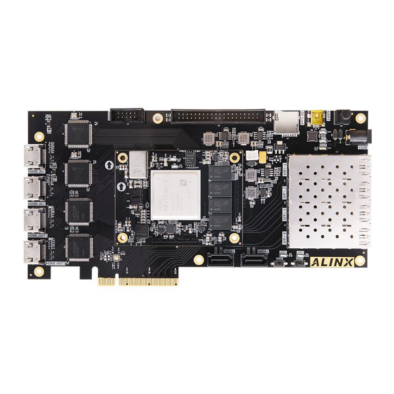
KINTEX-7 FPGA Development Board AV7K300 User Manual Part 1: FPGA Development Board Introduction The entire structure of the development board is designed by inheriting our usual core board + expansion board model. Use high-speed inter-board connectors to connect between the core board and the expansion board. - Page 6 KINTEX-7 FPGA Development Board AV7K300 User Manual Through this diagram, you can see the interfaces and functions that the AV7K300 FPGA Development Board contains: FPGA Core Board The smallest system consisting of XC7K325 + 4 DDR3 + QSPI FLASH,...
- Page 7 KINTEX-7 FPGA Development Board AV7K300 User Manual 1 Uart to USB interface, used for communication with computer, convenient for users to debug. The serial port chip adopts Silicon Labs CP2102GM USB-UART chip, and the USB interface adopts MINI USB interface.
-
Page 8: Part 2: Ac7K325 Core Board
KINTEX-7 FPGA Development Board AV7K300 User Manual Part 2: AC7K325 Core Board Part 2.1: AC7K325 Core Board Introduction AC7K325 (core board model, the same below) core board, FPGA chip is based on XC7K325TFFG900 of XILINX company XC7K325 series. The core board uses 4 Micron 512MB DDR3 chips MT41J256M16HA-125, with a total capacity of 2GB. -
Page 9: Part 2.2: Fpga Chip
XC7K325T-2FFG900I. The speed class is 2 and the temperature class is industrial. This model is a FGG900 package with 900 pins and a 1.0mm pitch. The chip naming rules for Xilinx KINTEX-7 FPGA are shown in Figure 2-2-1 below:... -
Page 10: Part 2.3:Ddr3 Dram
KINTEX-7 FPGA Development Board AV7K300 User Manual 16,020 Block RAM(kb) DSP48 Slices PCIe Gen2 XADC 12bit, 1Mbps AD GTP Transceiver 16,12.5Gb/s max Speed Grade Temperature Grade Industrial Part 2.3:DDR3 DRAM The AC7K325 FPGA core board is equipped with four 512MB DDR3 chips, model MT41K256M16HA-125 (Compatible with MT41J256M16HA-125). - Page 11 KINTEX-7 FPGA Development Board AV7K300 User Manual Figure 2-3-1: The DDR3 DRAM Schematic 4 DDR3 DRAM pin assignments: Signal Name FPGA Pin Name FPGA Pin DDR3_D0 IO_L13P_T2_MRCC_32 AD18 DDR3_D1 IO_L16N_T2_32 AB18 DDR3_D2 IO_L14P_T2_SRCC_32 AD17 DDR3_D3 IO_L17P_T2_32 AB19 DDR3_D4 IO_L14N_T2_SRCC_32 AD16...
- Page 12 KINTEX-7 FPGA Development Board AV7K300 User Manual DDR3_D14 IO_L10N_T1_32 AE19 DDR3_D15 IO_L11N_T1_SRCC_32 AG18 DDR3_D16 IO_L1N_T0_32 AK15 DDR3_D17 IO_L5N_T0_32 AJ17 DDR3_D18 IO_L2N_T0_32 AH15 DDR3_D19 IO_L4P_T0_32 AF15 DDR3_D20 IO_L4N_T0_32 AG14 DDR3_D21 IO_L5P_T0_32 AH17 DDR3_D22 IO_L2P_T0_32 AG15 DDR3_D23 IO_L1P_T0_32 AK16 DDR3_D24 IO_L19P_T3_32 AE15...
- Page 13 KINTEX-7 FPGA Development Board AV7K300 User Manual DDR3_D50 IO_L14N_T2_SRCC_34 DDR3_D51 IO_L13N_T2_MRCC_34 DDR3_D52 IO_L16P_T2_34 DDR3_D53 IO_L17N_T2_34 DDR3_D54 IO_L14P_T2_SRCC_34 DDR3_D55 IO_L17P_T2_34 DDR3_D56 IO_L2P_T0_34 DDR3_D57 IO_L4P_T0_34 DDR3_D58 IO_L1N_T0_34 DDR3_D59 IO_L6P_T0_34 DDR3_D60 IO_L5N_T0_34 DDR3_D61 IO_L5P_T0_34 DDR3_D62 IO_L2N_T0_34 DDR3_D63 IO_L4N_T0_34 DDR3_DM0 IO_L16P_T2_32 AA18 DDR3_DM1 IO_L12P_T1_MRCC_32...
-
Page 14: Part 2.4: Qspi Flash
KINTEX-7 FPGA Development Board AV7K300 User Manual DDR3_DQS7_P IO_L3P_T0_DQS_34 DDR3_DQS7_N IO_L3N_T0_DQS_34 DDR3_A0 IO_L1P_T0_33 AA12 DDR3_A1 IO_L1N_T0_33 AB12 DDR3_A2 IO_L2P_T0_33 DDR3_A3 IO_L2N_T0_33 DDR3_A4 IO_L3P_T0_DQS_33 DDR3_A5 IO_L3N_T0_DQS_33 DDR3_A6 IO_L6N_T0_VREF_33 AB13 DDR3_A7 IO_L4N_T0_33 DDR3_A8 IO_L5P_T0_33 AA11 DDR3_A9 IO_L5N_T0_33 AA10 DDR3_A10 IO_L6P_T0_33 AA13 DDR3_A11... - Page 15 KINTEX-7 FPGA Development Board AV7K300 User Manual configuration Bin files and other user data files in use. The specific models and related parameters of QSPI FLASH are shown in Table 2-4-1. Position Model Capacity Factory N25Q128 128M Bit Numonyx Table 2-4-1: QSPI FLASH Specification QSPI FLASH is connected to the dedicated pins of BANK0 and BANK14 of the FPGA chip.
-
Page 16: Part 2.5: Clock Configuration
KINTEX-7 FPGA Development Board AV7K300 User Manual Part 2.5: Clock configuration The core board provides 200Mhz and 125Mhz differential active clocks for the FPGA system. Provide differential clock sources for FPGA logic part and high-speed transceiver GTX part respectively. The schematic diagram of the... -
Page 17: Part 2.5.2: Gtx Reference Clock
KINTEX-7 FPGA Development Board AV7K300 User Manual Figure 2-5-2: 200Mhz System Clock Source Schematic System Clock pin assignments: Signal Name FPGA Pin SYS_CLK_P AE10 SYS_CLK_N AF10 Part 2.5.2: GTX Reference Clock The AC7K325 core board provides a 125Mhz reference clock for the GTX transceiver. -
Page 18: Part 2.6: Led Light
KINTEX-7 FPGA Development Board AV7K300 User Manual Figure 2-5-3: GTX Clock Source GTX Clock Source FPGA pin assignments: Signal Name FPGA Pin BANK117_CLK1_P BANK117_CLK1_N Part 2.6: LED Light There are 2 red LED lights on the AC7K325 core board, one of which is the power indicator (PWR) and the other is the configuration LED (DONE). -
Page 19: Part 2.7: Power Supply
KINTEX-7 FPGA Development Board AV7K300 User Manual Figure 2-6-1: LED in core board Schematic Part 2.7: Power Supply The AC7K325 core board power supply voltage is DC5V, which is powered by the carrier board. The core board power supply schematic is show as Figure 2-7-1. - Page 20 KINTEX-7 FPGA Development Board AV7K300 User Manual Figure 2-7-1: Power Supply Design Diagram +5V generates +1.0V FPGA core power through the DCDC power chip EM2130L01QI. The output current of EM2130 is up to 20A, which meets the current demand of the core voltage. The +5V power supply then generates +1.5V, +3.3V, MGT_1.5V and +1.5V four-way power supply through the DCDC...
- Page 21 KINTEX-7 FPGA Development Board AV7K300 User Manual chip TPS82085. The +1.0V used by the GTX transceiver is generated by the DCDC chip EN6362QI, and the MGT_1.5V power supply is generated by the LDO chip TPS74401 to generate the +1.2V power supply required by GTX.
-
Page 22: Part 2.8: Size Dimension
KINTEX-7 FPGA Development Board AV7K300 User Manual Part 2.8: Size Dimension Figure 2-8-1: AC7K325 Core Board Size Dimension Part 2.9: Board-to-Board Pin Definition The core board expands a total of 4 high-speed expansion ports, using 4 120-Pin inter-board connectors (J29~J32) to connect to the carrier board. The... - Page 23 KINTEX-7 FPGA Development Board AV7K300 User Manual J29 connector pin assignment J29 Pin Signal Name FPGA Pin J29 Pin Signal Name FPGA Pin BANK115_TX0_N BANK115_RX0_N BANK115_TX0_P BANK115_RX0_P BANK115_TX1_N BANK115_RX1_N BANK115_TX1_P BANK115_RX1_P BANK115_TX2_N BANK115_RX2_N BANK115_TX2_P BANK115_RX2_P BANK115_TX3_N BANK115_RX3_N BANK115_TX3_P BANK115_RX3_P BANK115_CLK0_N...
- Page 24 KINTEX-7 FPGA Development Board AV7K300 User Manual BANK117_TX0_N BANK118_TX0_N BANK117_TX0_P BANK118_TX0_P BANK117_RX0_N BANK118_RX0_N BANK117_RX0_P BANK118_RX0_P BANK117_TX1_N BANK118_TX1_N BANK117_TX1_P BANK118_TX1_P BANK117_RX1_N BANK118_RX1_N BANK117_RX1_P BANK118_RX1_P BANK117_TX2_N BANK118_TX2_N BANK117_TX2_P BANK118_TX2_P BANK117_RX2_N BANK118_RX2_N BANK117_RX2_P BANK118_RX2_P BANK117_TX3_N BANK118_TX3_N BANK117_TX3_P BANK118_TX3_P BANK117_RX3_N BANK118_RX3_N BANK117_RX3_P BANK118_RX3_P BANK117_CLK0_N...
- Page 25 KINTEX-7 FPGA Development Board AV7K300 User Manual J30 connector pin assignment J30 Pin Signal Name FPGA Pin J30 Pin Signal Name FPGA Pin B18_L5_P B18_L3_P B18_L5_N B18_L3_N B18_L6_P B18_L2_P B18_L6_N B18_L2_N B18_L7_P B18_L1_P B18_L7_N B18_L1_N B18_L8_P B18_L4_P B18_L8_N B18_L4_N B18_L9_P...
- Page 26 KINTEX-7 FPGA Development Board AV7K300 User Manual B17_L17_P B17_L14_P B17_L17_N B17_L14_N B17_L1_P B17_L20_P B17_L1_N B17_L20_N B17_L22_N B17_L21_P B17_L22_P B17_L21_N B17_L8_P B17_L13_P B17_L8_N B17_L13_N B17_L24_P B17_L23_N B17_L24_N B17_L23_P B17_L18_N B17_L12_P B17_L18_P B17_L12_N B17_L19_N B17_L11_N B17_L19_P B17_L11_P B17_L10_N B17_L9_N B17_L10_P B17_L9_P B17_L16_N...
- Page 27 KINTEX-7 FPGA Development Board AV7K300 User Manual J31 connector pin assignment J31 Pin Signal Name FPGA Pin J31 Pin Signal Name FPGA Pin B16_L12_N B16_L8_P B16_L12_P B16_L8_N B16_L10_N B16_L16_N B16_L10_P B16_L16_P B16_L11_N B16_L7_N B16_L11_P B16_L7_P B16_L13_N B16_L18_N B16_L13_P B16_L18_P B16_L21_P...
- Page 28 KINTEX-7 FPGA Development Board AV7K300 User Manual B15_L14_N B15_L7_N B15_L14_P B15_L7_P B15_L10_N B15_L8_N B15_L10_P B15_L8_P B15_L1_N B15_L24_N B15_L1_P B15_L24_P B15_L18_N B15_L3_N B15_L18_P B15_L3_P B15_L2_N B15_L21_N B15_L2_P B15_L21_P B15_L13_P B15_L12_N B15_L13_N B15_L12_P B15_L22_N B15_L20_N B15_L22_P B15_L20_P B15_L15_N B15_L9_N B15_L15_P B15_L9_P B15_L19_N...
- Page 29 KINTEX-7 FPGA Development Board AV7K300 User Manual J32 connector pin assignment J32 Pin Signal Name FPGA Pin J32 Pin Signal Name FPGA Pin B13_L16_P AE30 B13_L10_N AB30 B13_L16_N AF30 B13_L10_P AB29 B13_L23_N AF27 B13_L9_P AD29 B13_L23_P AF26 B13_L9_N AE29 B13_L14_P...
- Page 30 KINTEX-7 FPGA Development Board AV7K300 User Manual B12_L12_P AD23 B12_L9_N AD24 B12_L12_N AE24 B12_L9_P AC24 B12_L16_P AE25 B12_L8_N AD22 B12_L16_N AF25 B12_L8_P AC22 B12_L13_P AF22 B12_L7_N AC25 B12_L13_N AG23 B12_L7_P AB24 B12_L18_P AG25 B12_L4_N AA23 B12_L18_N AH25 B12_L4_P AA22 B12_L15_N...
-
Page 31: Part 3: Carrier Board
KINTEX-7 FPGA Development Board AV7K300 User Manual Part 3: Carrier Board Part 3.1: Carrier Board Introduction Through the previous function introduction, we can understand the function of the carrier board 4 optical fiber interface 1 PCIEx8 interface 2 channels of SDI video output interface supporting 3G ... - Page 32 KINTEX-7 FPGA Development Board AV7K300 User Manual Figure 3-2-1: Optical Fiber Design Schematic 4-channel SFP Interface FPGA pin assignment is as follows: Signal Name FPGA Pin Description Number SFP1_TX_P BANK117_TX0_P SFP 1 Data Transmitter (Positive) SFP1_TX_N BANK117_TX0_N SFP 1 Data Transmitter (Negative)
-
Page 33: Part 3.3.: Pcie Card Slot
KINTEX-7 FPGA Development Board AV7K300 User Manual SFP4_RX_P BANK117_RX3_P SFP 4 Data Receiver (Positive) SFP4_RX_N BANK117_RX3_N SFP 4 Data Receiver (Negative) BANK117_CLK1_P BANK117_CLK1_P Transceiver reference clock positive BANK117_CLK1_N BANK117_CLK1_N Transceiver reference clock negative Part 3.3.: PCIe Card Slot The AV7K300 FPGA development board provides an industrial-grade high-speed data transfer PCIe x8 interface. - Page 34 KINTEX-7 FPGA Development Board AV7K300 User Manual Figure 3-3-1: PCIe Slot Design Schematic PCIex8 Interface Pin Assignment: Signal Name FPGA Pin Description Number PCIE_RX0_P BANK116_RX3_P PCIE Channel 0 Data Receive Positive PCIE_RX0_N BANK116_RX3_N PCIE Channel 0 Data Receive Negative PCIE_RX1_P...
-
Page 35: Part 3.4: Sdi Output Interface
KINTEX-7 FPGA Development Board AV7K300 User Manual PCIE_RX5_P BANK115_RX2_P PCIE Channel 5 Data Receive Positive PCIE_RX5_N BANK115_RX2_N PCIE Channel 5 Data Receive Negative PCIE_RX6_P BANK115_RX1_P PCIE Channel 6 Data Receive Positive PCIE_RX6_N BANK115_RX1_N PCIE Channel 6 Data Receive Negative PCIE_RX7_P... - Page 36 KINTEX-7 FPGA Development Board AV7K300 User Manual GTX transceiver TX of FPGA BANK118 to realize high-speed SDI video output. The hardware connection diagram of GV8500 chip and FPGA is shown in Figure 3-4-1: Figure 3-4-1: SDI Output Interface Schematic The pin assignment of the 1...
-
Page 37: Part 3.5: Sdi Input Interface
KINTEX-7 FPGA Development Board AV7K300 User Manual Part 3.5: SDI Input Interface There are 2 SDI input interfaces on the carrier board, used GV8500 SDI equalizer chips, which supports different formats of data input HDcctv 1.0, HD-SDI (ST 292), 3G_SDI (ST-424) and SD_SDI (ST259). The input interface is adaptive to video reception at three rates. -
Page 38: Part 3.6: Usb To Serial Port
KINTEX-7 FPGA Development Board AV7K300 User Manual Signal Name FPGA Pin Description Number SDI2_3G_RXN BANK118_RX1_N SDI Input Differential Signal Negative SDI2_3G_RXP BANK118_RX1_P SDI Input Differential Signal Positive Part 3.6: USB to Serial Port The AV7K300 carrier board is equipped with a Uart to USB interface for system debugging. -
Page 39: Part 3.9: 40-Pin Expansion Port
KINTEX-7 FPGA Development Board AV7K300 User Manual interface to provide users with access to SD card memory for storing pictures, music or other user data files. SDIO signal is connected with FPGA IO signal, supports SPI mode and SD mode, the SD card used is MicroSD card. The schematic diagram of FPGA and SD card connector is shown in Figure 3-7-1. - Page 40 KINTEX-7 FPGA Development Board AV7K300 User Manual spacing standard 40-pin expansion port J18, J33, which are used to connect the ALINX modules or the external circuit designed by the user. The expansion port has 40 signals, of which 1-channel 5V power supply, 2-channel 3.3 V power supply, 3-channle ground and 34 IOs.
-
Page 41: Part 3.9: Keys And Leds
KINTEX-7 FPGA Development Board AV7K300 User Manual J33 Expansion Header Pin Assignment J33 Pin Signal Name J33 Pin Signal Name Number Number IO2_1N IO2_1P IO2_2N IO2_2P IO2_3N IO2_3P IO2_4N IO2_4P IO2_5N IO2_5P IO2_6N IO2_6P IO2_7N IO2_7P IO2_8N IO2_8P IO2_9N IO2_9P... - Page 42 KINTEX-7 FPGA Development Board AV7K300 User Manual user LED will be extinguished. In addition, there are 4 user buttons on the board. The default button signal is high. When the button is pressed, the button level is low. The hardware connection diagram of user LED lights and buttons is...
-
Page 43: Part 3.10: Jtag Debug Port
KINTEX-7 FPGA Development Board AV7K300 User Manual KEY1 B12_L19_N User KEY1 AF21 KEY2 B12_11_N User KEY2 AF23 B12_L3_P KEY3 User KEY3 AB22 KEY4 B12_L5_P User KEY4 AC20 Part 3.10: JTAG debug port A JTAG interface is reserved JTAG interface one the AV7K300 FPGA development board for downloading FPGA programs or firmware to FLASH. - Page 44 KINTEX-7 FPGA Development Board AV7K300 User Manual into +5V, +3.3V two-way power supply through 1 way DC/DC power chip TPS54620 and 1 way DC/DC power chip MP1482. Because the +5V power supply supplies power to the core board through the inter-board connector, the current output of the DCDC power supply is 6A, and the current output of the other 3.3V is 2A.
-
Page 45: Part 3.12: Size Dimension
KINTEX-7 FPGA Development Board AV7K300 User Manual Part 3.12: Size Dimension Figure 3-12-1: Carrier Board Size Dimension Amazon Store: https://www.amazon.com/alinx 45 / 45...
Need help?
Do you have a question about the KINTEX-7 FPGA and is the answer not in the manual?
Questions and answers