Table of Contents
Advertisement
Quick Links
Advertisement
Table of Contents

Related Manuals for Alinx ACU15EG


Summary of Contents for Alinx ACU15EG
- Page 1 ZYNQ UltraScale+ MPSoC FPGA Core Board ACU15EG User Manual...
-
Page 2: Version Record
ZYNQ Ultrascale + FPGA Board ACU15EG User Manual Version Record Version Date Release By Description Rev 1.1 2021-06-24 Rachel Zhou First Release www.alinx.com 2 / 30... -
Page 3: Table Of Contents
ZYNQ Ultrascale + FPGA Board ACU15EG User Manual Table of Contents Version Record .....................2 ACU15EG Core Board .................4 Part 1: ACU15EG Core Board Introduction .......... 4 Part 2: ZYNQ Chip ................5 Part 3: DDR4 DRAM ................7 Part 4: QSPI Flash ................14 Part 5: eMMC Flash ................ -
Page 4: Acu15Eg Core Board
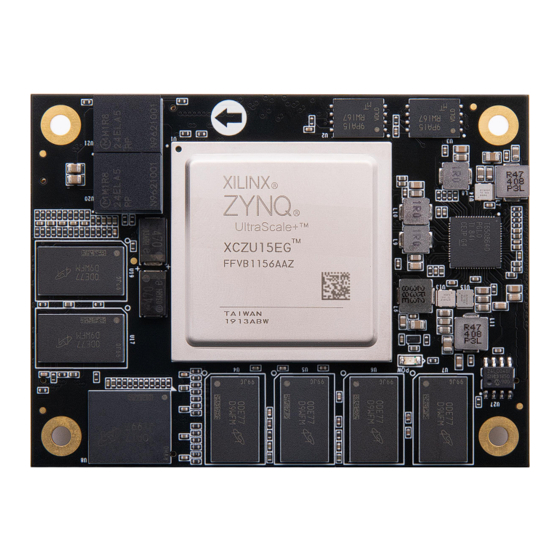
ZYNQ Ultrascale + FPGA Board ACU15EG User Manual ACU15EG Core Board Part 1: ACU15EG Core Board Introduction ACU15EG (core board model, the same below) FPGA core board, ZYNQ chip is based on XCZU15EG-2FFVB1156I of XILINX company Zynq UltraScale+ MPSoCs EG Family. -
Page 5: Part 2: Zynq Chip
Figure 2-1-1: ACU15EG Core Board (Front View) Part 2: ZYNQ Chip The FPGA core board ACU15EG uses Xilinx's Zynq UltraScale+ MPSoCs EG family chip, module XCZU15EG-2FFVB1156I. The PS system of the ZU15EG chip integrates 4 ARM Cortex™-A53 processors with a speed of up to 1.3Ghz and supports Level 2 Cache;... - Page 6 ZYNQ Ultrascale + FPGA Board ACU15EG User Manual Figure 2-2-1 detailed the Overall Block Diagram of the ZU15EG Chip. Figure 2-2-1: Overall Block Diagram of the ZYNQ ZU15EG Chip The main parameters of the PS system part are as follows: ...
-
Page 7: Part 3: Ddr4 Dram
FFVB1156. Part 3: DDR4 DRAM The ACU15EG core board is equipped with 6 Micron (Micron) 1GB DDR4 chips, model MT40A512M16LY-062E, of which 4 DDR4 chips are mounted on the PS side to form a 64-bit data bus bandwidth and 4GB capacity. Two DDR4 chip is mounted on the PL end, which is a 32-bit data bus width and a capacity of 2GB. - Page 8 ZYNQ Ultrascale + FPGA Board ACU15EG User Manual can reach 1200MHz (data rate 2400Mbps), and the 4 DDR4 storage systems are directly connected to the memory interface of the PS BANK504. The highest operating speed of the DDR4 SDRAM on the PL side can reach 1200MHz (data rate 2400Mbps), and two piece of DDR4 is connected to the BANK64,65 interface of the FPGA.
- Page 9 ZYNQ Ultrascale + FPGA Board ACU15EG User Manual Figure 2-3-2: Figure 2-3-2: DDR4 DRAM schematic diagram PS Side DDR4 DRAM pin assignment: Signal Name Pin Name Pin Number PS_DDR4_DQS0_N PS_DDR_DQS_N0_504 AN19 PS_DDR4_DQS0_P PS_DDR_DQS_P0_504 AN18 PS_DDR4_DQS1_N PS_DDR_DQS_N1_504 AN22 PS_DDR4_DQS1_P PS_DDR_DQS_P1_504 AN21...
- Page 10 ZYNQ Ultrascale + FPGA Board ACU15EG User Manual PS_DDR4_DQ0 PS_DDR_DQ0_504 AP20 PS_DDR4_DQ1 PS_DDR_DQ1_504 AP18 PS_DDR4_DQ2 PS_DDR_DQ2_504 AP19 PS_DDR4_DQ3 PS_DDR_DQ3_504 AP17 PS_DDR4_DQ4 PS_DDR_DQ4_504 AM20 PS_DDR4_DQ5 PS_DDR_DQ5_504 AM19 PS_DDR4_DQ6 PS_DDR_DQ6_504 AM18 PS_DDR4_DQ7 PS_DDR_DQ7_504 AL18 PS_DDR4_DQ8 PS_DDR_DQ8_504 AP22 PS_DDR4_DQ9 PS_DDR_DQ9_504 AP21 PS_DDR4_DQ10 PS_DDR_DQ10_504...
- Page 11 ZYNQ Ultrascale + FPGA Board ACU15EG User Manual PS_DDR4_DQ36 PS_DDR_DQ36_504 AJ30 PS_DDR4_DQ37 PS_DDR_DQ37_504 AK29 PS_DDR4_DQ38 PS_DDR_DQ38_504 AK30 PS_DDR4_DQ39 PS_DDR_DQ39_504 AJ29 PS_DDR4_DQ40 PS_DDR_DQ40_504 AE27 PS_DDR4_DQ41 PS_DDR_DQ41_504 AF28 PS_DDR4_DQ42 PS_DDR_DQ42_504 AF30 PS_DDR4_DQ43 PS_DDR_DQ43_504 AF31 PS_DDR4_DQ44 PS_DDR_DQ44_504 AD28 PS_DDR4_DQ45 PS_DDR_DQ45_504 AD27 PS_DDR4_DQ46 PS_DDR_DQ46_504...
- Page 12 ZYNQ Ultrascale + FPGA Board ACU15EG User Manual PS_DDR4_A0 PS_DDR_A0_504 AP29 PS_DDR4_A1 PS_DDR_A1_504 AP30 PS_DDR4_A2 PS_DDR_A2_504 AP26 PS_DDR4_A3 PS_DDR_A3_504 AP27 PS_DDR4_A4 PS_DDR_A4_504 AP25 PS_DDR4_A5 PS_DDR_A5_504 AN24 PS_DDR4_A6 PS_DDR_A6_504 AM29 PS_DDR4_A7 PS_DDR_A7_504 AM28 PS_DDR4_A8 PS_DDR_A8_504 AM26 PS_DDR4_A9 PS_DDR_A9_504 AM25 PS_DDR4_A10 PS_DDR_A10_504...
- Page 13 ZYNQ Ultrascale + FPGA Board ACU15EG User Manual PL_DDR4_DQS1_P IO_L16P_T2U_N6_QBC_AD3P_65 PL_DDR4_DQS2_N IO_L10N_T1U_N7_QBC_AD4N_65 PL_DDR4_DQS2_P IO_L10P_T1U_N6_QBC_AD4P_65 PL_DDR4_DQS3_N IO_L4N_T0U_N7_DBC_AD7N_65 PL_DDR4_DQS3_P IO_L4P_T0U_N6_DBC_AD7P_65 AG11 PL_DDR4_DQ0 IO_L24P_T3U_N10 _I2C_SDA_65 PL_DDR4_DQ1 IO_L20P_T3L_N2_AD1P_65 PL_DDR4_DQ2 IO_L23N_T3U_N9_65 PL_DDR4_DQ3 IO_L21P_T3L_N4_AD8P_65 PL_DDR4_DQ4 IO_L23P_T3U_N8_I2C_SCLK_65 PL_DDR4_DQ5 IO_L20N_T3L_N3_AD1N_65 PL_DDR4_DQ6 IO_L24N_T3U_N11_PERSTN0_65 PL_DDR4_DQ7 IO_L21N_T3L_N5_AD8N_65 PL_DDR4_DQ8 IO_L17P_T2U_N8_AD10P_65 PL_DDR4_DQ9 IO_L15P_T2L_N4_AD11P_65...
-
Page 14: Part 4: Qspi Flash
IO_L16N_T2U_N7_QBC_AD3N_64 PL_DDR4_WE_B IO_L9P_T1L_N4_AD12P_64 PL_DDR4_ACT_B IO_L8P_T1L_N2_AD5P_64 PL_DDR4_CS_B IO_L17N_T2U_N9_AD10N_64 PL_DDR4_CKE IO_L6N_T0U_N11_AD6N_64 AK10 PL_DDR4_OTD IO_L9N_T1L_N5_AD12N_64 PL_DDR4_BG0 IO_L3P_T0L_N4_AD15P_64 AL10 PL_DDR4_CLK_N IO_L13N_T2L_N1_GC_QBC_64 PL_DDR4_CLK_P IO_L13P_T2L_N0_GC_QBC_64 PL_DDR4_RST IO_L14N_T2L_N3_GC_64 Part 4: QSPI Flash The FPGA core board ACU15EG is equipped with two 256MBit Quad-SPI www.alinx.com 14 / 30... - Page 15 ZYNQ Ultrascale + FPGA Board ACU15EG User Manual FLASH chip to form an 8-bit bandwidth data bus, the flash model is MT25QU256ABA1EW9, which uses the 1.8V CMOS voltage standard. Due to the non-volatile nature of QSPI FLASH, it can be used as a boot device for the system to store the boot image of the system.
-
Page 16: Part 5: Emmc Flash
PS_MIO11_500 AF17 Part 5: eMMC Flash The ACU15EG core board is equipped with a large-capacity 8GB eMMC FLASH chip, the model is MTFC8GAKAJCN-4M, it supports the HS-MMC interface of the JEDEC e-MMC V5.0 standard, and the level supports 1.8V or 3.3V. -
Page 17: Part 6: Clock Configuration
ZYNQ Ultrascale + FPGA Board ACU15EG User Manual Figure 2-5-1: eMMC Flash in the schematic Configuration Chip pin assignment: Signal Name Pin Name Pin Number MMC_CCLK PS_MIO22_500 AD20 MMC_CMD PS_MIO21_500 AF18 MMC_DAT0 PS_MIO13_500 AK17 MMC_DAT1 PS_MIO14_500 AL16 MMC_DAT2 PS_MIO15_500 AN16... - Page 18 ZYNQ Ultrascale + FPGA Board ACU15EG User Manual Figure 2-6-1: Core Board Clock Source PS System RTC Real Time Clock The passive crystal Y1 on the core board provides a 32.768KHz real-time clock source for the PS system. The crystal is connected to the PS_PADI_503 and PS_PADO_503 pins of BANK503 of the ZYNQ chip.
- Page 19 ZYNQ Ultrascale + FPGA Board ACU15EG User Manual PS System Clock Source The X1 crystal on the core board provides a 33.333MHz clock input for the PS part. The clock input is connected to the PS_REF_CLK_503 pin of BANK503 of the ZYNQ chip. The schematic diagram is shown in Figure 2-6-3:...
-
Page 20: Part 7: Power Supply
PL_CLK0_N Part 7: Power Supply The power supply voltage of the ACU15EG core board is DC12V, which is supplied by connecting the carrier board. The core board uses 2 MYMGM1R824 power chips in parallel to achieve a 50A current to provide the core power of the XCZU15EG with 0.85V. - Page 21 ZYNQ Ultrascale + FPGA Board ACU15EG User Manual www.alinx.com 21 / 30...
-
Page 22: Part 8: Acu15Eg Core Board Size Dimension
ZYNQ Ultrascale + FPGA Board ACU15EG User Manual Part 8: ACU15EG Core Board Size Dimension Figure 2-8-1: ACU15EG Core Board Size Dimension Part 10: Board to Board Connectors pin assignment The core board has a total of four high-speed expansion ports. It uses four 120-pin inter-board connectors (J29/J30/J31/J32) to connect to the carrier board. - Page 23 ZYNQ Ultrascale + FPGA Board ACU15EG User Manual J29 Pin Signal Name J29 Pin Signal Name Pin Number Number B66_L3_P AA11 B67_L1_P B66_L3_N AA10 B67_L1_N B66_L2_P AB11 B66_L7_P B66_L2_N AB10 B66_L7_N B66_L5_N AA12 B66_L8_P B66_L5_P B66_L8_N B67_L2_N B66_L1_N AC11 B67_L2_P...
- Page 24 ZYNQ Ultrascale + FPGA Board ACU15EG User Manual B67_L23_P B67_L17_N B67_L7_N B67_L13_P B67_L7_P B67_L13_N B67_L9_P B66_L23_N B67_L9_N B66_L23_P B67_L18_P B67_L12_P B67_L18_N B67_L12_N B67_L10_P B67_L14_P B67_L10_N B67_L14_N 228_RX1_N 228_RX0_N 228_RX1_P 228_RX0_P 228_TX1_N 228_TX0_N 228_TX1_P 228_TX0_P 228_RX3_N 228_RX2_N 228_RX3_P 228_RX2_P 228_TX3_N 228_TX2_N...
- Page 25 ZYNQ Ultrascale + FPGA Board ACU15EG User Manual 505_RX0_P AB33 505_TX3_P 505_RX0_N AB34 505_TX3_N 505_CLK1_P 505_TX2_P 505_CLK1_N 505_TX2_N 505_RX2_N 505_CLK2_P 505_RX2_P 505_CLK2_N 505_RX3_P 505_RX1_N AA32 505_RX3_N 505_RX1_P AA31 505_CLK3_P 505_TX1_N 505_CLK3_N 505_TX1_P PS_MIO26 USB_STP PS_MIO35 USB_DIR PS_MIO28 USB_CLK PS_MIO37 USB_NXT...
- Page 26 ZYNQ Ultrascale + FPGA Board ACU15EG User Manual PS_MIO41 PHY1_TXD3 PS_MIO44 PHY1_TXCK SD_CD PHY1_TXCTL SD_D0 PHY1_RXD3 SD_D3 PHY1_RXD2 SD_D1 PHY1_RXD1 SD_D2 PHY1_RXD0 SD_CLK PHY1_RXCTL SD_CMD PHY1_RXCK VCCO_66 VCCO_67 VCCO_66 VCCO_67 +12V +12V +12V +12V +12V +12V +12V +12V +12V +12V...
- Page 27 ZYNQ Ultrascale + FPGA Board ACU15EG User Manual PS_MODE1 VBAT_IN PS_MODE0 PS_POR_B PS_ERROR_STATU FPGA_DONE PS_ERROR_OUT B44_L5_P AK15 B50_L11_N B44_L5_N AK14 B50_L11_P B50_L9_P B50_L12_P B50_L9_N B50_L12_N B44_L12_P AE15 B50_L10_N B44_L12_N AE14 B50_L10_P B44_L7_P AH14 B44_L8_P AJ15 B44_L7_N AH13 B44_L8_N AJ14 B44_L11_N...
- Page 28 ZYNQ Ultrascale + FPGA Board ACU15EG User Manual B50_L2_P B50_L1_P B50_L2_N B50_L1_N B50_L3_N B50_L4_P B50_L3_P B50_L4_N B66_L17_P B66_L15_P B66_L17_N B66_L15_N B66_L12_P B66_L16_N B66_L12_N B66_L16_P B66_L10_P B66_L20_N B66_L10_N B66_L20_P B66_L4_P B67_L15_P B66_L4_N B67_L15_N B66_L6_P B67_L3_P B66_L6_N B67_L3_N B66_L18_P B67_L11_P B66_L18_N B67_L11_N...
- Page 29 ZYNQ Ultrascale + FPGA Board ACU15EG User Manual B49_L10_N B49_L10_P 130_RX3_N 130_TX2_N 130_RX3_P 130_TX2_P 130_TX3_N 130_RX2_N 130_TX3_P 130_RX2_P 130_RX0_N 130_RX1_N 130_RX0_P 130_RX1_P 130_TX0_N 130_TX1_N 130_TX0_P 130_TX1_P 130_CLK0_N 130_CLK1_N 130_CLK0_P 130_CLK1_P 129_TX3_N 129_RX3_N 129_TX3_P 129_RX3_P 129_RX1_N 129_TX2_N 129_RX1_P 129_TX2_P 129_TX1_N 129_RX2_N...
- Page 30 ZYNQ Ultrascale + FPGA Board ACU15EG User Manual 128_TX3_N 128_RX3_N 128_TX3_P 128_RX3_P 128_TX2_N 128_RX1_P 128_TX2_P 128_RX1_N 128_TX0_N 128_RX0_P 128_TX0_P 128_RX0_N 128_TX1_N 128_RX2_P 128_TX1_P 128_RX2_N 128_CLK0_N 128_CLK1_P 128_CLK0_P 128_CLK1_N www.alinx.com 30 / 30...
Need help?
Do you have a question about the ACU15EG and is the answer not in the manual?
Questions and answers