Table of Contents
Advertisement
Quick Links
Advertisement
Table of Contents

Related Manuals for Alinx AC7021


Summary of Contents for Alinx AC7021
- Page 1 ZYNQ7000 FPGA Core Board AC7021 User Manual...
-
Page 2: Version Record
ZYNQ FPGA Development Board AX7021 User Manual Version Record Version Date Release By Description Rev 1.0 2019-03-27 Rachel Zhou First Release Rev 1.1 2020-09-21 Rachel Zhou Correct the corresponding pins of B34_L15_N/P. 2 / 30 www.alinx.com... -
Page 3: Table Of Contents
ZYNQ FPGA Development Board AX7021 User Manual Table of Contents Version Record......................... 2 Part 1: AC7021 Core Board.....................4 1.1 Introduction........................4 1.2 ZYQN Chip........................6 1.3 DDR3 DRAM....................... 9 1.4 QSPI Flash.........................12 1.5 eMMC Flash......................13 1.6 Clock configuration....................15 1.7 USB to serial port......................16 1.8 LED.......................... -
Page 4: Part 1: Ac7021 Core Board
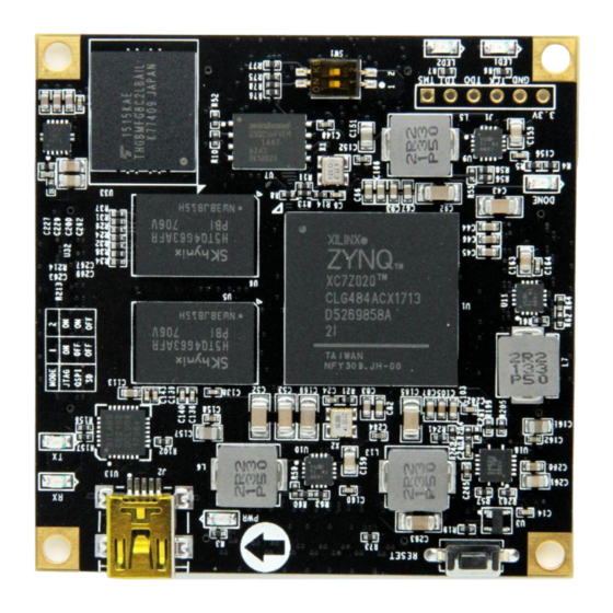
Part 1: AC7021 Core Board 1.1 Introduction The AC7021 (core board model, the same below) core board is an FPGA development board based on the Zynq chip XC7Z020-2CLG484I of the XILINX ZYNQ7000 series. The ZYNQ chip's PS system integrates two ARM CortexTM- A9 processors, AMBA®... - Page 5 ZYNQ FPGA Development Board AX7021 User Manual Figure 2-2-1: AC7021Core board Front View Amazon Store: https://www.amazon.com/alinx 5 / 30...
-
Page 6: Zyqn Chip
ZYNQ FPGA Development Board AX7021 User Manual Figure 2-2-2:AC7021 core board rear view 1.2 ZYQN Chip The development board uses Xilinx's Zynq7000 series chip, model XC7Z020-2CLG484I. The chip's PS system integrates two ARM CortexTM-A9 processors, AMBA® interconnects, internal memory, external memory interfaces and peripherals. - Page 7 Two SD card, SDIO, MMC compatible controllers 2 SPIs, 2 UARTs, 2 I2C interfaces 4 groups of 32bit GPIO, 54 (32+22) as PS system IO, 64 connected to High bandwidth connection within PS and PS to PL Amazon Store: https://www.amazon.com/alinx 7 / 30...
- Page 8 XC7Z020-2CLG484I chip speed grade is -2, industrial grade, package is BGA484, pin pitch is 0.024 inch, the specific chip model definition of ZYNQ7000 series is shown in Figure 2-2-4 Figure 2-2-4: The Specific Chip Model Definition of ZYNQ7000 Series Amazon Store: https://www.amazon.com/alinx 8 / 30...
-
Page 9: Ddr3 Dram
Figure 2-2-5: TheXC7Z020 chip used on the Core Board 1.3 DDR3 DRAM The AC7021 core board is equipped with two SK Hynix DDR3 SDRAM chips (1GB total), model H5TQ4G63AFR-PBI. The bus width of DDR3 SDRAM is 32 bits in total. DDR3 SDRAM has a maximum operating speed of 533MHz (data rate 1066Mbps). - Page 10 ZYNQ FPGA Development Board AX7021 User Manual The hardware connection of DDR3 DRAM is shown in Figure 2-3-1: Figure 2-3-1: The Schematic part of DDR3 DRAM Figure 2-3-2: DDR3 DRAM on the Core Board Amazon Store: https://www.amazon.com/alinx 10 / 30...
- Page 11 DDR3_D28 PS_DDR_DQ28_502 DDR3_D29 PS_DDR_DQ29_502 DDR3_D30 PS_DDR_DQ30_502 DDR3_D31 PS_DDR_DQ31_502 DDR3_DM0 PS_DDR_DM0_502 DDR3_DM1 PS_DDR_DM1_502 DDR3_DM2 PS_DDR_DM2_502 DDR3_DM3 PS_DDR_DM3_502 DDR3_A0 PS_DDR_A0_502 DDR3_A1 PS_DDR_A1_502 DDR3_A2 PS_DDR_A2_502 DDR3_A3 PS_DDR_A3_502 DDR3_A4 PS_DDR_A4_502 DDR3_A5 PS_DDR_A5_502 DDR3_A6 PS_DDR_A6_502 DDR3_A7 PS_DDR_A7_502 DDR3_A8 PS_DDR_A8_502 Amazon Store: https://www.amazon.com/alinx 11 / 30...
-
Page 12: Qspi Flash
ZYNQ chip. In the system design, the GPIO port functions of these PS ports need to be configured as the QSPI FLASH interface. Figure 2-4- 1 shows the QSPI Flash in the schematic. Amazon Store: https://www.amazon.com/alinx 12 / 30... -
Page 13: Emmc Flash
THGBMFG8C2LBAIL, which supports the JEDEC e-MMC V5.0 standard HS-MMC interface with level support of 1.8V or 3.3V. The data width of the eMMC FLASH and ZYNQ connections is 4 bits. Due to the large capacity and Amazon Store: https://www.amazon.com/alinx 13 / 30... - Page 14 PS ports need to be configured as the SD interface. Figure 2-5-1 shows the eMMC Flash in the schematic. Figure 2-5-1: eMMC Flash in the Schematic Figure 2-5-2: eMMC Flash on the Core Board Amazon Store: https://www.amazon.com/alinx 14 / 30...
-
Page 15: Clock Configuration
PS_MIO51_501 Table 2-5-2: Pin Assignment of eMMC FLASH 1.6 Clock configuration The AC7021 core board provides active clocks for the PS system and the PL logic sections, respectively, so that the PS system and the PL logic can work independently. -
Page 16: Usb To Serial Port
Table 2-6-2: PL Clock pin assignment 1.7 USB to serial port For the AC7021 core board to work and debug separately, we have a Uart to USB interface for the core board. Used for separate power supply and debugging of the core board. The conversion chip uses the USB-UART chip of Silicon Labs CP2102GM. - Page 17 LEDs on the PCB are printed as RX and TX LEDs (D5 and D6). The RX and TX LEDs indicate whether the serial port has data received or sent, as shown in the Figure 2-7-3 below. Figure 2-7-3: USB to serial port signal indicator Amazon Store: https://www.amazon.com/alinx 17 / 30...
-
Page 18: Led
Table 2-7-1: Uart Pin Assignment 1.8 LED There are 6 red LED lights on the AC7021 core board, one of which is the power indicator light (PWR), one is the configuration LED light (DONE), two are the user LED lights (LED1~LED2), and the other two are the UART transmit and receive indicators (TX, RX). -
Page 19: Reset Button
Table 2-8-1: LED Pin Assignment 1.9 Reset button The AC7021 has a reset button RESET and circuitry on the core board. The reset signal is connected to the PS reset pin of the ZYNQ chip. The reset button can be used by the user to reset the ZYNQ system. When the reset button is pressed, the reset chip will generate a low level reset signal to the ZYNQ chip. -
Page 20: Jtage Interface
Table 2-9-1: Reset Pin Assignment 1.10 JTAGE Interface The JTAG test socket J1 is reserved on the AC7021 core board for separate JTAG download and debugging of the core board. Figure 2-10-1 is the schematic part of the JTAG port, which involves TMS, TDI, TDO, TCK, GND. , +3.3V these six signals. -
Page 21: Dip Switch Configuration
Figure 2-10-2: JTAG interface on the core board 1.11 DIP switch configuration The AC7021 has a 2-digit DIP switch SW1 on the core board to configure the ZYNQ system's startup mode. The AC7021 system development platform supports three startup modes. The three startup modes are JTAG debug mode, QSPI FLASH and SD card boot mode. - Page 22 BANK33, 34 outputs a voltage standard of 2.5V. 1.5V generates the VTT and VREF voltages required by DDR3 through TI's TPS51200. The functions of each power distribution are shown in the following Table 2-12-1: Amazon Store: https://www.amazon.com/alinx 22 / 30...
- Page 23 +1.0V->+1.8V->(+1.5 V, +3.3V, VCCIO). The circuit design ensures the normal operation of the chip. The power supply on the core board detailed as Figure 2-12-2 below Figure 2-12-2: The Power Supply on the Core Board Amazon Store: https://www.amazon.com/alinx 23 / 30...
-
Page 24: Structure Diagram
The IO levels of BANK33 and BANK34 can be changed by changing the level of the LDO chip (U12) on the board. The default is 3.3V. Pin assignment detailed as Table 2-14-1, Table 2-14-2, Table 2-14-3, Table 2-14-4: Amazon Store: https://www.amazon.com/alinx 24 / 30... - Page 25 ZYNQ Pin ZYNQ Pin PS_MIO13 ETH_TXD0 PS_MIO12 ETH_TXD1 ETH_TXD2 ETH_TXD3 ETH_TXCK ETH_TXCTL ETH_RXD3 ETH_RXD2 PS_MIO7 ETH_RXD1 PS_MIO8 ETH_RXD0 PS_MIO9 ETH_RXCTL PS_MIO11 ETH_RXCK ETH_MDC ETH_MDIO OTG_STP OTG_DIR XADC_VP OTG_CLK XADC_VN OTG_NXT OTG_DATA0 PS_MIO10 OTG_DATA1 SD_CLK OTG_DATA2 Amazon Store: https://www.amazon.com/alinx 25 / 30...
- Page 26 B13_L1_N B33_L4_N B13_L1_P B33_L4_P B33_L10_P AB19 B33_L3_N B33_L10_N AB20 B33_L3_P B13_L4_N B33_L2_N B13_L4_P B33_L2_P B34_L6_N B13_L5_N B34_L6_P B13_L5_P B13_L12_N B33_IO25 B13_IO25 B34_IO25 B13_L23_N B13_L6_P B13_L23_P B13_L6_N B13_L13_N B13_L19_N B13_L13_P B13_L19_P B13_L24_N B13_L22_P B13_L24_P B13_L22_N Amazon Store: https://www.amazon.com/alinx 26 / 30...
- Page 27 B13_L17_P B13_L15_P B13_L21_N B13_L21_P Table 2-14-2: Pin Assignment of CON2 ZYNQ Pin ZYNQ Pin CON3 Pin Signal Name CON3 Pin Signal Name B34_L2_P B34_L12_N B34_L2_N B34_L12_P B34_L11_P B34_L10_N B34_L11_N B34_L10_P B34_L7_P B34_L3_N B34_L7_N B34_L3_P Amazon Store: https://www.amazon.com/alinx 27 / 30...
- Page 28 B33_L13_P B33_L17_N AB17 B33_L13_N B33_L17_P AA17 B33_L18_N AB16 B33_L7_P AA22 B33_L18_P AA16 B33_L7_N AB22 B33_L21_N B33_L19_N B33_L21_P B33_L19_P B33_L24_P AB14 B33_L15_N B33_L24_N AB15 B33_L15_P B33_L23_N AA13 B33_L14_P B33_L23_P B33_L14_N B33_L20_N B33_L22_P B33_L20_P B33_L22_N AA14 Amazon Store: https://www.amazon.com/alinx 28 / 30...
- Page 29 B35_L13_N B35_L18_N B35_L13_P B35_L18_P B35_L14_N B35_L16_N B35_L14_P B35_L16_P B35_L12_P B35_L17_N B35_L12_N B35_L17_P B35_L2_N B35_L23_N B35_L2_P B35_L23_P B35_L1_N B35_L22_N B35_L1_P B35_L22_P B35_L21_P B34_L8_N B35_L21_N B34_L8_P B35_L24_P B35_L20_N B35_L24_N B35_L20_P B35_L6_P B35_L19_N B35_L6_N B35_L19_P B35_L4_P B34_L9_P Amazon Store: https://www.amazon.com/alinx 29 / 30...
- Page 30 ZYNQ FPGA Development Board AX7021 User Manual B35_L4_N B34_L9_N B35_L3_N B35_IO25 B35_L3_P B35_IO0 B34_L24_N B34_L4_P B34_L24_P B34_L4_N B34_L23_P B34_L18_N B34_L23_N B34_L18_P B35_L5_P B34_L22_P B35_L5_N B34_L22_N B34_L19_P B34_L19_N Table 2-14-4: Pin Assignment of CON4 Amazon Store: https://www.amazon.com/alinx 30 / 30...
Need help?
Do you have a question about the AC7021 and is the answer not in the manual?
Questions and answers