Alinx ZYNQ7000 FPGA AC7021B User Manual
Hide thumbs
Also See for ZYNQ7000 FPGA AC7021B:
- User manual (61 pages) ,
- User manual (53 pages) ,
- User manual (48 pages)
Table of Contents
Advertisement
Quick Links
Advertisement
Table of Contents

Related Manuals for Alinx ZYNQ7000 FPGA AC7021B


Summary of Contents for Alinx ZYNQ7000 FPGA AC7021B
- Page 1 ZYNQ7000 FPGA Development Board AC7021BB System on Module...
- Page 2 ZYNQ FPGA Development Board AC7021B User Manual Version Record Version Date Release By Description Rev 1.0 2020-06-29 Rachel Zhou First Release 2 / 57 Amazon Store: https://www.amazon.com/alinx...
-
Page 3: Table Of Contents
Part 7: USB to serial port Part 8: LED Part 9: Reset button Part 10: JTAGE Interface Part 11: DIP switch configuration Part 12: Power Part 13 Structure diagram: Part 14: Connector pin definition 3 / 57 Amazon Store: https://www.amazon.com/alinx... -
Page 4: Part 1: Ac7021B Core Board Introduction
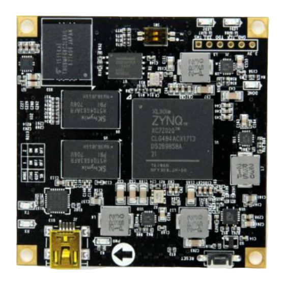
Moreover, the IOs connection part, the routing between the ZYNQ FPGA chip and the interface is equal length and differential processing. The core board size is only 2.36 inch* 2.36 inch, which is very suitable for secondary development. 4 / 30 Amazon Store: https://www.amazon.com/alinx... - Page 5 ZYNQ FPGA Development Board AC7021B User Manual Figure 1-1: AC7021BCore board Front View Figure 1-2:AC7021B core board rear view 5 / 30 Amazon Store: https://www.amazon.com/alinx...
-
Page 6: Part 2: Zyqn Chip
32KB level 1 instruction and data cache per CPU, 512KB level 2 cache 2 CPU shares On-chip boot ROM and 256KB on-chip RAM External storage interface, support 16/32 bit DDR2, DDR3 interface Two Gigabit NIC support: divergent-aggregate DMA, GMII, RGMII, 6 / 30 Amazon Store: https://www.amazon.com/alinx... - Page 7 XC7Z020-2CLG484I chip speed grade is -2, industrial grade, package is BGA484, pin pitch is 0.024 inch, the specific chip model definition of ZYNQ7000 series is shown in Figure 2-2 Figure 2-2: The Specific Chip Model Definition of ZYNQ7000 Series 7 / 30 Amazon Store: https://www.amazon.com/alinx...
-
Page 8: Part 3 Ddr3 Dram
The hardware design of DDR3 requires strict consideration of signal integrity. We have fully considered the matching resistor/terminal resistance, trace impedance control, and trace length control in circuit design and PCB design to ensure high-speed and stable operation of DDR3. 8 / 30 Amazon Store: https://www.amazon.com/alinx... - Page 9 ZYNQ FPGA Development Board AC7021B User Manual The hardware connection of DDR3 DRAM is shown in Figure 3-1: Figure 3-1: The Schematic part of DDR3 DRAM Figure 3-2: DDR3 DRAM on the Core Board 9 / 30 Amazon Store: https://www.amazon.com/alinx...
- Page 10 PS_DDR_DQ28_502 DDR3_D28 PS_DDR_DQ29_502 DDR3_D29 PS_DDR_DQ30_502 DDR3_D30 PS_DDR_DQ31_502 DDR3_D31 PS_DDR_DM0_502 DDR3_DM0 PS_DDR_DM1_502 DDR3_DM1 PS_DDR_DM2_502 DDR3_DM2 PS_DDR_DM3_502 DDR3_DM3 PS_DDR_A0_502 DDR3_A0 PS_DDR_A1_502 DDR3_A1 PS_DDR_A2_502 DDR3_A2 PS_DDR_A3_502 DDR3_A3 PS_DDR_A4_502 DDR3_A4 PS_DDR_A5_502 DDR3_A5 PS_DDR_A6_502 DDR3_A6 PS_DDR_A7_502 DDR3_A7 PS_DDR_A8_502 DDR3_A8 10 / 30 Amazon Store: https://www.amazon.com/alinx...
-
Page 11: Part 4 Qspi Flash
ZYNQ chip. In the system design, the GPIO port functions of these PS ports need to be configured as the QSPI FLASH interface. Figure 4-1 shows the QSPI Flash in the schematic. 11 / 30 Amazon Store: https://www.amazon.com/alinx... -
Page 12: Part 5: Emmc Flash
The core board is equipped with a large capacity 32GB eMMC FLASH chip, model THGBMFG8C2LBAIL, which supports the JEDEC e-MMC V5.0 standard HS-MMC interface with level support of 1.8V or 3.3V. The data width of the 12 / 30 Amazon Store: https://www.amazon.com/alinx... - Page 13 PS ports need to be configured as the SD interface. Figure 5-1 shows the eMMC Flash in the schematic. MMC_CCLK MMC_CMD eMMC ZYNQ BANK (THGBMFG8C2 LBAIL) MMC_DAT0~MMC_DAT3 Figure 5-1: eMMC Flash in the Schematic 13 / 30 Amazon Store: https://www.amazon.com/alinx...
-
Page 14: Part 6: Clock Configuration
X1 crystal on the development board. The input of the clock is connected to the pins of PS_CLK_500 of the BANK500 of the ZYNQ chip. The schematic diagram is shown in Figure 6-1: 14 / 30 Amazon Store: https://www.amazon.com/alinx... - Page 15 (MRCC) of the FPGA BANK13, which can be used to drive user logic within the FPGA. The schematic diagram of the clock source is shown in Figure 6-3: Figure 6-3: PL system clock source 15 / 30 Amazon Store: https://www.amazon.com/alinx...
-
Page 16: Part 7: Usb To Serial Port
USB port of the upper PC with a USB cable for separate power supply and serial data communication of the core board. UART_TXD VBUS BANK ZYNQ UART-USB REGIN UART_RXD (CP2102-GM) D+/- Micro USB Figure 7-1: USB to Serial Port 16 / 30 Amazon Store: https://www.amazon.com/alinx... -
Page 17: Part8: Led
Table 7-1: Uart Pin Assignment Part8: LED There are 6 red LED lights on the AC7021B core board, one of which is the power indicator light (PWR), one is the configuration LED light (DONE), two are 17 / 30 Amazon Store: https://www.amazon.com/alinx... - Page 18 The schematic diagram of the LED light hardware connection is shown in Figure 8-1: 3.3V 3.3V 3.3V LED1 LED2 BANK ZYNQ BANK 3.3V BANK DONE Figure 8-1: The schematic diagram of the LED light hardware connection 18 / 30 Amazon Store: https://www.amazon.com/alinx...
-
Page 19: Part 9: Reset Button
ZYNQ system. When the reset button is pressed, the reset chip will generate a low level reset signal to the ZYNQ chip. The schematic diagram of the reset button and reset chip connection is shown in Figure 9-1: 19 / 30 Amazon Store: https://www.amazon.com/alinx... -
Page 20: Part 10: Jtage Interface
JTAG download and debugging of the core board. Figure 10-1 is the schematic part of the JTAG port, which involves TMS, TDI, TDO, TCK, GND. , +3.3V these six signals. Figure 10-1: JTAG interface part of the core board schematic 20 / 30 Amazon Store: https://www.amazon.com/alinx... -
Page 21: Part 11: Dip Switch Configuration
The AC7021B core board is powered by DC5V. It is powered by the Mini USB interface when it is used alone. It is powered by the extension board when the backplane is connected. Please be careful not to supply power to the Mini 21 / 30 Amazon Store: https://www.amazon.com/alinx... - Page 22 BANK33, 34 outputs a voltage standard of 2.5V. 1.5V generates the VTT and VREF voltages required by DDR3 through TI's TPS51200. The functions of each power distribution are shown in the following Table 12-1: 22 / 30 Amazon Store: https://www.amazon.com/alinx...
- Page 23 +1.0V->+1.8V->(+1.5 V, +3.3V, VCCIO). The circuit design ensures the normal operation of the chip. The power supply on the core board detailed as Figure 12-2 below Figure 12-2: The Power Supply on the Core Board 23 / 30 Amazon Store: https://www.amazon.com/alinx...
-
Page 24: Part 13 Structure Diagram
The IO levels of BANK33 and BANK34 can be changed by changing the level of the LDO chip (U12) on the board. The default is 3.3V. Pin assignment detailed as Table 14-1, Table 14-2, Table 14-3, Table 14-4: 24 / 30 Amazon Store: https://www.amazon.com/alinx... - Page 25 ZYNQ Pin ZYNQ Pin PS_MIO13 ETH_TXD0 PS_MIO12 ETH_TXD1 ETH_TXD2 ETH_TXD3 ETH_TXCK ETH_TXCTL ETH_RXD3 ETH_RXD2 PS_MIO7 ETH_RXD1 PS_MIO8 ETH_RXD0 PS_MIO9 ETH_RXCTL PS_MIO11 ETH_RXCK ETH_MDC ETH_MDIO OTG_STP OTG_DIR XADC_VP OTG_CLK XADC_VN OTG_NXT OTG_DATA0 PS_MIO10 OTG_DATA1 SD_CLK OTG_DATA2 25 / 30 Amazon Store: https://www.amazon.com/alinx...
- Page 26 B13_L1_N B33_L4_N B13_L1_P B33_L4_P B33_L10_P AB19 B33_L3_N B33_L10_N AB20 B33_L3_P B13_L4_N B33_L2_N B13_L4_P B33_L2_P B34_L6_N B13_L5_N B34_L6_P B13_L5_P B13_L12_N B33_IO25 B13_IO25 B34_IO25 B13_L23_N B13_L6_P B13_L23_P B13_L6_N B13_L13_N B13_L19_N B13_L13_P B13_L19_P B13_L24_N B13_L22_P B13_L24_P B13_L22_N 26 / 30 Amazon Store: https://www.amazon.com/alinx...
- Page 27 B13_L17_P B13_L15_P B13_L21_N B13_L21_P Table 14-2: Pin Assignment of CON2 ZYNQ Pin ZYNQ Pin CON3 Pin Signal Name CON3 Pin Signal Name B34_L2_P B34_L12_N B34_L2_N B34_L12_P B34_L11_P B34_L10_N B34_L11_N B34_L10_P B34_L7_P B34_L3_N B34_L7_N B34_L3_P 27 / 30 Amazon Store: https://www.amazon.com/alinx...
- Page 28 B33_L13_P B33_L17_N AB17 B33_L13_N B33_L17_P AA17 B33_L18_N AB16 B33_L7_P AA22 B33_L18_P AA16 B33_L7_N AB22 B33_L21_N B33_L19_N B33_L21_P B33_L19_P B33_L24_P AB14 B33_L15_N B33_L24_N AB15 B33_L15_P B33_L23_N AA13 B33_L14_P B33_L23_P B33_L14_N B33_L20_N B33_L22_P B33_L20_P B33_L22_N AA14 28 / 30 Amazon Store: https://www.amazon.com/alinx...
- Page 29 B35_L13_N B35_L18_N B35_L13_P B35_L18_P B35_L14_N B35_L16_N B35_L14_P B35_L16_P B35_L12_P B35_L17_N B35_L12_N B35_L17_P B35_L2_N B35_L23_N B35_L2_P B35_L23_P B35_L1_N B35_L22_N B35_L1_P B35_L22_P B35_L21_P B34_L8_N B35_L21_N B34_L8_P B35_L24_P B35_L20_N B35_L24_N B35_L20_P B35_L6_P B35_L19_N B35_L6_N B35_L19_P B35_L4_P B34_L9_P 29 / 30 Amazon Store: https://www.amazon.com/alinx...
- Page 30 ZYNQ FPGA Development Board AC7021B User Manual B35_L4_N B34_L9_N B35_L3_N B35_IO25 B35_L3_P B35_IO0 B34_L24_N B34_L4_P B34_L24_P B34_L4_N B34_L23_P B34_L18_N B34_L23_N B34_L18_P B35_L5_P B34_L22_P B35_L5_N B34_L22_N B34_L19_P B34_L19_N Table 14-4: Pin Assignment of CON4 30 / 30 Amazon Store: https://www.amazon.com/alinx...
Need help?
Do you have a question about the ZYNQ7000 FPGA AC7021B and is the answer not in the manual?
Questions and answers