Table of Contents
Advertisement
Quick Links
Advertisement
Table of Contents

Related Manuals for Alinx ACU7EVB


Summary of Contents for Alinx ACU7EVB
- Page 1 ZYNQ UltraScale+ FPGA Core Board ACU7EVB User Manual...
-
Page 2: Version Record
ZYNQ Ultrascale + FPGA Core Board ACU7EVB User Manual Version Record Version Date Description Rev 1.0 2022-08-30 First Release Amazon Store: https://www.amazon.com/alinx 2 / 31... -
Page 3: Table Of Contents
ZYNQ Ultrascale + FPGA Core Board ACU7EVB User Manual CONTENTS Version Record .....................2 Part 1: ACU7EVB Core Board ..............4 Part 1.1: ACU7EVB Core Board Introduction ..........4 Part 1.2: ZYNQ Chip ..................5 Part 1.3: DDR4 DRAM ................. 7 Part 1.4: QSPI Flash .................. 16 Part 1.5: eMMC Flash ................ -
Page 4: Part 1: Acu7Evb Core Board
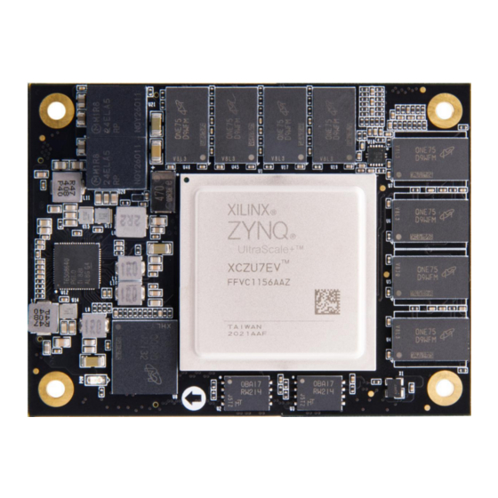
ZYNQ Ultrascale + FPGA Core Board ACU7EVB User Manual Part 1: ACU7EVB Core Board Part 1.1: ACU7EVB Core Board Introduction ACU7EVB (core board model, the same below) FPGA core board, ZYNQ chip is based on XCZU7EV-2FFVB1156I of XILINX company Zynq UltraScale+ MPSoCs EG Family. -
Page 5: Part 1.2: Zynq Chip
Figure 2-1-1: ACU7EVB Core Board (Front View) Part 1.2: ZYNQ Chip The FPGA core board ACU7EVB uses Xilinx's Zynq UltraScale+ MPSoCs EV family chip, module XCZU7EV-2FFVB1156I. The PS system of the ZU7EV chip integrates 4 ARM Cortex™-A53 processors with a speed of up to 1.3Ghz and supports Level 2 Cache;... - Page 6 ZYNQ Ultrascale + FPGA Core Board ACU7EVB User Manual Figure 2-2-1: Overall Block Diagram of the ZYNQ ZU7EV Chip The main parameters of the PS system part are as follows: ARM quad-core Cortex ™ -A53 processor, speed up to 1.3GHz, each...
-
Page 7: Part 1.3: Ddr4 Dram
DSP Slices: 1728 Part 1.3: DDR4 DRAM The ACU7EVB core board is equipped with 8 Micron (Micron) 1GB DDR4 chips, model MT40A512M16LY-062E, of which 4 DDR4 chips are mounted on the PS side to form a 64-bit data bus bandwidth and 4GB capacity. Four DDR4 chip is mounted on the PL end, which is a 64-bit data bus width and a capacity of 4GB. - Page 8 ZYNQ Ultrascale + FPGA Core Board ACU7EVB User Manual BANK66,67,68 interface of the FPGA. The specific configuration of DDR4 SDRAM is shown in Table 2-3-1 below: Position Bit Number Chip Model Capacity Factory U4,U5,U6,U7 MT40A512M16LY-062E 512M x 16bit Micron U17,U19,U45,U46...
- Page 9 ZYNQ Ultrascale + FPGA Core Board ACU7EVB User Manual Figure 2-3-2: DDR4 DRAM schematic diagram PS Side DDR4 DRAM pin assignment: Signal Name Pin Name Pin Number PS_DDR4_DQS0_N PS_DDR_DQS_N0_504 AN27 PS_DDR4_DQS0_P PS_DDR_DQS_P0_504 AN26 PS_DDR4_DQS1_N PS_DDR_DQS_N1_504 AP30 PS_DDR4_DQS1_P PS_DDR_DQS_P1_504 AN29 PS_DDR4_DQS2_N...
- Page 10 ZYNQ Ultrascale + FPGA Core Board ACU7EVB User Manual PS_DDR4_DQ0 PS_DDR_DQ0_504 AP27 PS_DDR4_DQ1 PS_DDR_DQ1_504 AP25 PS_DDR4_DQ2 PS_DDR_DQ2_504 AP26 PS_DDR4_DQ3 PS_DDR_DQ3_504 AM26 PS_DDR4_DQ4 PS_DDR_DQ4_504 AP24 PS_DDR4_DQ5 PS_DDR_DQ5_504 AL25 PS_DDR4_DQ6 PS_DDR_DQ6_504 AM25 PS_DDR4_DQ7 PS_DDR_DQ7_504 AM24 PS_DDR4_DQ8 PS_DDR_DQ8_504 AM28 PS_DDR4_DQ9 PS_DDR_DQ9_504 AN28 PS_DDR4_DQ10...
- Page 11 ZYNQ Ultrascale + FPGA Core Board ACU7EVB User Manual PS_DDR4_DQ36 PS_DDR_DQ36_504 AC31 PS_DDR4_DQ37 PS_DDR_DQ37_504 AE30 PS_DDR4_DQ38 PS_DDR_DQ38_504 AC28 PS_DDR4_DQ39 PS_DDR_DQ39_504 AE29 PS_DDR4_DQ40 PS_DDR_DQ40_504 AC27 PS_DDR4_DQ41 PS_DDR_DQ41_504 AA27 PS_DDR4_DQ42 PS_DDR_DQ42_504 AA28 PS_DDR4_DQ43 PS_DDR_DQ43_504 AB28 PS_DDR4_DQ44 PS_DDR_DQ44_504 PS_DDR4_DQ45 PS_DDR_DQ45_504 PS_DDR4_DQ46 PS_DDR_DQ46_504 PS_DDR4_DQ47...
- Page 12 ZYNQ Ultrascale + FPGA Core Board ACU7EVB User Manual PS_DDR4_A0 PS_DDR_A0_504 AN34 PS_DDR4_A1 PS_DDR_A1_504 AM34 PS_DDR4_A2 PS_DDR_A2_504 AM33 PS_DDR4_A3 PS_DDR_A3_504 AL34 PS_DDR4_A4 PS_DDR_A4_504 AL33 PS_DDR4_A5 PS_DDR_A5_504 AK33 PS_DDR4_A6 PS_DDR_A6_504 AK30 PS_DDR4_A7 PS_DDR_A7_504 AJ30 PS_DDR4_A8 PS_DDR_A8_504 AJ31 PS_DDR4_A9 PS_DDR_A9_504 AH31 PS_DDR4_A10...
- Page 13 ZYNQ Ultrascale + FPGA Core Board ACU7EVB User Manual PL_DDR4_DQS1_P IO_L4P_T0U_N6_DBC_AD7P_67 PL_DDR4_DQS2_N IO_L16N_T2U_N7_QBC_AD3N_67 PL_DDR4_DQS2_P IO_L16P_T2U_N6_QBC_AD3P_67 PL_DDR4_DQS3_N IO_L22N_T3U_N7_DBC_AD0N_67 PL_DDR4_DQS3_P IO_L22P_T3U_N6_DBC_AD0P_67 PL_DDR4_DQS4_N IO_L16N_T2U_N7_QBC_AD3N_68 PL_DDR4_DQS4_P IO_L16P_T2U_N6_QBC_AD3P_68 PL_DDR4_DQS5_N IO_L22N_T3U_N7_DBC_AD0N_68 PL_DDR4_DQS5_P IO_L22P_T3U_N6_DBC_AD0P_68 PL_DDR4_DQS6_N IO_L10N_T1U_N7_QBC_AD4N_68 PL_DDR4_DQS6_P IO_L10P_T1U_N6_QBC_AD4P_68 PL_DDR4_DQS7_N IO_L4N_T0U_N7_DBC_AD7N_68 PL_DDR4_DQS7_P IO_L4P_T0U_N6_DBC_AD7P_68 PL_DDR4_DQ0 IO_L9N_T1L_N5_AD12N_67 PL_DDR4_DQ1 IO_L11P_T1U_N8_GC_67 PL_DDR4_DQ2...
- Page 14 ZYNQ Ultrascale + FPGA Core Board ACU7EVB User Manual PL_DDR4_DQ23 IO_L14P_T2L_N2_GC_67 PL_DDR4_DQ24 IO_L24N_T3U_N11_67 PL_DDR4_DQ25 IO_L21N_T3L_N5_AD8N_67 PL_DDR4_DQ26 IO_L23P_T3U_N8_67 PL_DDR4_DQ27 IO_L21P_T3L_N4_AD8P_67 PL_DDR4_DQ28 IO_L24P_T3U_N10_67 PL_DDR4_DQ29 IO_L20P_T3L_N2_AD1P_67 PL_DDR4_DQ30 IO_L23N_T3U_N9_67 PL_DDR4_DQ31 IO_L20N_T3L_N3_AD1N_67 PL_DDR4_DQ32 IO_L18N_T2U_N11_AD2N_68 PL_DDR4_DQ33 IO_L17P_T2U_N8_AD10P_68 PL_DDR4_DQ34 IO_L17N_T2U_N9_AD10N_68 PL_DDR4_DQ35 IO_L14P_T2L_N2_GC_68 PL_DDR4_DQ36 IO_L18P_T2U_N10_AD2P_68 PL_DDR4_DQ37 IO_L15N_T2L_N5_AD11N_68 PL_DDR4_DQ38...
- Page 15 ZYNQ Ultrascale + FPGA Core Board ACU7EVB User Manual PL_DDR4_DQ59 IO_L2P_T0L_N2_68 PL_DDR4_DQ60 IO_L6P_T0U_N10_AD6P_68 PL_DDR4_DQ61 IO_L3P_T0L_N4_AD15P_68 PL_DDR4_DQ62 IO_L2N_T0L_N3_68 PL_DDR4_DQ63 IO_L3N_T0L_N5_AD15N_68 PL_DDR4_DM0 IO_L7P_T1L_N0_QBC_AD13P_67 PL_DDR4_DM1 IO_L1P_T0L_N0_DBC_67 PL_DDR4_DM2 IO_L13P_T2L_N0_GC_QBC_67 PL_DDR4_DM3 IO_L19P_T3L_N0_DBC_AD9P_67 PL_DDR4_DM4 IO_L13P_T2L_N0_GC_QBC_68 PL_DDR4_DM5 IO_L19P_T3L_N0_DBC_AD9P_68 PL_DDR4_DM6 IO_L7P_T1L_N0_QBC_AD13P_68 PL_DDR4_DM7 IO_L1P_T0L_N0_DBC_68 PL_DDR4_A0 IO_L10P_T1U_N6_QBC_AD4P_66 PL_DDR4_A1 IO_L6P_T0U_N10_AD6P_66 PL_DDR4_A2...
-
Page 16: Part 1.4: Qspi Flash
IO_L13P_T2L_N0_GC_QBC_66 AH12 Part 1.4: QSPI Flash The FPGA core board ACU7EVB is equipped with two 256MBit Quad-SPI FLASH chip to form an 8-bit bandwidth data bus, the flash model is MT25QU256ABA1EW9, which uses the 1.8V CMOS voltage standard. Due to the non-volatile nature of QSPI FLASH, it can be used as a boot device for the system to store the boot image of the system. -
Page 17: Part 1.5: Emmc Flash
PS_MIO2_500 MIO3_QSPI0_IO3 PS_MIO3_500 MIO4_QSPI0_IO0 PS_MIO4_500 MIO5_QSPI0_SS_B PS_MIO5_500 MIO10_QSPI1_IO2 PS_MIO10_500 MIO11_QSPI1_IO3 PS_MIO11_500 MIO12_QSPI1_SCLK PS_MIO12_500 MIO7_QSPI1_SS_B PS_MIO7_500 MIO8_QSPI1_IO0 PS_MIO8_500 MIO9_QSPI1_IO1 PS_MIO9_500 Part 1.5: eMMC Flash The ACU7EVB core board is equipped with a large-capacity 8GB eMMC Amazon Store: https://www.amazon.com/alinx 17 / 31... - Page 18 ZYNQ Ultrascale + FPGA Core Board ACU7EVB User Manual FLASH chip, the model is MTFC8GAKAJCN-4M, it supports the HS-MMC interface of the JEDEC e-MMC V5.0 standard, and the level supports 1.8V or 3.3V. The data width of eMMC FLASH and ZYNQ connection is 8bit. Due to the...
-
Page 19: Part 1.6: Clock Configuration
Figure 2-6-1: Core Board Clock Source Part 1.7: Power Supply The power supply voltage of the ACU7EVB core board is DC12V, which is supplied by connecting the carrier board. The core board uses 2 MYMGM1R824 power chips in parallel to achieve a 50A current to provide the Amazon Store: https://www.amazon.com/alinx... - Page 20 ZYNQ Ultrascale + FPGA Core Board ACU7EVB User Manual core power of the XCZU7EV with 0.85V. In addition, a PMIC chip TPS6508640 is used to generate all other power supplies required by the XCZU7EV chip. For the TPS6508640 power supply design, please refer to the power supply chip manual.
-
Page 21: Part 1.8: Acu7Evb Core Board Size Dimension
ZYNQ Ultrascale + FPGA Core Board ACU7EVB User Manual The BANK28, BANK64, and BANK65 levels of the XCZU7EV chip are powered by the LDO alone, which can change the voltage by replacing the LDO chip (up to 1.8V support). Part 1.8: ACU7EVB Core Board Size Dimension Figure 2-8-1: ACU7EVB Core Board Size Dimension Part 1.9: Board to Board Connectors pin assignment... - Page 22 ZYNQ Ultrascale + FPGA Core Board ACU7EVB User Manual AXK6A2337YG. J29 connector J29 connects to +12V power supply, the IO of BANK28, BANK87,BANK88. the level standard of BANK87, 88 is 3.3V, the level standard of BANK28 is 1.8V, The Level of PS MIO is +1.8V.
- Page 23 ZYNQ Ultrascale + FPGA Core Board ACU7EVB User Manual B87_L11_N B87_L3_N B87_L11_P B87_L3_P B87_L5_N B87_L12_N B87_L5_P B87_L12_P B87_L8_N B87_L7_N B87_L8_P B87_L7_P B87_L2_N B87_L6_N B87_L2_P B87_L6_P B87_L4_N B28_L7_N B87_L4_P B28_L7_P B28_L20_N B28_L9_N B28_L20_P B28_L9_P B28_L19_N B28_L10_N B28_L19_P B28_L10_P B28_L21_N B28_L22_N B28_L21_P...
- Page 24 ZYNQ Ultrascale + FPGA Core Board ACU7EVB User Manual PS_MIO28 PS_MIO38 Pin assignment of board to board connector J30 J30 connects the transceiver signal of bank505 Mgt, Mio of part PS and bank28. The default level standard of bank28 is 1.8V. The Mio level of PS is 1.8V standard.
- Page 25 ZYNQ Ultrascale + FPGA Core Board ACU7EVB User Manual PHY1_TXD0 PHY1_TXD1 PHY1_TXD2 PHY1_TXD3 PS_POR_B PHY1_TXCK FPGA_DONE PHY1_TXCTL PS_MODE3 PHY1_RXD3 PS_MODE2 PHY1_RXD2 PS_MODE1 PHY1_RXD1 PS_MODE0 PHY1_RXD0 FPGA_TCK PHY1_RXCTL FPGA_TDI PHY1_RXCK FPGA_TMS PHY1_MDC FPGA_TDO PHY1_MDIO 505_RX3_N 505_TX3_N 505_RX3_P 505_TX3_P 505_RX2_N 505_TX2_N 505_RX2_P...
- Page 26 ZYNQ Ultrascale + FPGA Core Board ACU7EVB User Manual 505_CLK2_P 505_CLK3_P Pin assignment of board to board connector J31 J31 connects the IO of BANK64, BANK65, the level standard of BANK66, 67 is +1.8V. J31 Pin Signal Name Pin Number...
- Page 27 ZYNQ Ultrascale + FPGA Core Board ACU7EVB User Manual B65_L22_N AB18 B65_L9_N AK19 B65_L22_P AA18 B65_L9_P AJ19 B64_L1_P AP18 B64_L9_P AK18 B64_L1_N AP17 B64_L9_N AL18 B64_L6_P AN17 B64_L14_P AF18 B64_L6_N AN16 B64_L14_N AG18 B64_L5_P AP16 B64_L11_P AJ17 B64_L5_N AP15 B64_L11_N...
- Page 28 ZYNQ Ultrascale + FPGA Core Board ACU7EVB User Manual J32 Pin Signal Name Pin Number J32 Pin Signal Name Pin Number 223_RX0_P 223_TX0_P 223_RX0_N 223_TX0_N 223_RX1_P 223_TX1_P 223_RX1_N 223_TX1_N 223_RX2_P 223_TX2_P 223_RX2_N 223_TX2_N 223_RX3_P 223_TX3_P 223_RX3_N 223_TX3_N 223_CLK1_P AC10 223_CLK0_P...
- Page 29 ZYNQ Ultrascale + FPGA Core Board ACU7EVB User Manual 225_TX1_P 225_TX0_P 225_TX1_N 225_TX0_N 225_RX2_P 225_RX3_P 225_RX2_N 225_RX3_N 225_TX2_P 225_TX3_P 225_TX2_N 225_TX3_N 226_CLK0_P 226_CLK1_P 226_CLK0_N 226_CLK1_N 226_RX3_P 226_TX3_P 226_RX3_N 226_TX3_N 226_RX2_P 226_TX2_P 226_RX2_N 226_TX2_N 226_RX1_P 226_TX1_P 226_RX1_N 226_TX1_N 226_RX0_P 226_TX0_P 226_RX0_N 226_TX0_N ...
- Page 30 ZYNQ Ultrascale + FPGA Core Board ACU7EVB User Manual clock source for the PS system. The crystal is connected to the PS_PADI_503 and PS_PADO_503 pins of BANK503 of the ZYNQ chip. The schematic diagram is shown in Figure 2-6-2: Figure 2-6-2: Passive Crystal Oscillator for RTC...
- Page 31 ZYNQ Ultrascale + FPGA Core Board ACU7EVB User Manual PS_REF_CLK PL System Clock Source The core board provides a differential 200MHz PL system clock source for the reference clock of the DDR4 controller. The crystal oscillator output is connected to the global clock (MRCC) of PL BANK64. This global clock can be used to drive the DDR4 controller and user logic circuits in the FPGA.
Need help?
Do you have a question about the ACU7EVB and is the answer not in the manual?
Questions and answers