Table of Contents
Advertisement
Advertisement
Table of Contents

Related Manuals for Alinx AC7Z100


Summary of Contents for Alinx AC7Z100
- Page 1 ZYNQ7000 FPGA Development Board AC7Z100 System on Module...
-
Page 2: Version Record
ZYNQ FPGA Development Board AC7Z100 User Manual Version Record Version Date Release By Description Rev 1.0 2020-06-28 Rachel Zhou First Release Amazon Store: https://www.amazon.com/alinx 2 / 33... -
Page 3: Table Of Contents
Part 7: LED Light ..................20 Part 8: Reset circuit ................21 Part 9: Power Supply ................22 Part 10: AC7Z100 Core Board Size Dimension ........24 Part 11: Board to Board Connectors Pin Assignment......25 Amazon Store: https://www.amazon.com/alinx 3 / 33... -
Page 4: Part 1: Ac7Z100 Core Board Introduction
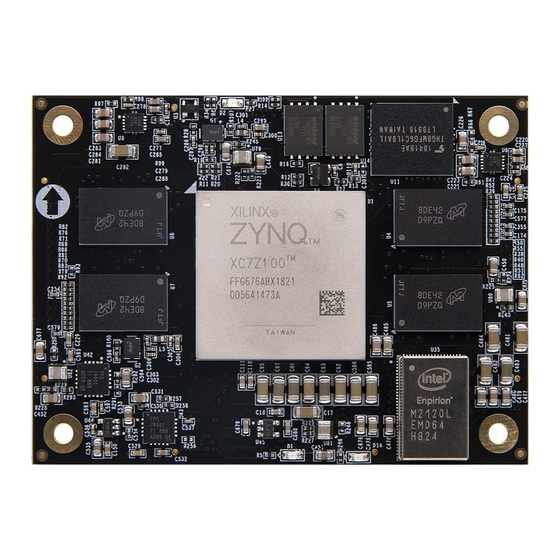
ZYNQ FPGA Development Board AC7Z100 User Manual Part 1: AC7Z100 Core Board Introduction AC7Z100 (core board model, the same below) FPGA core board, ZYNQ chip is based on XC7Z100-2FFG900 of XILINX company ZYNQ7000 series. The ZYNQ chip's PS system integrates two ARM CortexTM-A9 processors, AMBA®... -
Page 5: Part 2: Zynq Chip
ZYNQ FPGA Development Board AC7Z100 User Manual Figure 1-1: AC7Z100 Core Board (Front View) Figure 1-2: AC7Z100 Core Board (Rear View) Part 2: ZYNQ Chip The FPGA core board AC7Z100 uses Xilinx's Zynq7000 series chip, Amazon Store: https://www.amazon.com/alinx 5 / 33... - Page 6 ZYNQ FPGA Development Board AC7Z100 User Manual module XC7Z100-2FFG900. The chip's PS system integrates two ARM Cortex™-A9 processors, AMBA® interconnects, internal memory, external memory interfaces and peripherals. These peripherals mainly include USB bus interface, Ethernet interface, SD/SDIO interface, I2C bus interface, CAN bus interface, UART interface, GPIO etc.
- Page 7 ZYNQ FPGA Development Board AC7Z100 User Manual SGMII interface Two USB2.0 OTG interfaces, each supporting up to 12 nodes Two CAN2.0B bus interfaces Two SD card, SDIO, MMC compatible controllers 2 SPIs, 2 UARTs, 2 I2C interfaces ...
-
Page 8: Part 3: Ddr3 Dram
ZYNQ FPGA Development Board AC7Z100 User Manual Figure 2-2: The Specific Chip Model Definition of ZYNQ7000 Series Figure 2-3: The XC7Z100 chip used on the Core Board Part 3: DDR3 DRAM The FPGA core board AC7Z100 is equipped with four Micron 512MB DDR3 chips, model... - Page 9 ZYNQ FPGA Development Board AC7Z100 User Manual sides respectively. Two DDR3 SDRAMs form a 32-bit bus width. The PS-side DDR3 SDRAM has a maximum operating speed of 533MHz (data rate 1066Mbps), and two DDR3 memory systems are directly connected to the memory interface of the BANK 502 of the ZYNQ Processing System (PS).
- Page 10 ZYNQ FPGA Development Board AC7Z100 User Manual Figure 3-2: The Schematic Part of DDR3 DRAM on the PL side PS side DDR3 DRAM pin assignment: Signal Name ZYNQ Pin Name ZYNQ Pin Number PS_DDR_DQS_P0_502 PS_DDR3_DQS0_P PS_DDR_DQS_N0_502 PS_DDR3_DQS0_N PS_DDR_DQS_P1_502 PS_DDR3_DQS1_P PS_DDR_DQS_N1_502...
- Page 11 ZYNQ FPGA Development Board AC7Z100 User Manual PS_DDR_DQ9_502 PS_DDR3_D9 PS_DDR_DQ10_502 PS_DDR3_D10 PS_DDR_DQ11_502 PS_DDR3_D11 PS_DDR_DQ12_502 PS_DDR3_D12 PS_DDR_DQ13_502 PS_DDR3_D13 PS_DDR_DQ14_502 PS_DDR3_D14 PS_DDR_DQ15_502 PS_DDR3_D15 PS_DDR_DQ16_502 PS_DDR3_D16 PS_DDR_DQ17_502 PS_DDR3_D17 PS_DDR_DQ18_502 PS_DDR3_D18 PS_DDR_DQ19_502 PS_DDR3_D19 PS_DDR_DQ20_502 PS_DDR3_D20 PS_DDR_DQ21_502 PS_DDR3_D21 PS_DDR_DQ22_502 PS_DDR3_D22 PS_DDR_DQ23_502 PS_DDR3_D23 PS_DDR_DQ24_502 PS_DDR3_D24 PS_DDR_DQ25_502...
- Page 12 ZYNQ FPGA Development Board AC7Z100 User Manual PS_DDR_A6_502 PS_DDR3_A6 PS_DDR_A7_502 PS_DDR3_A7 PS_DDR_A8_502 PS_DDR3_A8 PS_DDR_A9_502 PS_DDR3_A9 PS_DDR_A10_502 PS_DDR3_A10 PS_DDR_A11_502 PS_DDR3_A11 PS_DDR_A12_502 PS_DDR3_A12 PS_DDR_A13_502 PS_DDR3_A13 PS_DDR_A14_502 PS_DDR3_A14 PS_DDR_BA0_502 PS_DDR3_BA0 PS_DDR_BA1_502 PS_DDR3_BA1 PS_DDR_BA2_502 PS_DDR3_BA2 PS_DDR_CS_B_502 PS_DDR3_S0 PS_DDR_RAS_B_502 PS_DDR3_RAS PS_DDR_CAS_B_502 PS_DDR3_CAS PS_DDR_WE_B_502 PS_DDR3_WE PS_DDR_ODT_502...
- Page 13 ZYNQ FPGA Development Board AC7Z100 User Manual IO_L1N_T0_33 PL_DDR3_D1 IO_L4P_T0_33 PL_DDR3_D2 IO_L1P_T0_33 PL_DDR3_D3 IO_L2N_T0_33 PL_DDR3_D4 IO_L5P_T0_33 PL_DDR3_D5 IO_L2P_T0_33 PL_DDR3_D6 IO_L4N_T0_33 PL_DDR3_D7 IO_L7N_T1_33 PL_DDR3_D8 IO_L10N_T1_33 PL_DDR3_D9 IO_L7P_T1_33 PL_DDR3_D10 IO_L8N_T1_33 PL_DDR3_D11 IO_L11N_T1_SRCC_33 PL_DDR3_D12 IO_L8P_T1_33 PL_DDR3_D13 IO_L11P_T1_SRCC_33 PL_DDR3_D14 IO_L10P_T1_33 PL_DDR3_D15 IO_L18P_T2_33 PL_DDR3_D16 IO_L14P_T2_SRCC_33...
-
Page 14: Part 4: Qspi Flash
IO_L21P_T3_DQS_34 PL_DDR3_CLK0_P IO_L21N_T3_DQS_34 PL_DDR3_CLK0_N IO_L24P_T3_34 PL_DDR3_CKE Part 4: QSPI Flash The FPGA core board AC7Z100 is equipped with two 256MBit Quad-SPI FLASH chips to form an 8-bit bandwidth data bus, the flash model is Amazon Store: https://www.amazon.com/alinx 14 / 33... - Page 15 ZYNQ FPGA Development Board AC7Z100 User Manual W25Q256FVEI, which uses the 3.3V CMOS voltage standard. Due to the non-volatile nature of QSPI FLASH, it can be used as a boot device for the system to store the boot image of the system. These images mainly include FPGA bit files, ARM application code, and other user data files.
-
Page 16: Part 5: Emmc Flash
PS_MIO13_500 QSPI1_D3 Part 5: eMMC Flash The FPGA core board AC7Z100 is equipped with a large-capacity 8GB eMMC FLASH chip, model THGBMFG6C1LBAIL, which supports the JEDEC e-MMC V5.0 standard HS-MMC interface with level support of 1.8V or 3.3V. The data width of the eMMC FLASH and ZYNQ connections is 4 bits. Due to... -
Page 17: Part 6: Clock Configuration
ZYNQ FPGA Development Board AC7Z100 User Manual MMC_CCLK MMC_CMD eMMC ZYNQ BANK (THGBMFG6C1 LBAIL) MMC_DAT0~MMC_DAT3 Figure 5-1: eMMC Flash in the Schematic Pin Assignment of eMMC Flash Signal Name ZYNQ Pin Name ZYNQ Pin Number PS_MIO48_501 MMC_CCLK PS_MIO47_501 MMC_CMD PS_MIO46_501... - Page 18 The ZYNQ chip provides a 33.333MHz clock input to the PS section via the X4 crystal on the FPGA core board AC7Z100. The input of the clock is connected to the pin of the PS_CLK_500 of the BANK500 of the ZYNQ chip.
- Page 19 PL system clock source The differential 200MHz PL system clock source is provided on the FPGA core board AC7Z100 for the reference clock of the DDR3 controller. The crystal output is connected to the global clock (MRCC) of the FPGA BANK34, which can be used to drive the DDR3 controller and user logic in the FPGA.
-
Page 20: Part 7: Led Light
BANK111_CLK1_N Part 7: LED Light There are 2 red LED lights on the AC7Z100 FPGA core board, one of which is the power indicator light (PWR), one is the configuration LED light (DONE). When the core board is powered, the power indicator will illuminate;... -
Page 21: Part 8: Reset Circuit
Figure 7-1: AC7Z100 FPGA Core board LED light Hardware Connection Part 8: Reset circuit There is a reset circuit on the AC7Z100 core board. The reset input signal is connected to the reset button on the carrier board. The reset output is connected to the PS reset pin of the ZYNQ chip. -
Page 22: Part 9: Power Supply
PS_POR_B_500 ZYNQ system reset signal Part 9: Power Supply The AC7Z100 FPGA core board is powered by DC5V and is powered by a connection carrier board. The power supply design diagram on the FPGA board is shown in Figure 9-1 Figure 9-1:Power interface section in the schematic... - Page 23 ZYNQ FPGA Development Board AC7Z100 User Manual supply generates +1.2V power required by GTX through the LDO chip TPS74401, and +3.3V generates GTX auxiliary power supply +1.8V through an LDO chip SPX3819-1-8. The VTT and VREF voltages of the DDR3 of the PS section and the PL section are generated by U7, U10.
-
Page 24: Part 10: Ac7Z100 Core Board Size Dimension
ZYNQ FPGA Development Board AC7Z100 User Manual Figure 9-2: Power Supply on the AX7Z100 Core Board Part 10: AC7Z100 Core Board Size Dimension Figure 10-1: AC7Z100 Core Board Size Dimension Amazon Store: https://www.amazon.com/alinx 24 / 33... -
Page 25: Part 11: Board To Board Connectors Pin Assignment
ZYNQ FPGA Development Board AC7Z100 User Manual Part Board Board Connectors Assignment The core board has a total of four high-speed expansion ports. It uses four 120-pin inter-board connectors (J29~J32) to connect to the carrier board. The connector uses the Panasonic AXK5A2147YG, and the connector type corresponding to the carrier board is AXK6A2337YG. - Page 26 ZYNQ FPGA Development Board AC7Z100 User Manual B11_L13_P AG21 B11_L17_P AH19 B11_L14_N AG20 B11_L18_N AG19 B11_L14_P AF20 B11_L18_P AF19 B11_L19_P AB21 B11_L20_N B11_L19_N AB22 B11_L20_P B10_L13_P AG17 B10_L17_P AE18 B10_L13_N AG16 B10_L17_N AE17 B10_L2_P AH18 B10_L15_P AF18 B10_L2_N AJ18 B10_L15_N...
- Page 27 ZYNQ FPGA Development Board AC7Z100 User Manual B10_L8_P AH14 B10_L3_P AJ14 B10_L8_N AH13 B10_L3_N AJ13 B10_L10_N AH12 B10_L11_N AF13 B10_L10_P AG12 B10_L11_P AE13 B10_L7_N AF12 B10_L9_P AD14 B10_L7_P AE12 B10_L9_N AD13 B10_L19_P AC14 B10_L21_N AC12 B10_L19_N AC13 B10_L21_P AB12 Pin assignment of J30 connector...
- Page 28 ZYNQ FPGA Development Board AC7Z100 User Manual BANK112_TX0_N BANK112_RX0_N BANK112_TX0_P BANK112_RX0_P BANK112_TX1_N BANK112_RX1_N BANK112_TX1_P BANK112_RX1_P BANK112_TX2_N BANK112_RX2_N BANK112_TX2_P BANK112_RX2_P BANK112_TX3_N BANK112_RX3_N BANK112_TX3_P BANK112_RX3_P BANK112_CLK0_N BANK112_CLK1_N BANK112_CLK0_P BANK112_CLK1_P BANK109_RX2_N BANK110_RX0_N BANK109_RX2_P BANK110_RX0_P BANK109_RX3_N BANK110_TX0_N BANK109_RX3_P BANK110_TX0_P BANK109_RX1_P BANK110_RX1_N BANK109_RX1_N BANK110_RX1_P BANK109_TX1_P...
- Page 29 ZYNQ FPGA Development Board AC7Z100 User Manual AA12 BANK109_TX0_N BANK110_RX3_N BANK109_TX0_P AK10 BANK110_RX3_P BANK109_RX0_N BANK110_TX3_N BANK109_RX0_P AH10 BANK110_TX3_P BANK109_CLK0_N BANK110_CLK0_N BANK109_CLK0_P AD10 BANK110_CLK0_P AA12 AA12 Pin assignment of J31 connector ZYNQ Pin ZYNQ Pin J31 Pin Signal Name J31 Pin...
- Page 30 ZYNQ FPGA Development Board AC7Z100 User Manual AA12 B35_L19_N B35_L12_N B35_L19_P B35_L12_P B35_L24_N B35_L11_N B35_L24_P B35_L11_P B35_L4_N B35_L23_P B35_L4_P B35_L23_N B35_L1_N B35_L21_P B35_L1_P B35_L21_N B35_L16_N B35_L14_P B35_L16_P B35_L14_N B35_L18_N B35_L13_N B35_L18_P B35_L13_P B35_L15_N B35_L17_N B35_L15_P B35_L17_P B35_L7_N B35_L7_P B35_L6_N B35_L6_P Amazon Store: https://www.amazon.com/alinx...
- Page 31 ZYNQ FPGA Development Board AC7Z100 User Manual SYS_RESET Pin assignment of J32 connector ZYNQ Pin ZYNQ Pin J32 Pin Signal Name J32 Pin Signal Name Number Number PS_MIO5 PS_MIO17 PS_MIO4 PS_MIO18 PS_MIO14 PS_MIO19 PS_MIO15 PS_MIO20 PS_MIO52 PS_MIO16 PS_MIO53 PS_MIO21 PS_MIO7...
- Page 32 ZYNQ FPGA Development Board AC7Z100 User Manual PS_MIO41 PS_MIO23 PS_MIO42 PS_MIO27 PS_MIO43 PS_MIO22 PS_MIO44 PS_MIO30 PS_MIO45 PS_MIO29 B12_L2_N AB30 PS_MIO36 B12_L2_P AB29 PS_MIO31 B12_L4_N AA29 PS_MIO32 B12_L4_P PS_MIO33 B12_L19_P AH28 PS_MIO34 B12_L19_N AH29 PS_MIO35 B12_L3_P PS_MIO28 B12_L3_N PS_MIO37 B12_L5_P AA27...
- Page 33 ZYNQ FPGA Development Board AC7Z100 User Manual B11_L21_N B11_L9_P AF23 B11_L21_P B11_L9_N AF24 B11_L22_N AB24 B11_L10_N AE21 B11_L22_P AA24 B11_L10_P AD21 B11_L7_P AC24 B11_L24_P AC22 B11_L7_N AD24 B11_L24_N AC23 Amazon Store: https://www.amazon.com/alinx 33 / 33...
Need help?
Do you have a question about the AC7Z100 and is the answer not in the manual?
Questions and answers