Table of Contents
Advertisement
Quick Links
Advertisement
Table of Contents

Related Manuals for Alinx Zynq UltraScale+MPSoC


Summary of Contents for Alinx Zynq UltraScale+MPSoC
- Page 1 Zynq UltraScale+MPSoC FPGA Development Board User Manual ACU19EG...
-
Page 2: Version Record
ACU19EG User Manual Version Record Version Content Modification Record REV1.0 Create Documents www.alinx.com 2 / 36... -
Page 3: Table Of Contents
Part 1.2 DDR4 DRAM ......................6 Part 2.4: QSPI Flash ......................14 Part 2.5: eMMC Flash ......................16 Part 2.6: Clock configuration ................... 17 Part 2.7: Power Supply ....................... 19 Part 2.8: ACU19EG Core Board Form Factors ............21 www.alinx.com 3 / 36... -
Page 4: Part 1: Fpga Core Board Introduction
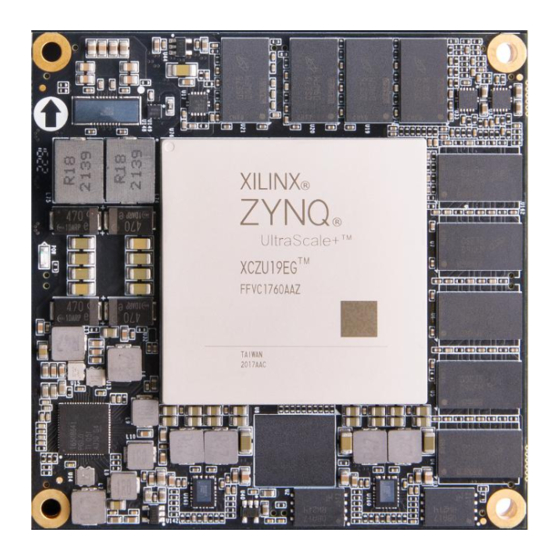
IO ports on the PL side (HP I/O:240,HD I/O:96). The core board size is 80*80 (mm), which is very suitable for secondary development. Front view of core board ACU19EG Part 1.1 ZYNQ Chip The development board uses a series of chips from Xilinx Company's Zynq www.alinx.com 4 / 36... - Page 5 1 instruction and data cache, 1MB level 2 cache, shared by 2 CPUs。 ARM dual-core Cortex-R5 processor, speed up to 533MHz, each CPU 32KB level 1 instruction and data cache, and 128K tightly coupled memory. www.alinx.com 5 / 36...
-
Page 6: Part 1.2 Ddr4 Dram
PS. The maximum operating speed of the DDR4 SDRAM on the PL side can reach 1200MHz (data rate 2400Mbps), and four DDR4 chips are connected to the BANK69,70,71 interfaces of the FPGA. The specific configurations of DDR4 SDRAM on the PS and PL ends are shown in Table 2-3-1. www.alinx.com 6 / 36... - Page 7 The hardware connection method of DDR4 on the PS side is shown in Figure 2-3-1: Figure 2-3-1: PS DDR4 DRAM block diagram The block diagram of DDR4 SDRAM on the PL Side is shown in Figure 2-3-2: Figure 2-3-2: PL DDR4 DRAM block diagram www.alinx.com 7 / 36...
- Page 8 PS_DDR4_DQ4 PS_DDR_DQ4_504 BB31 PS_DDR4_DQ5 PS_DDR_DQ5_504 BB30 PS_DDR4_DQ6 PS_DDR_DQ6_504 BB29 PS_DDR4_DQ7 PS_DDR_DQ7_504 BA31 PS_DDR4_DQ8 PS_DDR_DQ8_504 BB33 PS_DDR4_DQ9 PS_DDR_DQ9_504 BA32 PS_DDR4_DQ10 PS_DDR_DQ10_504 BA33 PS_DDR4_DQ11 PS_DDR_DQ11_504 BB34 PS_DDR4_DQ12 PS_DDR_DQ12_504 AV31 PS_DDR4_DQ13 PS_DDR_DQ13_504 AW32 PS_DDR4_DQ14 PS_DDR_DQ14_504 AV32 PS_DDR4_DQ15 PS_DDR_DQ15_504 AV33 www.alinx.com 8 / 36...
- Page 9 PS_DDR4_DQ40 PS_DDR_DQ40_504 AL37 PS_DDR4_DQ41 PS_DDR_DQ41_504 AL38 PS_DDR4_DQ42 PS_DDR_DQ42_504 AK38 PS_DDR4_DQ43 PS_DDR_DQ43_504 AK39 PS_DDR4_DQ44 PS_DDR_DQ44_504 AJ36 PS_DDR4_DQ45 PS_DDR_DQ45_504 AL35 PS_DDR4_DQ46 PS_DDR_DQ46_504 AJ35 PS_DDR4_DQ47 PS_DDR_DQ47_504 AK35 PS_DDR4_DQ48 PS_DDR_DQ48_504 AR42 PS_DDR4_DQ49 PS_DDR_DQ49_504 AT41 PS_DDR4_DQ50 PS_DDR_DQ50_504 AT42 PS_DDR4_DQ51 PS_DDR_DQ51_504 AT40 www.alinx.com 9 / 36...
- Page 10 PS_DDR4_DM4 PS_DDR_DM4_504 AR39 PS_DDR4_DM5 PS_DDR_DM5_504 AL36 PS_DDR4_DM6 PS_DDR_DM6_504 AU39 PS_DDR4_DM7 PS_DDR_DM7_504 AL42 PS_DDR4_DM8 PS_DDR_DM8_504 AY42 PS_DDR4_A0 PS_DDR_A0_504 BA38 PS_DDR4_A1 PS_DDR_A1_504 BB36 PS_DDR4_A2 PS_DDR_A2_504 BA35 PS_DDR4_A3 PS_DDR_A3_504 BB35 PS_DDR4_A4 PS_DDR_A4_504 BB38 PS_DDR4_A5 PS_DDR_A5_504 AY35 PS_DDR4_A6 PS_DDR_A6_504 AP37 www.alinx.com 10 / 36...
- Page 11 PS_DDR_A14_504 AW35 PL Side DDR4 SDRAM pin assignment: Signal name Pin name Pin number PL_DDR4_DQS0_N IO_L10N_T1U_N7_QBC_AD4N_70 PL_DDR4_DQS0_P IO_L10P_T1U_N6_QBC_AD4P_70 PL_DDR4_DQS1_N IO_L4N_T0U_N7_DBC_AD7N_70 PL_DDR4_DQS1_P IO_L4P_T0U_N6_DBC_AD7P_70 PL_DDR4_DQS2_N IO_L22N_T3U_N7_DBC_AD0N_70 PL_DDR4_DQS2_P IO_L22P_T3U_N6_DBC_AD0P_70 PL_DDR4_DQS3_N IO_L16N_T2U_N7_QBC_AD3N_70 PL_DDR4_DQS3_P IO_L16P_T2U_N6_QBC_AD3P_70 PL_DDR4_DQS4_N IO_L10N_T1U_N7_QBC_AD4N_69 PL_DDR4_DQS4_P IO_L10P_T1U_N6_QBC_AD4P_69 PL_DDR4_DQS5_N IO_L4N_T0U_N7_DBC_AD7N_69 www.alinx.com 11 / 36...
- Page 12 PL_DDR4_DQ13 IO_L5N_T0U_N9_AD14N_70 PL_DDR4_DQ14 IO_L3N_T0L_N5_AD15N_70 PL_DDR4_DQ15 IO_L5P_T0U_N8_AD14P_70 PL_DDR4_DQ16 IO_L20N_T3L_N3_AD1N_70 PL_DDR4_DQ17 IO_L24P_T3U_N10_70 PL_DDR4_DQ18 IO_L21N_T3L_N5_AD8N_70 PL_DDR4_DQ19 IO_L23N_T3U_N9_70 PL_DDR4_DQ20 IO_L20P_T3L_N2_AD1P_70 PL_DDR4_DQ21 IO_L21P_T3L_N4_AD8P_70 PL_DDR4_DQ22 IO_L24N_T3U_N11_70 PL_DDR4_DQ23 IO_L23P_T3U_N8_70 PL_DDR4_DQ24 IO_L15P_T2L_N4_AD11P_70 PL_DDR4_DQ25 IO_L14P_T2L_N2_GC_70 PL_DDR4_DQ26 IO_L17P_T2U_N8_AD10P_70 PL_DDR4_DQ27 IO_L14N_T2L_N3_GC_70 PL_DDR4_DQ28 IO_L15N_T2L_N5_AD11N_70 PL_DDR4_DQ29 IO_L18P_T2U_N10_AD2P_70 PL_DDR4_DQ30 IO_L17N_T2U_N9_AD10N_70 www.alinx.com 12 / 36...
- Page 13 PL_DDR4_DQ49 IO_L21N_T3L_N5_AD8N_69 PL_DDR4_DQ50 IO_L23P_T3U_N8_69 PL_DDR4_DQ51 IO_L20N_T3L_N3_AD1N_69 PL_DDR4_DQ52 IO_L24N_T3U_N11_69 PL_DDR4_DQ53 IO_L20P_T3L_N2_AD1P_69 PL_DDR4_DQ54 IO_L23N_T3U_N9_69 PL_DDR4_DQ55 IO_L21P_T3L_N4_AD8P_69 PL_DDR4_DQ56 IO_L15N_T2L_N5_AD11N_69 PL_DDR4_DQ57 IO_L17N_T2U_N9_AD10N_69 PL_DDR4_DQ58 IO_L15P_T2L_N4_AD11P_69 PL_DDR4_DQ59 IO_L14N_T2L_N3_GC_69 PL_DDR4_DQ60 IO_L14P_T2L_N2_GC_69 PL_DDR4_DQ61 IO_L18N_T2U_N11_AD2N_69 PL_DDR4_DQ62 IO_L17P_T2U_N8_AD10P_69 PL_DDR4_DQ63 IO_L18P_T2U_N10_AD2P_69 PL_DDR4_DM0 IO_L7P_T1L_N0_QBC_AD13P_70 PL_DDR4_DM1 IO_L1P_T0L_N0_DBC_70 PL_DDR4_DM2 IO_L19P_T3L_N0_DBC_AD9P_70 www.alinx.com 13 / 36...
-
Page 14: Part 2.4: Qspi Flash
PL_DDR4_BA0 IO_L10P_T1U_N6_QBC_AD4P_71 PL_DDR4_BA1 IO_L15P_T2L_N4_AD11P_71 PL_DDR4_CAS_B IO_L11N_T1U_N9_GC_71 PL_DDR4_RAS_B IO_L11P_T1U_N8_GC_71 PL_DDR4_CLK_N IO_L13N_T2L_N1_GC_QBC_71 PL_DDR4_CLK_P IO_L13P_T2L_N0_GC_QBC_71 PL_DDR4_BG0 IO_L14N_T2L_N3_GC_71 PL_DDR4_CKE IO_L17N_T2U_N9_AD10N_71 PL_DDR4_RST IO_L14P_T2L_N2_GC_71 Part 2.4: QSPI Flash The ACU19EG core board is equipped with two 512Mbit Quad SPI FLASH chips to www.alinx.com 14 / 36... - Page 15 PS side to function as QSPI FLASH interfaces. Figure 4-1 shows the part of QSPI Flash in the schematic diagram. Figure 2-4-1: QSPI Flash in the schematic Configure chip pin assignments: Signal Name Pin Name Pin Number MIO5_QSPI0_SS_B PS_MIO5_500 AL32 MIO0_QSPI0_SCLK PS_MIO0_500 AM33 MIO4_QSPI0_IO0 PS_MIO4_500 AL33 MIO1_QSPI0_IO1 PS_MIO1_500 AM29 www.alinx.com 15 / 36...
-
Page 16: Part 2.5: Emmc Flash
The eMMC FLASH is connected to MIOs PS side of the ZYNQ UltraScale+. In the system design, it is necessary to configure these GPIO ports on the PS end as EMMC interfaces. Figure 2-5-1 shows the part of eMMC Flash in the schematic diagram. Table 2-5-1: eMMC FLASH Specification www.alinx.com 16 / 36... -
Page 17: Part 2.6: Clock Configuration
Figure 2-6-1: Core Board Clock Source PS System RTC Real Time Clock The crystal of Y1 on the core board provides a 32.768KHz clock source for the RTC real-time. The schematic diagram is shown in Figure 2-6-2: www.alinx.com 17 / 36... - Page 18 The core board provides a differential 200MHz clock source for the reference clock of the DDR4 controller. The clock is connected to the global clock (MRCC) of PL BANK71. The schematic diagram of this clock source is shown in Figure 2-6-4: www.alinx.com 18 / 36...
-
Page 19: Part 2.7: Power Supply
MAX20796GFB+ to provide the core power of 0.85V. a PMIC chip TPS6508640 is used to generate all other power supplies required by the XCZU9EG chip. For the TPS6508640 power supply design, please refer to the power supply chip manual. The design block diagram is as follows : www.alinx.com 19 / 36... - Page 20 ACU19EG User Manual www.alinx.com 20 / 36...
-
Page 21: Part 2.8: Acu19Eg Core Board Form Factors
ACU19EG User Manual Part 2.8: ACU19EG Core Board Form Factors Figure 2-8-1: ACU19EG Core Board Form Factors(Top View) www.alinx.com 21 / 36... - Page 22 131_CLK0_P 131_CLK1_P 131_CLK0_N 131_CLK1_N 131_RX3_P 131_TX3_P 131_RX3_N 131_TX3_N 131_RX2_P 131_TX2_P 131_RX2_N 131_TX2_N 131_RX1_P 131_TX1_P 131_RX1_N 131_TX1_N 131_RX0_P 131_TX0_P 131_RX0_N 131_TX0_N 130_CLK0_P 130_CLK1_P 130_CLK0_N 130_CLK1_N 130_RX3_P 130_TX3_P 130_RX3_N 130_TX3_N 130_RX2_P 130_TX2_P 130_RX2_N 130_TX2_N 130_RX1_P 130_TX1_P 130_RX1_N 130_TX1_N www.alinx.com 22 / 36...
- Page 23 129_RX2_P 129_TX2_P 129_RX2_N 129_TX2_N 129_RX1_P 129_TX1_P 129_RX1_N 129_TX1_N 129_RX0_P 129_TX0_P 129_RX0_N 129_TX0_N 128_CLK0_P AB34 128_CLK1_P AA32 128_CLK0_N AB35 128_CLK1_N AA33 128_RX3_P 128_TX3_P 128_RX3_N 128_TX3_N 128_RX2_P 128_TX2_P 128_RX2_N 128_TX2_N 128_RX1_P 128_TX1_P 128_RX1_N 128_TX1_N 128_RX0_P 128_TX0_P 128_RX0_N 128_TX0_N www.alinx.com 23 / 36...
- Page 24 AG41 505_CLK0_N AG38 505_CLK1_N AE38 505_CLK0_P AG37 505_CLK1_P AE37 DP_HPD_MIO28 DP_AUX_IN_MIO30 DP_OE_MIO29 DP_AUX_OUT_MIO27 PS_IIC1_SDA AG34 USB_DIR PS_IIC1_SCL AH33 USB_CLK SD_CD USB_DATA5 AC32 SD_D1 USB_DATA0 AA30 SD_D2 USB_DATA3 AC31 SD_D3 USB_DATA2 SD_CLK USB_DATA6 AD31 SD_CMD USB_DATA1 AB30 www.alinx.com 24 / 36...
- Page 25 Pin assignment of board to board connector J31 J31 connects the IO of BANK64, BANK65; the maximum voltage standard of BANK64, 65 is 1.8V(BANK power is supplied by carrier board). Signal Name Pin No. Signal Name Pin No. www.alinx.com 25 / 36...
- Page 26 B65_L21_P AM24 B65_L22_P AM23 B65_L19_N AT23 B65_L23_N AL23 B65_L19_P AR23 B65_L23_P AK23 B65_L24_N AK24 B65_L17_N AN28 B65_L24_P AJ24 B65_L17_P AM28 B64_L23_P AJ21 B64_L1_P BA23 B64_L23_N AJ20 B64_L1_N BB23 B64_L24_P AJ22 B64_L16_P AN21 B64_L24_N AK22 B64_L16_N AP21 www.alinx.com 26 / 36...
- Page 27 BANK66, 67 is 1.8V(BANK power is supplied by carrier board). Signal Name Pin No. Signal Name Pin No. B66_L3_P AW17 B66_L4_P BA15 B66_L3_N AW16 B66_L4_N BB15 B66_L1_P AY17 B66_L15_P AU18 B66_L1_N BA17 B66_L15_N AV18 www.alinx.com 27 / 36...
- Page 28 B66_L8_N BB11 B66_L6_N BB13 B67_L23_P AM13 B67_L15_P AR15 B67_L23_N AN13 B67_L15_N AR14 B67_L12_P AT11 B67_L7_P AV12 B67_L12_N AT10 B67_L7_N AW12 B67_L16_P AN12 B67_L11_P AT13 B67_L16_N AP12 B67_L11_N AT12 B67_L14_P AP10 B67_L13_P AR13 B67_L14_N AR10 B67_L13_N AR12 www.alinx.com 28 / 36...
- Page 29 Pin assignment of board to board connector J33 J33 connects the GTH signal of BANK224,225,226,227. Signal Name Pin No. Signal Name Pin No. 224_TX0_N 224_RX0_N 224_TX0_P 224_RX0_P 224_TX1_N 224_RX1_N 224_TX1_P 224_RX1_P 224_TX2_N 224_RX2_N 224_TX2_P 224_RX2_P 224_TX3_N 224_RX3_N 224_TX3_P 224_RX3_P www.alinx.com 29 / 36...
- Page 30 225_TX3_N 225_RX3_N 225_TX3_P 225_RX3_P 225_CLK0_N AH11 225_CLK1_N 225_CLK0_P AH12 225_CLK1_P AG10 226_TX0_N 226_RX0_N 226_TX0_P 226_RX0_P 226_TX1_N 226_RX1_N 226_TX1_P 226_RX1_P 226_TX2_N 226_RX2_N 226_TX2_P 226_RX2_P 226_TX3_N 226_RX3_N 226_TX3_P 226_RX3_P 226_CLK0_N AF11 226_CLK1_N 226_CLK0_P AF12 226_CLK1_P AE10 227_TX0_N 227_RX0_N www.alinx.com 30 / 36...
- Page 31 J34 connects the GTH signal of BANK228,229,230,231. Signal Name Pin No. Signal Name Pin No. 228_TX0_N 228_RX0_N 228_TX0_P 228_RX0_P 228_TX1_N 228_RX1_N 228_TX1_P 228_RX1_P 228_TX2_N 228_RX2_N 228_TX2_P 228_RX2_P 228_TX3_N 228_RX3_N 228_TX3_P 228_RX3_P 228_CLK1_N 228_CLK0_N AB11 228_CLK1_P AA10 228_CLK0_P AB12 229_TX0_N 229_RX0_N 229_TX0_P 229_RX0_P www.alinx.com 31 / 36...
- Page 32 229_TX3_P 229_RX3_P 229_CLK1_N 229_CLK0_N 229_CLK1_P 229_CLK0_P 230_TX0_N 230_RX0_N 230_TX0_P 230_RX0_P 230_TX1_N 230_RX1_N 230_TX1_P 230_RX1_P 230_TX2_N 230_RX2_N 230_TX2_P 230_RX2_P 230_TX3_N 230_RX3_N 230_TX3_P 230_RX3_P 230_CLK1_N 230_CLK0_N 230_CLK1_P 230_CLK0_P 231_TX0_N 231_RX0_N 231_TX0_P 231_RX0_P 231_TX1_N 231_RX1_N 231_TX1_P 231_RX1_P 231_TX2_N 231_RX2_N www.alinx.com 32 / 36...
- Page 33 3.3V. Signal Name Pin No. Signal Name Pin No. +12V +12V +12V +12V +12V +12V +12V +12V +12V +12V +12V +12V +12V +12V +12V B94_L5_N B94_L8_N B94_L5_P B94_L8_P B94_L7_N B94_L12_N B94_L7_P B94_L12_P B94_L3_N B94_L4_N www.alinx.com 33 / 36...
- Page 34 B93_L9_P B93_L5_P B93_L7_N B93_L2_N B93_L7_P B93_L2_P B93_L8_N B93_L4_N B93_L8_P B93_L4_P B93_L3_N B93_L6_N B93_L3_P B93_L6_P B93_L11_N B93_L12_N B93_L11_P B93_L12_P B91_L12_N B91_L7_N B91_L12_P B91_L7_P B91_L5_N B91_L1_N B91_L5_P B91_L1_P B91_L10_N B91_L9_N B91_L10_P B91_L9_P B91_L11_N B91_L2_N B91_L11_P B91_L2_P B91_L3_N B91_L8_N www.alinx.com 34 / 36...
- Page 35 B68_L18_N VCCO_65 B68_L18_P VCCO_65 B68_L12_N B68_L12_P Hang in the air B68_L20_N Hang in the air B68_L20_P Hang in the air B68_L19_N Hang in the air B68_L19_P Hang in the air B68_L22_N Hang in the air B68_L22_P www.alinx.com 35 / 36...
- Page 36 B90_L8_N B68_L5_N B90_L8_P B68_L5_P B90_L11_N B68_L11_N B90_L11_P B68_L11_P B90_L5_N B68_L10_N B90_L5_P B68_L10_P B90_L4_N B68_L8_N B90_L4_P B68_L8_P B90_L3_N B68_L6_N B90_L3_P B68_L6_P B90_L2_N B68_L9_N B90_L2_P B68_L9_P B90_L9_N B68_L3_N B90_L9_P B68_L3_P B90_L6_N B68_L4_N B90_L6_P B68_L4_P B90_L1_N B68_L2_N B90_L1_P B68_L2_P www.alinx.com 36 / 36...
Need help?
Do you have a question about the Zynq UltraScale+MPSoC and is the answer not in the manual?
Questions and answers