
Related Manuals for Performance Computer PT-VME151A

Summary of Contents for Performance Computer PT-VME151A
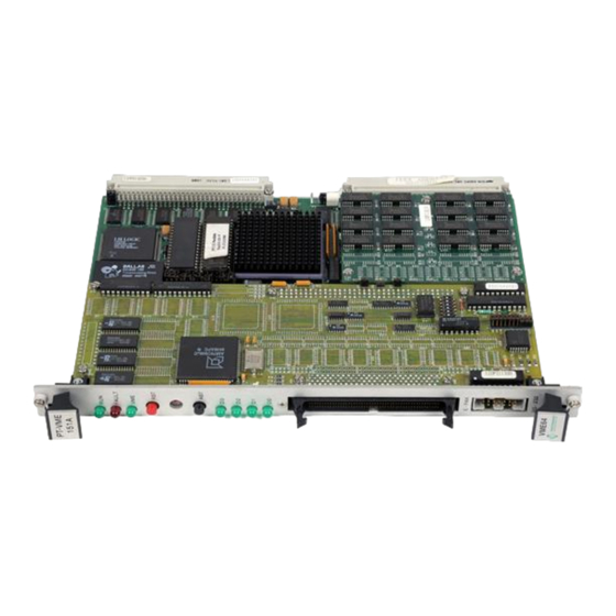
- Page 1 sales@artisantg.com artisantg.com (217) 352-9330 | Click HERE Find the Ribbon / Performance Technologies PT-VME 141 at our website:...
- Page 2 Performance A Performance Technologies Company 315 Science Parkway Computer Rochester, New York USA 14620 USER’S MANUAL PT-VME151A/151AE Extensible Single Board Computer/Controller Document Number 126A0180 Artisan Technology Group - Quality Instrumentation ... Guaranteed | (888) 88-SOURCE | www.artisantg.com...
- Page 3 Technical Publications at (716) 256- 0200 or pccsupport@pt.com. All comments, suggestions, and criticisms are welcome. Copyright Notice © 1993-1994 by Performance Computer, a Performance Technologies Company. -- Printed in USA. 315 Science Parkway, Rochester, New York 14620 Trademarks Microware and OS-9 are trademarks of Microware Systems Corporation.
- Page 4 Although the information contained within this document is considered accurate and characteristic of the subject product, Performance Computer reserves the right to make changes to this document and any prod- ucts described herein to improve reliability, function, or design. Performance Computer does not assume any liability arising out of the application or use of any product or circuit described herein.
- Page 5 Safety Information This section is provided as a summary of the safety recommendations throughout this manual. Perfor- mance Computer (PCC) recommends that all safety precautions are followed to prevent harm to yourself or the equipment. Please follow all warnings marked on the equipment. Safety Precautions •...
-
Page 6: Table Of Contents
Performance Computer Table of Contents Section 1 INTRODUCTION Scope Applicable Documents Model Designations Features Family Members PT-VME131/131E PT-VME141/141E PT-VME151/151E Glossary and Conventions Glossary Conventions Section 2 GETTING STARTED Unpacking and Inspection Hardware Configuration Device Positions “Watchdog” Timer Setup PROM/ROM/SRAM/EEPROM Socket Configuration... - Page 7 Table of Contents Mechanical restraints SCSI device grounds Device addresses Serial Port Cabling Example Mechanical restraints Section 3 FUNCTIONAL DESCRIPTION Microprocessor Memory DRAM DRAM Mapping Sizing Parity Checking Initialization Testing PROM/SRAM Sockets Nonvolatile SRAM and Time of Day/Calendar Clock Serial EEPROM Interval Timer VMEbus Interface DARF64...
- Page 8 Performance Computer Interrupt Handler Local Level 7 Sources Abort SCSI Bus Reset AC Fail System Fail General Purpose Local Interrupts Location Monitor FIFO DARF64 VME Event Timer Event Tick Interval I/O Event FAS216 Requests EPAK Requests (-EPIRQ) EPAK Vectored Interrupt Request DUART Interrupt Request (-INTP<5>)
- Page 9 Table of Contents SCSI DMA Parity Error DARF Parity Error EPAK Parity Error SCSI Present System Status Register 3 DRAM Size Parity Installed Interval Timer Interrupt Pending DUART Utility Serial Ports General Purpose Timer/Counter Parallel Input Port Clear-to-Send Data-Terminal-Ready EPAK General Purpose Input Serial EEPROM Data In Parallel Output Port Request-to-Send...
- Page 10 Performance Computer Interrupt Control Register Maps DARF64 DS1643 Nonvolatile Timekeeping RAM 82C54 Interval Timer EMULEX FAS216 SCSI Controller 68681 DUART Controls and Indicators Rotary Switch “RUN” Indicator “FAULT” Indicator “VME” Indicator RESET Switch ABORT Switch User Programmable LEDs Section 5 CONNECTOR PINOUTS...
- Page 11 Table of Contents The differences between the PT-VME151A and the VME151 Renamed Registers New Devices DRAM Sizing SRAM Access PT-VME151A Differences From VME131/141 DARF64 uses 68040 mode SCSI Controller differences Effects of 68040 vs. 68030 Cacheability and Serialization 68040 Cache Control Registers...
- Page 12 Figure 10: Block Diagram Figure 11: Interval Timer Block Diagram Figure 12: Timer Block Diagram Figure 13: PT-VME151A Front Panel Controls and Indicators Figure 14: DARF Memory Map Extensible Single Board Computer/Controller User’s Manual xi Artisan Technology Group - Quality Instrumentation ... Guaranteed | (888) 88-SOURCE | www.artisantg.com...
- Page 13 List of Figures xii Extensible Single Board Computer/Controller User’s Manual Artisan Technology Group - Quality Instrumentation ... Guaranteed | (888) 88-SOURCE | www.artisantg.com...
- Page 14 Performance Computer List of Tables Table 1: EPAK Caching Options Table 2: Memory Map Table 3: Default VMEbus A24 Memory Map Table 4: Default VMEbus A32 Memory Map Table 5: Interrupt Request Summary Table 6: ACC Register Map Table 7: DARF64 Registers...
- Page 15 List of Tables xiv Extensible Single Board Computer/Controller User’s Manual Artisan Technology Group - Quality Instrumentation ... Guaranteed | (888) 88-SOURCE | www.artisantg.com...
-
Page 16: Section 1 Introduction
PT-VME151A/151AE facilities are presented. Section 1 Provides an introduction and general overview of the PT-VME151A. It is intended as a quick summary of PT-VME151A/151AE features and provides a framework for the rest of the document. -
Page 17: Applicable Documents
Section INTRODUCTION Applicable Documents VMEbus Specification Manual, Revision ANSI/IEEE STD 1014-1987, VMEbus International Trade Association (VITA). VITA; 10229 N. Scottsdale Road, Suite B; Scottsdale, AZ 85253. M68000 Family Programmer’s Reference Manual; M68000PM/AD; Motorola Incorporated, 1989. Motorola Literature Distribution; P.O. Box 20912; Phoenix, AZ 85036. MC68040, MC68EC040, MC68LC040 Microprocessor User’s Manual;... -
Page 18: Model Designations
The PT-VME151A is available with a 25 MHz 68040 microprocessor or a 25 MHz 68EC040 (68040 without MMU or FPU). Additionally, the PT-VME151A has options of 4, 8, 16, 32 or 64 megabytes of main memory. Model designations are as follows:... -
Page 19: Features
Section INTRODUCTION Features • MC68040 Thirty-Two Bit Microprocessor With Internal Cache and FPU PT-VME151 utilizes 25 MHz MC68040 MPU w/Memory Management Unit PT-VME151E utilizes 25 MHz MC68EC040 MPU w/o MMU or FPU MC68030-Compatible Integer Execution Unit MC68881/MC68882-Compatible Floating Point Unit Independent Instruction and Data Memory Management Units 4KByte Physical Instruction Cache and 4KByte Physical Data Cache Accessible Simultaneously Low Latency Bus Accesses for Reduced Cache-Miss Penalty... - Page 20 Performance Computer • General Purpose Local I/O 68681 DUART Dual RS-232 ASYNC Serial I/O ports w/Front Panel Interconnect 16-bit General Purpose Timer 128 Byte EEPROM • DS1643 Nonvolatile Timekeeping RAM 8184 Bytes of Nonvolatile SRAM Real-Time Clock with Integrated Crystal...
-
Page 21: Family Members
A key design criterion was to maintain user software compatibility across the family members. The command and register set of the EMULEX SCSI controller on the PT-VME151A and PT-VME141 is a super set of the PT-VME131’s NCR SCSI controller. The MC68040 of the PT-VME151 is user code compatible with the MC68030 of the PT-VME131 and PT-VME141. -
Page 22: Pt-Vme141/141E
MBytes per second. This high speed transfer capability makes the 141 ideal for applications that require maximum VMEbus utilization. The features of the PT-VME141 and PT-VME141E are identical to the PT-VME151A with the following exceptions: • Advanced Thirty-Two Bit Microprocessor With Internal Cache... -
Page 23: Glossary And Conventions
Section INTRODUCTION Glossary and Conventions Glossary ACC - Advanced VMEbus System Architecture Control Circuit (CA91C014). CPU - Central Processing Unit (MC68040 or MC68EC040) DARF64 - Data Address Register File (CA91C064). DMA - Direct Memory Access, hardware controller block data transfers. DMAC - Direct Memory Access Controller. -
Page 24: Conventions
Performance Computer Conventions Upper case names enclosed in square brackets ([,]) represent signal names that can be found in the sche- matics. Numbers enclosed in “less than” (<) and “greater than” (>) symbols refer to individual bits of a signal bus. - Page 25 Section INTRODUCTION 10 Extensible Single Board Computer/Controller User’s Manual Artisan Technology Group - Quality Instrumentation ... Guaranteed | (888) 88-SOURCE | www.artisantg.com...
-
Page 26: Section 2 Getting Started
If no external damage is visible, carefully unpack contents from shipping carton, observing anti-static precautions identified above and verify against packing list. Inspect the PT-VME151A for any visible signs of shipping damage. If such physical damage is noted, report it immediately to Performance Tech- nologies or appropriate agent. -
Page 27: Hardware Configuration
A layout for the PT-VME151A/151AE is shown in “Figure 1: PT-VME151A/151AE Device Positions”. The model PT-VME151A and PT-VME151AE are two versions of the same PCB with different compo- nent options. There are various jumpers to configure user options which must be set before initial bootup. -
Page 28: Watchdog" Timer Setup
“watchdog” timer will cause a local reset to occur, unless reset every two seconds by software. Jumper Block K1 consists of a single pair of pins that is either open or shorted. See “Figure 1: PT-VME151A/ 151AE Device Positions” on page 12. -
Page 29: Prom/Rom/Sram/Eeprom Socket Configuration
Section GETTING STARTED PROM/ROM/SRAM/EEPROM Socket Configuration Locations U23 and U38 both provide support for read only devices such as ROM, PROM, EPROM, and Flash EPROM. Location U23 has additional support for read/write devices as well, SRAM and non-vola- tile SRAM. The positions of locations U23 and U38 are identified in Figure 1: on page 12 and Figure 2: on page 14. -
Page 30: Location U23 Setup
Performance Computer Location U23 Setup Figure 3: K4 and K10Jumpers The pin out configuration for location U23 is defined by Jumper Blocks K4 and K10. There are eleven jumpers at location K4 and a single jumper at K10. Each K4 jumper position consists of a row of three adjacent pins. The... -
Page 31: Figure 5: U23 And U38 Jumper Settings
Figure 5 displays Jumper Blocks K10, K4, K11, and K3 from the component side of the PCB. The pattern represented below is viewed when the PT-VME151A/151AE is placed on a work surface component side up and the Front Panel closest to the observer. “*” indicates factory configuration. -
Page 32: Scsi Termination
Fuse Resistor Packs Disabling Termination If the PT-VME151A is not at one end of the SCSI cable then the termination will be supplied by another SCSI device and, SCSI Termination resistor packages RP1 and RP2 (shown above) must be removed. - Page 33 SCSIbus termination. The SCSI TERMPWR mechanism provided the solu- tion. The PT-VME151A’s +5V supply goes through fuse F1 then diode CR2 to be OR’ed into the SCSI TERMPWR signal. This allows the PT-VME151A to supply SCSIbus termination power when it is powered up and some other device on the SCSIbus to provide it when it is not.
-
Page 34: Dram Module Upgrading
Optional EPAK PT-VME151A Base Module To install the new DRAM module, place the PT-VME151A on a work surface component side up. Care- fully align the bodies of the DRAM module connectors, and press firmly on top of the connector with both thumbs to snap it in. -
Page 35: Epak Installation
Section GETTING STARTED NOTE: All 3 standoffs must be properly installed because they are also used to carry power and ground to the DRAM Module. EPAK Installation If not already installed do it now! Follow the instructions contained in your EPAK Users Manual. 20 Extensible Single Board Computer/Controller User’s Manual Artisan Technology Group - Quality Instrumentation ... -
Page 36: Board Installation
Board Installation Power Considerations The PT-VME151A typically draws 25 ma. of +12V and -12V, and 3.9 Amps of +5V. These figures must be added to those of any attached EPAK or EBOARD to determine the total power requirements. It is recommended that Maximum values are used to ensure adequate margins. -
Page 37: Figure 7: Pt-Vme151A Front Panel
Section GETTING STARTED Figure 7: PT-VME151A Front Panel Captive Chassis Mount Screw PT-VME Ejector Handle 151A System Status Indicators RESET Switch Rotary Switch ABORT Switch User Programmable LEDs Optional EPAK I/O Connector RS-232 Utility Port VME64 Ejector Handle Performance Technologies Captive Chassis Mount Screw 22 Extensible Single Board Computer/Controller User’s Manual... -
Page 38: Scsi Considerations
The PT-VME151A SCSI interconnect is provided through the User Defined Signal pins of the VMEbus P2 connector. The signals are organized so that a mass terminated Insulation Displacement Connectors (IDC) can be used to attach SCSI devices to the PT-VME151A. See “Table 14: VMEbus” P2” Connec- tions” on page 77. -
Page 39: Mechanical Restraints
Section GETTING STARTED AMP 1-746288-0 (connector) AMP 499252-4 (strain relief) Figure 8: Example SCSI Cable 6 Meter Maximum A B C Pin 1 Indicator 50 Conductor Ribbon Cable 50 Pin Flat Cable Connectors for SCSI devices (up to 7) 64 Pin VMEbus “P2” Connector Mechanical restraints Depending upon your mechanical configuration, tie wraps or cable clamps may be necessary to provide mechanical support for the cable. -
Page 40: Device Addresses
Following is an example cable with vendors and part numbers for the components. These configurations have been tested at PTI. Figure 9 displays an example serial cable for the PT-VME151A. The view is with the connector sockets pointing towards you. -
Page 41: Mechanical Restraints
Section GETTING STARTED Burndy FRS14BF-8 (strain relief included) or AMP 746288-2 (connector) AMP 499252-9 (strain relief) Figure 9: Example Serial port Cable 50 Foot Maximum Pin 1 Indicator 14 Conductor Ribbon Cable 14 Pin Flat Cable Connector 25 Pin D-Shell Connector Mechanical restraints Depending upon your mechanical configuration, tie wraps or cable clamps may be necessary to provide mechanical support for the cable. -
Page 42: Section 3 Functional Description
Section FUNCTIONAL DESCRIPTION A block diagram of the PT-VME151A/151AE is provided below. Down the center are the 32-bit micro- processor address and data busses. To the right is an 8-bit buffered data bus that provides I/O interface connectivity. To the left is the VMEbus interface, provided by the Advanced VMEbus Interface Chip Set. -
Page 43: Microprocessor
The 68040 and 68EC040 support a burst mode for filling their on-chip data and instruction caches. The PT-VME151A utilizes the fast page mode of the DRAM to accelerate the burst transfer operation. During a burst transfer four sequential long words are fetched from the DRAM, requiring four clock cycles for the first long word transfer and two clock cycles for subsequent long word fetches. -
Page 44: Dram Mapping
Performance Computer DRAM Mapping DRAM Size Address Range Response 4 MBytes 20000000-203FFFFFh Normal 20400000-20FFFFFFh Blank 21000000-213FFFFFh Normal - repeat of 20000000-203FFFFF 21400000-21FFFFFFh Blank The pattern of (4M Normal) - (12M Blank) - (4M Normal) - (12M Blank) repeats throughout the range of 20000000-2FFFFFFFh. Thus address 20000000h may be read or written at 21000000h, 22000000h, etc. -
Page 45: Parity
DARF64 or SCSI controller reference will assert the L7IMEM pin of the ACC, gener- ating a level 7 interrupt request. The source of the a parity error is latched in PT-VME151A System Status Register 2. Parity errors that generate a Bus Error (68040 and EPAK bus masters) will not generate a Level 7 interrupt however, the source of the error will be latched in Status Register 2. -
Page 46: Initialization
Performance Technologies normally uses this memory to store various parameters and options used in the initialization and operation of the PT-VME151A. This device is socketed so that it can be moved to another board if necessary. For instance, if board level replacement is typically performed on failures in the field, the EEPROM can be moved to the replace- ment board to maintain the configuration information of the original board. -
Page 47: Interval Timer
Section FUNCTIONAL DESCRIPTION Interval Timer The Interval Timer, an Intel 82C54, provides three independent 16-bit timers running off the same 4 MHz clock. These three timers are identical in operation. Refer to the Intel Peripherals Handbook for a complete description of the 82C54 When an Interval Timer is programmed in “Mode 2”, it will perform the following functions when it counts down to zero: pulse its OUTPUT pin, reload the initial count, and continue counting. -
Page 48: Vmebus Interface
The DARF64 is a 64-bit Data/Address Register File which interfaces the VMEbus address and data buses with the local PT-VME151A bus. It may act as a VMEbus Master or Slave. The local DRAM and EPAK address spaces of the PT-VME151A are accessible to a VMEbus Master through the DARF64. The DARF64 is also capable of DMA transfers between local memory (DRAM or EPAK) and the VMEbus. -
Page 49: Decoupled
Section FUNCTIONAL DESCRIPTION All read, read-modify-write, and interrupt acknowledge cycles are atomic. To preserve data integ- rity, atomic cycles are not performed until all write cycles queued ahead of the atomic cycle are completed. Decoupled This feature allows transfers on the VMEbus to be completely “decoupled” from any latencies incurred on the local bus. -
Page 50: Vmebus Slave Accesses
The Slave Image is the VMEbus address range throughout which the local memory of the board can be accessed. The slave image of the PT-VME151A is defined in programmable registers of the DARF64. Separate slave images, different in size, can be set up in the A64, A32 and A24 address spaces. -
Page 51: Read-Modify-Write
FFFFFFFFh. In order to access the full VMEbus address space the Page bit in the 151A System Control Register defines VMEbus address bit 31. When the Page bit is 0, PT-VME151A addresses 80000000h-FFFFFFFFh are mapped to VMEbus addresses 00000000h - 7FFFFFFFh. -
Page 52: Location Monitor
A32 and A24 slave images. The monitor is equally accessible by the VMEbus and the local CPU. A process on the PT-VME151A does not need to determine whether the process it’s sending a message to is local or not. -
Page 53: Acc
Register Block. Reset The Reset block provides control of the PT-VME151A local reset signal [-LRST]. Local Reset is asserted when the PT-VME151A detects a power on condition, if VMEbus [SYSRST*] is asserted, the front panel Reset button is pressed, the watchdog timer expires, or software sets the SWRST bit in the ACC General Control Register. -
Page 54: Tick Timer
Performance Computer before the 2 seconds delay expires results in the assertion of Local Reset [-LRST]. Local Reset initializes the 68040 and all I/O devices on the PT-VME151A. The Watchdog Timer can be disabled by jumper K1. Tick Timer The Tick Timer is a user programmable timer in the ACC. It can be set to one of two different modes by the TICKM bit in the ACC Control and Status Register: normal or fast. -
Page 55: Abort
If the VMEbus [ACFAIL*] signal is asserted an interrupt can be generated to the 68040. The AC Failure warning allows the PT-VME151A software to execute appropriate shut- down procedures. The interrupt is enabled by setting the ACFIS bit in the ACC Level 7 Interrupt Status Register. -
Page 56: Location Monitor Fifo
Performance Computer “vectored” for the EPAK and DUART interfaces. The vector is supplied by the interrupting device, not the AVICS 64, during the interrupt acknowledge cycle. Location Monitor FIFO This interrupt indicates that there are entries in the DARF64 Location Monitor FIFO. It will remain active until the FIFO becomes empty. -
Page 57: Tick
Section FUNCTIONAL DESCRIPTION The ACC interrupt input is driven by the logical OR of the ACC TICK output and the 82C54 interrupt output. System Status Register 3 identifies the source of the Timer Event. After reset, the Tick Timer interrupts are enabled and the Interval Timer interrupts are disabled to maintain compatibility with PT-VME151. -
Page 58: Epak Vectored Interrupt Request
“auto-vectored” interrupt is presented to the 68040. The EPAK [-EPVIR] signal drives the ACC interrupt input pin -LIRQ4 through signal line [-INTP<4>]. CAUTION: Due to the PT-VME151A/151AE hardware implementation the “vectored” option must always be used for the ACC Local Interrupts 5 and 4 Control Register 4AV bit. -
Page 59: Interrupt Acknowledgment
ACC enables itself as the VMEbus System Controller. The System Controller functions will be enabled automatically if the PT-VME151A is in slot 1 and [BG3IN*] is open. Software can determine if this has occurred by reading the SYSC status bit of the ACC Status Register 1. -
Page 60: Iack Daisy Chain Driver
I/O UTILITIES System Control Registers The System Control Registers provide the PT-VME151A with miscellaneous control functions not provided in other registers. They are all 8-bit, read/write registers. These registers can be read back. This allows the use of AND or OR instructions to clear and set indi- vidual bits. -
Page 61: Vmebus Page Select
System Control Register is used to define VMEbus address bit 31. When the VMEbus Page Select bit is 0, PT-VME151A addresses 80000000h-FFFFFFFFh are mapped to VMEbus addresses 00000000h - 7FFFFFFFh. When the VMEbus Page Select bit is 1, PT-VME151A addresses 80000000h-FFFFFFFFh are mapped to VMEbus addresses 80000000h-FFFFFFFFh. -
Page 62: System Control Register 2
A32SIZ field of the DARF VMEBAR register is programmed to allow a A32 Slave Image Size greater than or equal to 32MBytes (Dh). In this case a portion of the PT-VME151A slave image is replaced by the EPAK’s address space. When EPAK accesses from the VMEbus are disabled, all of the PT-VME151A installed DRAM may be accessed by a VMEbus master. - Page 63 Section FUNCTIONAL DESCRIPTION [Move data with bad parity to DRAM addresses] move.b #$02,$50000000 ;Clear EBP and Set EPEC EBP is always cleared at reset allowing good parity to be written. EBP is register bit 2. 48 Extensible Single Board Computer/Controller User’s Manual Artisan Technology Group - Quality Instrumentation ...
-
Page 64: Enable Interval Timer Interrupts
Performance Computer Reset Interval Timer Interrupts The RITI bits are encoded to reset the Request Latch of the individual Interval Timers. When an Interval Timer reaches it’s terminal count, the event is recorded by its Request Latch. The outputs of the three Request Latches are OR’ed together, generating the Interval Timer Interrupt Request to the 68040. -
Page 65: System Status Registers
FUNCTIONAL DESCRIPTION System Status Registers The System Status register provides the PT-VME151A with status information not provided in other registers. It is a read only register. All unused bits (31-4) should be masked to zero (0) for future expan- sion. -
Page 66: Epak Parity Error
The DRAM Size field (named DRAMSZ) indicates the size of the DRAM module installed on the PT-VME151A base board. DRAMSZ is a three bit field. It consists of register bits 0 through 2, where bit 0 is the least significant bit. The following table elaborates the possible values:... -
Page 67: Duart
I/O. If you recieved a Performance Computer Debugger (PTBUG) as part of your order, Port A of the DUART will be set to 9600 baud, 1 stop bit, no parity. PTBUG ignores CTS and DTR and deasserts RTS and DSR (false). -
Page 68: Epak General Purpose Input
Performance Computer EPAK General Purpose Input Parallel Input 3 of the DUART is attached to the EPAK +EPKIO signal. The state of this control signal can be read from the IP3 bit (3) of the DUART Input Port Register. The function of this pin is determined by the attached EPAK Expansion Module. -
Page 69: Serial Eeprom Data Out
Section FUNCTIONAL DESCRIPTION Serial EEPROM Data Out Parallel Output 7 of the DUART is attached to the Data In (DI) pin of the 93C46 Serial EEPROM. Programmed I/O can control the state of this signal with OPR7 bit (7) of the DUART Output Port Register. -
Page 70: Scsi Controller
The SCSI interface is through the P2 VME connector. Termination is provided by optional plug-in resistor packs. The resistor packs should be installed if the PT-VME151A is at either end of a SCSI cable. Conversely, the resistor packs should be removed if the PT-VME151A is installed in the middle of the SCSI cable. -
Page 71: Dma Mechanism
Fuse F1 (Littelfuse Part No. 273-001) provides short circuit protection for TERMPWR. To remove the fuse, place the PT-VME151A on a work surface component side up with the VMEbus connectors closest to the observer. Grip the clear body of fuse F1 and pull to the right. To replace the fuse reverse the 56 Extensible Single Board Computer/Controller User’s Manual... - Page 72 Performance Computer process. The bidirectional arrow in “Figure 6: SCSI Components” on page 17 shows the direction of motion. See “TERMPWR Overview” on page 17 for a discussion of the uses of TERMPWR. Extensible Single Board Computer/Controller User’s Manual 57...
-
Page 73: Epak Interface
SRAM or registers on an EPAK. The EPAK may be accessed form the VMEbus as part of the PT-VME151A address space. To do so, VMEbus address bit A24 must be 1, the EEAV bit in System Control Register 2 must be 0, and the A32SIZ field of the DARF VMEBAR register must be programmed to allow an A32 Slave Image Size greater than or equal to 32MBytes (Dh). -
Page 74: Section 4 Functional Summary
Section FUNCTIONAL SUMMARY Memory Map Table 2 describes the location of all configuration and operational registers of the PT-VME151A as seen by the MC68040. The sizing column indicates if the device supports data bus sizing. Table 2: Memory Map ADDRESS RANGE... -
Page 75: Default Vmebus Slave Addressing
VMEbus master. The A32SIZ field of the DARF VMEBAR register must be re- programmed to allow an A32 Slave Image Size greater than or equal to 32MBytes (Dh). Table 3 describes the default address map of the PT-VME151A as seen by a VMEbus master using A24 addressing. -
Page 76: 151A System Registers
Performance Computer 151A System Registers There are six registers on the PT-VME151A that are not defined in the referenced data sheets. These registers are unique to the PT-VME151A, providing control of major functional blocks and status. System Control Register 1... - Page 77 Section FUNCTIONAL SUMMARY Enable 68040 caching of VMEbus accesses. See “PT-VME151A Control Register Differences” on page 93 for in-depth discussion. Disable caching Enable caching 62 Extensible Single Board Computer/Controller User’s Manual Artisan Technology Group - Quality Instrumentation ... Guaranteed | (888) 88-SOURCE | www.artisantg.com...
- Page 78 Performance Computer System Control Register 2 Address 50000000h Byte Read/Write Only All bits cleared to zero by reset, except ETTI EEAV EPEC RITI EITI ETTI Reserved Name Function EEAV Enable EPAK Access from VMEbus Enable EPAK Access from VMEbus when A24 = 1...
-
Page 79: System Status Register 1
SRAM Size No SRAM installed Reserved, mask to zero when read The PT-VME151A does not support SRAM so this field is always read as zero. This provides backwards compat- ibility with the PT-VME151. 64 Extensible Single Board Computer/Controller User’s Manual... -
Page 80: System Status Register 2
Performance Computer System Status Register 2 Address 60000000h Byte Read Only Reserved 40PE SCSIPE DARFPE EPAKPE SCSIP Reserved Name Function Reserved, mask to zero when read 40PE 68040 Parity Error A parity error was detected during a 68040 DRAM read... -
Page 81: System Status Register 3
Section FUNCTIONAL SUMMARY System Status Register 3 Address 68000000h Byte Read Only DRAMSZ PARI ITIP0 ITIP1 ITIP2 Reserved Name Function DRAMSZ Indicates the amount of DRAM installed Reserved 64 Meg 32 Meg 16 Meg 8 Meg 4 Meg PARI Parity Installed Parity generation and checking logic installed Parity logic not installed - no parity errors generated ITIP0... -
Page 82: Scsi Memory Address Register
The SCSI Memory Address Register is written with the starting address for a SCSI DMA transfer. The register retains its value after reset and is unde- fined after power up Jumper List (Defaults) This section provides a summary of the jumpers on the PT-VME151A/151AE and their default settings. JUMPER DEFAULT FUNCTION... -
Page 83: Interrupt Control
Section FUNCTIONAL SUMMARY Interrupt Control The ACC controls local and VMEbus interrupts. Because the ACC allows the dynamic assignment of local interrupts to specific request levels, a fixed interrupt map is unnecessary. The following table lists the internal and VMEbus interrupt sources and the levels to which they may be assigned. The ACC inter- rupt input pin for each local interrupt request is also shown. -
Page 84: Register Maps
PTI for our applications. All “INIT” values are in hexadecimal, registers that are “don’t care” at initialization time contain a hyphen. See “APPENDIX F: PT-VME151A Differences From VME131/141” on page 91 for in-depth discus- sion of initialization issues. See APPENDIX G: and APPENDIX H: for more information. -
Page 85: Darf64
Section FUNCTIONAL SUMMARY DARF64 See “APPENDIX F: PT-VME151A Differences From VME131/141” on page 91 for in-depth discussion of initialization issues. See APPENDIX G: and APPENDIX H: for more information. Table 7: DARF64 Registers ADDRESS NAME FUNCTION INIT 18000000h DMALAR DMA Local Address Register... -
Page 86: Ds1643 Nonvolatile Timekeeping Ram
Performance Computer DS1643 Nonvolatile Timekeeping RAM Table 8: DS1643 Nonvolatile Timekeeping RAM Registers ADDRESS FUNCTION VALUES INIT 0F000000h- Nonvolatile RAM User Definable 0F001FF7h 0F001FF8h Control Register 0F001FF9h Seconds 00-59 msb = 0 0F001FFAh Minutes 00-59 0F001FFBh Hours 00-23 0F001FFCh 01-07... -
Page 87: Emulex Fas216 Scsi Controller
Section FUNCTIONAL SUMMARY EMULEX FAS216 SCSI Controller Table 10: EMULEX FAS216 SCSI Controller Register Map ADDRESS READ FUNCTION WRITE FUNCTION INIT 0A000000h Transfer Counter Low Transfer Count Low 0A000001h Transfer Counter Mid Transfer Count Mid 0A000002h FIFO FIFO 0A000003h Command Command 0A000004h Status... -
Page 88: Controls And Indicators
Performance Computer Controls and Indicators The figure below identifies the controls and indicators that reside on the PT-VME151A Front Panel. Figure 13: PT-VME151A Front Panel Controls and Indicators PT-VME 151A “RUN” Indicator “FAULT” Indicator “VME” Indicator RESET Switch Rotary Switch... -
Page 89: Run" Indicator
This green indicator is illuminated during the period of a VMEbus master access attempt. The LED illu- mination intensity is a relative indication of the PT-VME151A’s VMEbus access frequency. A solid, bright light is indicative of high bus contention where the PT-VME151A is not receiving a Bus Grant. RESET Switch The reset switch is a red push button on the front panel which is tied to the EXTRST input pin of the ACC which in turn generates a board reset [-LRST]. -
Page 90: Section 5 Connector Pinouts
Section CONNECTOR PINOUTS Utility Serial Port Pin Assignments Connections to the Debug/Utility port can be made using the supplied cable. A Data Terminal Equipment RS-232C interface is provided. A transition cable is supplied which converts between the 14-pin header (P3) and a female shell (male pin) 25-pin D-Shell connector. Table 12: Utility Serial Port Pin Assignments DB 25 Pin Circuit... -
Page 91: Vmebus Pin Assignments
Section CONNECTOR PINOUTS VMEbus Pin Assignments Table 13: VMEbus “P1” Connections Signal Signal Signal BBSY* BCLR* ACFAIL* BG0IN* BG0OUT* BG1IN* BG1OUT* BG2IN* BG2OUT* SYSCLK BG3IN* SYSFAIL* BG3OUT* BERR DS1* BR0* SYSRESET* DS0* BR1* LWORD* WRITE* BR2* BR3* DTACK* IACK* IACKIN* IACKOUT* IRQ7* IRQ6*... -
Page 92: Table 14: Vmebus" P2" Connections
VRMC* TPWR VMEbus P2 connector rows A and C are User Definable connector pins. The PT-VME151A provides the connections identified above for the SCSIbus interconnect. NOTE: VRMC* is a jumper (K7) selectable option. The IEEE 1014 Rev C VMEbus Specification defines this signal as “RESERVED”. -
Page 93: Epak Connectors
Section CONNECTOR PINOUTS EPAK Connectors The PT-VME151A EPAK module interface is comprised of connectors J1, J2, and J3, and the six EPAK standoffs. Table 15: EPAK Connections Signal Signal Signal +MPSZ0 +MPA24 +MPSZ1 +MPA25 +MPFC0 +MPA26 +MPA00 +MPFC1 +MPA27 +MPA01... -
Page 94: Dram Module
Performance Computer The EPAK mounting standoffs are used to carry power and ground to the EPAK module. Table 16: EPAK mounting standoffs Mounting pin Signal DRAM Module The DRAM Module standoff carries ground to the module.] Table 17: DRAM Module Connections... -
Page 95: Table 18: Epak Mounting Standoffs
Section CONNECTOR PINOUTS Table 17: DRAM Module Connections Signal Signal RAS2 RAS3 PTST RASP The DRAM mounting standoffs are used to carry power and ground to the DRAM module. Table 18: EPAK mounting standoffs Mounting pin Signal 80 Extensible Single Board Computer/Controller User’s Manual Artisan Technology Group - Quality Instrumentation ... -
Page 96: Section 6 Mechanical And Environmental
Section MECHANICAL AND ENVIRONMENTAL Power Requirements The following values are without an EPAK installed. Table 19: Power Requirements Voltage Typical Maximum +5V (±5%) 3.9 Amps 4.4 Amps +12V (±5%) 25 mA 42 mA -12V (±5%) 25 mA 42 mA Ambient Temperature Table 20: Ambient Temperature Minimum Maximum... -
Page 97: Mechanical Shock
Section MECHANICAL AND ENVIRONMENTAL Mechanical Shock Designed to meet 20g for 6 ms (half sine). Physical Dimensions Base board only Table 22: Physical Dimensions Dimension Millimeters Inches Width Depth Front Panel 20.3 Component Height 82 Extensible Single Board Computer/Controller User’s Manual Artisan Technology Group - Quality Instrumentation ... -
Page 98: Section 7 Appendices
APPENDICES APPENDIX A: Product Warranty Performance Computer, A Performance Technologies Company (hereinafter “PCC”) warrants that its products sold hereunder will at the time of shipment be free from defects in material and workmanship and will conform to PCC’s applicable specifica- tions or, if appropriate, to Buyer’s specifications accepted by PCC in writing. -
Page 99: Product Return Procedure
Section APPENDICES APPENDIX B: Product Return Procedure If you find that your Performance Computer (“PCC”) product must be returned for repair, note the following: To return equipment, please obtain a Return Material Authorization (RMA) number. PCC cannot accept returns without an RMA number. -
Page 100: Installation Notes
SENSITIVE TO STATIC ELECTRICITY. ORDINARY AMOUNTS OF STATIC ELECTRICITY GENERATED BY YOUR CLOTHING OR WORK ENVIRONMENT CAN DAMAGE THE ELEC- TRONIC EQUIPMENT. IT IS RECOMMENDED THAT WHEN INSTALLING THE PT-VME151A IN A SYSTEM OR THE COMPONENTS ON THE BOARD ITSELF THAT ANTI-STATIC GROUNDING STRAPS AND ANTI-STATIC MATS ARE USED TO HELP PREVENT DAMAGE DUE TO ELECTROSTATIC DISCHARGE. -
Page 101: Eeprom Usage
EEPROM as a result of running factory testing of the PT-VME151A. The table is divided into two groups, locations 00-43h are used by PTbug (however the information that they contain will probably be necessary for any application) and locations 44h-63h are used by OS-9™... -
Page 102: Table 23: Eeprom Default Values
Performance Computer OS-9 PTI offers the OS-9 Real-Time Operating System from Microware Systems Corporation for the PT- VME151A. Locations 44h through 63h are used by OS-9 if installed. For more information contact PTI or Microware. Address: Microware Systems Corporation; 1900 N. W. 114th Street; Des Moines, Iowa 50325. - Page 103 Section APPENDICES Table 23: EEPROM Default Values Address Length Default Description 1 byte Floppy Format 8 bytes “shell” Shell String 2 bytes $0400 Number Of 256 Byte RAM Disk Sectors 2 bytes $0000 SCSI Master/Slave Boot (Slave) 6 bytes XX XX XX Ethernet Link-Level (Physical) Address XX XX 4 bytes...
-
Page 104: Renamed Registers
Software may determine whether it is running on a PT-VME151 or a PT-VME151A by reading one of the new device registers. If a no Bus Error occurs then the code is running on a PT-VME151A. A summary of the new register assignment follows:... -
Page 105: Sram Access
APPENDICES SRAM Access The PT-VME151A does not support the SRAM option that was available on the 151. As a result the SRSZ field in System Status Register 1 will always return 0, indicating that NO SRAM is installed. On the 151 accesses to address space allocated to the SRAM would never generate a Bus Error. Accesses to the same space on the PT-VME151A will terminate with a local Bus Error. -
Page 106: Vme151A Differences From Vme131/141
DARF64 uses 68040 mode The PT-VME151A is configured in hardware to automatically come up in 68040 mode. This means that a read from the DARF64 Mode Control Register will show a 1 in bit 24 (040 mode enabled) instead of 0 (as in VME141). -
Page 107: 68040 Cache Control Registers
Section APPENDICES Problems may arise with I/O devices where a read from a data register may depend on a write to a different register. In these cases, because the addresses are different, the 68040 has no way of deter- mining the dependency of the read and write instructions so that the register read may occur before the write. -
Page 108: 68040 Cache Clearing
EPAK would then also depend on the state of the Enable EPAK Caching bit of the Control Register. In summary, in normal PT-VME151A operation with existing EPAKs, EPAK address space is defined internal to the 68040 as noncachable. This makes the Enable EPAK Caching bit of the Control Register irrelevant. - Page 109 Section APPENDICES discarding the data it doesn’t need. This could have adverse effects on VMEbus bandwidth since the PT- VME151A could be doing four times as many reads as it needs. If this situation occurs, the only solutions are to disable all data caching (using the 68040 Cache Control Register) or to use the MMU of the 68040 to make VME space noncacheable.
-
Page 110: Avics Overview
Performance Computer APPENDIX G: AVICS Overview The Advanced VMEbus Interface Chip Set (AVICS) consists of two distinct integrated circuits: the Advanced System Architecture Control Circuit (the ACC) and the Data/Address Register File VME64 (the DARF64). This pair of ICs integrates all the functions commonly required to interface an intelligent card to the VMEbus, while adding features that provide major architectural improvements including the capability to perform 64-bit transfers (VME64). -
Page 111: Location Monitor
Section APPENDICES The internal registers of the DARF64 and ACC are fully accessible by the local CPU while in BI- mode. The slave image of local memory, at the programmed base address and size, is also accessible to the CPU, since such an access does not use the VMEbus or FIFOs unless the DARF64 is in loop- back mode (described in the “Test and Diagnostic Modes”... -
Page 112: Figure 14: Darf Memory Map
Performance Computer Figure 14: DARF Memory Map FFFFFFFFh Page 31 A16:D16 Location 64 KBytes FFFF0000h Page 30, A32:D32 Page 29, A32:D32 Page 28, A32:D32 96 MBytes Page 27, A32:D32 Less A32:D32 Space 64 KBytes Page 26, A32:D32 Page 25, A32:D32... -
Page 113: Master Vmebus Accesses
Section APPENDICES The A16:D16 region is located at the top of the memory map, in the last 64Kb (FFFF0000h- FFFFFFFFh). This space can be disabled using the A16DI bit in the DARF64 Mode Control Register, in which case that address range becomes A32:D32. If the A16 region is enabled and the CPU accesses that region, the DARF64 will perform the cycle on the VMEbus with address bits 31 through 16 set to one, and will use the address modifier codes indicating short addressing. -
Page 114: Slave Vmebus Accesses
Performance Computer The transmit and receive channels of the DARF64 can each be programmed to operate in atomic or decoupled mode by using the RXATOM and TXATOM bits in the DARF Mode Control Register. Read cycles and interrupt acknowledge cycles are always atomic. In atomic mode accesses, the CPU transfer is not enqueued by the transmit FIFO;... - Page 115 Section APPENDICES directly by the CPU, or by the CPU via one of its slave images, or by the VMEbus through the DARF64, the same memory locations are selected. Otherwise, it is possible that different areas of local memory could be accessed through those three paths. The restriction on the slave image base is that it must be a multiple of the amount of memory installed on the CPU card.
-
Page 116: Avics Application Notes
L7I0) interrupts can be masked. All interrupts are autovectored, except for LIRQ4 and LIRQ5 which can be programmed to be vectored or autovectored. Example: The following interrupt assignments are recommended for a PT-VME151A/151AE board: Table 26: Recommended Interrupt Assignments Signal Source*... -
Page 117: Setting Up The Master Bus Memory Map
Section APPENDICES Setting Up the Master Bus Memory Map When the host accesses the VMEbus, the address used by the CPU determines the address and data modes the DARF will use to perform the cycle. All outgoing VMEbus accesses are affected by a programmed memory map. -
Page 118: Example A
Performance Computer CAUTION: The A24 base address must be a multiple of the amount of memory installed on board. Step 2 Select the desired address protection boundary by entering the required value into DARF Access Protect Boundary Register. Step 3 Set the A24SLVEN bit (located in the DARF Mode Control Register) if an A24 image is desired;... -
Page 119: Example B
Step 7 Clear the VPG bit of the PT-VME151A System Control Register (address $0D000000) to select access of lower 2GB VMEbus space. Write the value 0 (word or longword only) to address 883FFFFCh, disabling BI-mode by writing to the location monitor (with bit 31 of the address set). -
Page 120: Generating Vmebus Interrupts
Performance Computer another board can get at the location monitor in A24 space at any address with a valid A24 address modifier. Step 8 Do a dummy read from DARF Location Monitor FIFO Read Port to clear the previous loca- tion monitor entry. -
Page 121: Initiating A Dma Transfer
Section APPENDICES Initiating a DMA Transfer Step 1 Make sure the system is not in BI-mode (refer to steps 7-9 of “Setting Up A24/A32 Slave Images on the Bus” on page 102). Step 2 Set the DARFEN bit (located in the DARF Mode Control Register) to enable DARF64 functions. - Page 122 Performance Computer Step 6 Set the DMA24 bit of DARF Mode Control Register to enable the DMA to operate as an A24 master. Step 7 Write 200h to DARF DMA Transfer Count Register to perform 512 longword transfers (2 Kbytes).
-
Page 123: Vmebus Address Modifiers
VMEbus Address Modifier is a 6 bit field that is presented on the VMEbus Address Modifier signal lines during data transfer cycles. This table provides a quick summary of the Address Modifier codes. All values in hex. Table 27: VMEbus Address Modifiers PT-VME151A Value Function Transfer... -
Page 124: Section 8 Index
Section INDEX Local Interrupts 1 and 0 Control Register Symbols 1L1-1L0 52, 53 +EPKIO Local Interrupts 3 and 2 Control Register 2L2-2L0 Numerics 3L2-3L0 32, 39 LIRQ2 68040 Local Interrupts 5 and 4 Control Register see - MC68040 4L2-4L0 59, 71 82C54 5L2-5L0 setup... - Page 125 Section INDEX Receive FIFO Control Receive FIFO Data D64MBLT VMEbus addressing description VMEbus Base Address Register DARF VMEbus Interrupt Vector Register VMEbus Slave Base Address Register VMEbus mastership timeout 47, 58 A32SIZ VMEbus Slave Base Address Register 59, 70 DARF64 DRAM 68040 considerations See RAM...
- Page 126 Performance Computer generation receiving positions VMEbus setup summary 55, 59, 72 38, 45, 46, 47 FAS216 Local Reset 55, 91 Alternate DMA mode Location Monitor Configuration Register 3 access Alternate DMA mode default address 46, 56 longword data types Interrupt Register...
- Page 127 Section INDEX 32, 42, 49 EITI 30, 31, 47 EPEC 39, 42 ETTI DRAM 42, 49 RITI Write Protected 59, 64 System Status Register 1 Initialization Nonvolatile 50, 59, 65 System Status Register 2 EEPROM 30, 50 040PE 31, 59 SRAM 30, 50 DARFPE...
- Page 128 Performance Computer bus error Caching considerations Data Transfer Time-out data transfer timeout 44, 45 IACK Daisy Chain Driver interrupt acknowledge cycle Interrupt handler 43, 68 interrupts memory map ownership timer P2 Connector Page Selection Pin assignments Read-Modify-Write Release on Request (ROR)
- Page 129 Section INDEX 114 VME 64 SCSI-2 Host Adapter User’s Manual Artisan Technology Group - Quality Instrumentation ... Guaranteed | (888) 88-SOURCE | www.artisantg.com...
-
Page 130: Section 9 Schematics
Section SCHEMATICS Signal name cross references are available upon request. Extensible Single Board Computer/Controller User’s Manual 115 Artisan Technology Group - Quality Instrumentation ... Guaranteed | (888) 88-SOURCE | www.artisantg.com... - Page 131 Section SCHEMATICS 116 Extensible Single Board Computer/Controller User’s Manual Artisan Technology Group - Quality Instrumentation ... Guaranteed | (888) 88-SOURCE | www.artisantg.com...
Need help?
Do you have a question about the PT-VME151A and is the answer not in the manual?
Questions and answers