Intel SE7520JR2 Technical Manual
Server board technical product specification
Hide thumbs
Also See for SE7520JR2:
- Technical specifications update (22 pages) ,
- User manual (63 pages) ,
- Tested hardware and operating system list (30 pages)
Table of Contents
Advertisement
Quick Links
See also:
User Manual
Advertisement
Table of Contents

Related Manuals for Intel SE7520JR2


Summary of Contents for Intel SE7520JR2
- Page 1 ® Intel Server Board SE7520JR2 Technical Product Specification Revision 1.0 October 2004 Enterprise Platforms and Services Marketing...
-
Page 2: Revision History
Date Revision Number December 2003 June 2004 October 2004 Revision History Modifications Preliminary Release Memory Sub-system rewrite, BIOS Chapter Updated, Management Chapter re-write, Error Handling chapter re-write, several changes made to better reflect final design First non-NDA release; Updated IRQ routing diagrams, Updated mBMC Sensor tables, Updates to Regulatory Information, Updated Sensor data tables C78844-002... - Page 3 The Intel® Server Board SE7520JR2 may contain design defects or errors known as errata which may cause the product to deviate from published specifications. Current characterized errata are available on request.
-
Page 4: Table Of Contents
1. Introduction ... 19 Chapter Outline... 19 Server Board Use Disclaimer ... 20 2. Server Board Overview ... 21 Server Board SE7520JR2 SKU Availability ... 21 Server Board SE7520JR2 Feature Set... 21 3. Functional Architecture ... 26 Processor Sub-system... 27 3.1.1... - Page 5 Memory Test... 40 3.3.5 Memory Monitoring ... 41 3.3.6 Memory RASUM Features... 42 3.3.6.1 DRAM ECC – Intel® x4 Single Device Data Correction (x4 SDDC) ... 42 3.3.6.2 Integrated Memory Scrub Engine ... 42 3.3.6.3 Retry on Uncorrectable Error ... 43 3.3.6.4 Integrated Memory Initialization Engine ...
- Page 6 Ultra ATA/100... 61 3.4.5.2 IDE Initialization ... 61 3.4.6 SATA Support... 61 3.4.6.1 SATA RAID ... 62 3.4.6.2 Intel® RAID Technology Option ROM... 62 3.4.7 Video Support ... 62 3.4.7.1 Video Modes ... 62 3.4.7.2 Video Memory Interface ... 63 3.4.7.3 Dual video ...
- Page 7 BIOS Power On Self Test (POST) ... 81 4.3.1 User Interface ... 81 4.3.1.1 System Activity Window ... 82 4.3.1.2 Splash Screen/Diagnostic Window ... 82 4.3.1.3 POST Activity Window ... 83 4.3.2 BIOS Boot Popup Menu ... 83 BIOS Setup Utility ... 84 4.4.1 Localization...
- Page 8 Platform Management Architecture Overview ... 115 5.1.1 5V Standby ... 116 5.1.2 IPMI Messaging, Commands, and Abstractions xxx... 116 5.1.3 IPMI ‘Sensor Model’... 117 5.1.4 Private Management Busses ... 118 5.1.5 Management Controllers ... 118 On-Board Platform Management Features and Functionality... 121 5.2.1 Server Management I 5.2.2...
- Page 9 5.3.17.2 User Model... 134 5.3.17.3 Request/Response Protocol ... 134 5.3.17.4 Host to mBMC Communication Interface ... 134 5.3.17.5 LAN Interface ... 135 5.3.18 Event Filtering and Alerting... 136 5.3.18.1 Platform Event Filtering (PEF) ... 136 5.3.18.2 Alert over LAN... 137 5.3.19 mBMC Sensor Support ...
- Page 10 7.2.1 Low Profile PCI-X Riser Slot ... 176 7.2.2 Full Height PCI-X Riser Slot ... 179 System Management Headers ... 184 7.3.1 Intel® Management Module Connector ... 184 7.3.2 ICMB Header ... 187 7.3.3 IPMB Header ... 187 7.3.4 OEM RMC Connector (J3B2) ... 189 Control Panel Connectors...
- Page 11 8. Design and Environmental Specifications... 202 Server Board SE7520JR2 Design Specification... 202 Power Supply Requirements ... 202 8.2.1 Output Connectors... 202 8.2.2 Grounding ... 205 8.2.3 Remote Sense ... 206 8.2.4 Standby Outputs ... 206 8.2.5 Voltage Regulation ... 207 8.2.6...
- Page 12 Table of Contents Intel® Server Board SE7520JR2 Appendix A: Integration and Usage Tips... 221 Glossary... 222 Reference Documents ... 225 Revision 1.0 C78844-002...
- Page 13 List of Figures Figure 1. SE7520JR2 Board Layout ... 23 Figure 2. Server Board Dimensions... 25 Figure 3. Server Board SE7520JR2 Block Diagram ... 26 Figure 4. CEK Processor Mounting ... 28 Figure 5. Identifying Banks of Memory ... 38 Figure 6.
- Page 14 List of Tables Intel® Server Board SE7520JR2 List of Tables Table 1: Baseboard Layout Reference ... 24 Table 2: Processor Support Matrix ... 28 Table 3: Supported DDR-266 DIMM Populations ... 39 Table 4: Supported DDR-333 DIMM Populations ... 39 Table 5: Supported DDR2-400 DIMM Populations ...
- Page 15 Table 54: PEF Action Priorities ... 137 Table 55: Platform Sensors for On-Board Platform Instrumentation ... 138 Table 56. Platform Sensors for Intel Management Modules - Professional and Advanced ... 142 Table 57: Memory Error Handling mBMC vs Sahalee ... 153 Table 58: Memory Error Handling in non-RAS mode...
- Page 16 Table 89: IPMB Connector Pin-out (J3F1)... 188 Table 90: OEM RMC Connector Pinout (J3B2) ... 189 Table 91: 100-Pin Flex Cable Connector Pin-out (For Intel Chassis w/Backplane) (J2J1)... 189 Table 92: 50-Pin Control Panel Connector (Intel Chassis w/No Backplane) (J1J2) ... 190 Table 93: Control Panel SSI Standard 34-Pin Header Pin-out ...
- Page 17 Table 105: Internal 2x5 USB Connector (J1G1) ... 198 Table 106: CPU1/CPU2 Fan Connector Pin-out (J5F2, J7F1) ... 199 Table 107: Intel Server Chassis Fan Header Pin-out (J3K6)... 199 Table 108: 3-Pin Fan Speed Controlled Fan Header (J3K3) ... 200 Table 109: Chassis Intrusion Header (J1A1) ...
- Page 18 List of Tables Intel® Server Board SE7520JR2 < This page intentionally left blank. > xviii Revision 1.0 C78844-002...
-
Page 19: Introduction
Baseboard Management Controller (mBMC) Core EPS for IPMI-based Systems • Sahalee Core BMC EPS for IPMI v1.5 These documents are not publicly available and must be ordered by your local Intel representative. Chapter Outline This document is divided into the following chapters •... -
Page 20: Server Board Use Disclaimer
Intel ensures through its own chassis development and testing that when Intel server building blocks are used together, the fully integrated system will meet the intended thermal requirements of these components. It is the... -
Page 21: Server Board Overview
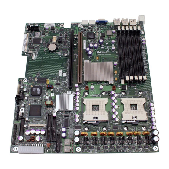
1U and 2U server markets. Server Board SE7520JR2 SKU Availability In this document, the name SE7520JR2 is used to describe the family of boards that are made available under a common product name. The core features for each board will be common;... - Page 22 Light-Guided Diagnostics on all FRU devices (processors, memory, power) • Port-80 Diagnostic LEDs displaying POST codes The following figure shows the board layout of the Server Board SE7520JR2. Each connector and major component is identified by number and is identified in Table 1. C78844-002...
-
Page 23: Figure 1. Se7520Jr2 Board Layout
Revision 1.0 Figure 1. SE7520JR2 Board Layout C78844-002... -
Page 24: Table 1: Baseboard Layout Reference
USB Port 1 Video Connector NIC #2 NIC #1 RJ-45 Serial B Port Stacked PS/2 Keyboard and Mouse Ports Intel Management Module Connector CMOS Battery Full Height Riser Card Slot Low Profile Riser Card Slot DIMM Slots 68-pin SCSI Channel A Connector LSI 53C1030 SCSI Controller MCH –... -
Page 25: Figure 2. Server Board Dimensions
Intel® Server Board SE7520JR2 Server Board Overview The following mechanical drawing shows the physical dimensions of the baseboard. Figure 2. Server Board Dimensions Revision 1.0 C78844-002... -
Page 26: Functional Architecture
This chapter provides a high-level description of the functionality associated with the architectural blocks that make up the Intel Server Board SE7520JR2. Note: This document describes the features and functionality of the Server Board SE7520JR2 when using standard on-board platform instrumentation. Some functionality and feature descriptions change when using either the Professional Edition or Advanced Edition Intel Management Modules. -
Page 27: Processor Sub-System
Flexible Mother Board (FMB) specification for all 800 MHz FSB Intel Xeon processors. FMB is an estimation of the maximum values the 800 MHz FSB versions of the Intel Xeon processors will have over their lifetime. The value is only an estimate and actual specifications for future processors may differ. -
Page 28: Common Enabling Kit (Cek) Design Support
® Note: Only Intel Xeon™ processors that support an 800MHz Front Side Bus are supported on the Server Board SE7520JR2. See the following table for a list of supported processors and their operating frequencies. Processor Family Intel® Xeon™... -
Page 29: Processor Mis-Population Detection
Processor Family Intel® Xeon™ Intel® Xeon™ Intel® Xeon™ 3.1.6.1 Processor Mis-population Detection The processors must be populated in the correct order for the processor front-side bus to be correctly terminated. CPU socket 1 must be populated before CPU socket 2. Baseboard logic will prevent the system from powering up if a single processor is present but it is not in the correct socket. -
Page 30: Microcode
3.1.6.7 Microcode IA-32 processors have the capability of correcting specific errata through the loading of an Intel- supplied data block (i.e., microcode update). The BIOS is responsible for storing the update in non-volatile memory and loading it into each processor during POST. The BIOS allows a number of microcode updates to be stored in the flash, limited by the amount of free space available. -
Page 31: Cpu Thermal Sensors
3.1.9 Processor Thermal Control Sensor The Intel Xeon processors generate a signal to indicate throttling due to a processor over temp condition. The mBMC implements an IPMI sensor that provides the percentage of time a processor has been throttled over the last 1.46 seconds. Baseboard management forces a thermal control condition when reliable system operation requires reduced power consumption. -
Page 32: Memory Controller Hub (Mch)
The following sub-sections provide an overview of the primary functions and supported features of each chipset component as they are used on the Server Board SE7520JR2. Later sections in this chapter provide more detail on the implementation of the sub-systems. -
Page 33: Hub Interface
For conventional PCI Mode, the PXH supports PCI bus frequencies of 66 MHz, 100 MHz, and 133 MHz. On the Server Board SE7520JR2 each of the two PCI-X interfaces (PCI Bus A and PCI Bus B) is independently controlled to operate in either a conventional PCI or PCI-X mode. PCI Bus A is... -
Page 34: I/Oxapic Controller
5-V tolerant, except PME#. The ICH5 integrates a PCI arbiter that supports up to six external PCI bus masters in addition to the internal ICH5 requests. On the Server Board SE7520JR2 this PCI interface is used to support on-board PCI devices including the ATI* video controller, Super I/O chip, and hardware monitoring sub-system. -
Page 35: Sata Controller
IDE channels of the ICH5R. One channel is accessed through the 40-pin connector on the baseboard. The signals of the second channel are routed to the 100-pin backplane connector for use in either the Intel Server Chassis SR1400 or SR2400 when integrated with a backplane for slim-line optical drive use. -
Page 36: Universal Serial Bus (Usb) Controller
USB 2.0 allows data transfers up to 480 Mb/s, which is 40 times faster than full-speed USB. The ICH5-R also contains four Universal Host Controller Interface (UHCI) controllers that support USB full-speed and low-speed signaling. On the Server Board SE7520JR2, the ICH5-R provides six USB 2.0 ports. All six ports are high-speed, full-speed, and low-speed capable. -
Page 37: Memory Sub-System
DIMM is a single load device, ie) Single Rank = 1 Load. Dual rank DIMMs are dual load devices, ie) Dual Rank = 2 loads. The Server Board SE7520JR2 provides the following maximum memory capacities based on the number of DIMM slots provided and maximum supported memory loads by the chipset: •... -
Page 38: Memory Population
For double-sided DIMMs, both rows are said to be present. The Server Board SE7520JR2 has six DIMM slots, or three DIMM banks. Both DIMMs in a bank should be identical (same manufacturer, CAS latency, number of rows, columns and devices, timing parameters etc.). -
Page 39: Table 3: Supported Ddr-266 Dimm Populations
Using the following algorithm, BIOS configures the memory controller of the MCH to run in either dual channel mode or single channel mode: (1) If 1 or more fully populated DIMM banks are detected, the memory controller is set to dual channel mode. -
Page 40: Ecc Memory Initialization
Table 5: Supported DDR2-400 DIMM Populations Bank 3 – DIMMs 3A, 3B Note: On the Server Board SE7520JR2, when using all dual rank DDR-333 or DDR2-400 DIMMs, a total of four DIMMs can be populated. Configuring more than four dual rank DDR- 333 or DDR2-400 DIMMs will result in the BIOS generating a memory configuration error. -
Page 41: Memory Monitoring
status of the extended memory test is displayed on the console. The status of base and extended memory tests are also displayed on an LCD control panel if present. The extended memory test is configured using the BIOS Setup Utility. The coverage of the test can be configured to one of the following: •... -
Page 42: Memory Rasum Features
3.3.6.2 Integrated Memory Scrub Engine The Intel E7520 MCH includes an integrated engine to walk the populated memory space proactively seeking out soft errors in the memory subsystem. In the case of a single bit correctable error, this hardware detects, logs, and corrects the data except when an incoming write to the same memory address is detected. -
Page 43: Retry On Uncorrectable Error
3.3.6.3 Retry on Uncorrectable Error The Intel E7520 MCH includes specialized hardware to resubmit a memory read request upon detection of an uncorrectable error. When a demand fetch (as opposed to a scrub) of memory encounters an uncorrectable error as determined by the enabled ECC algorithm, the memory control hardware will cause a (single) full resubmission of the entire cache line request from memory to verify the existence of corrupt data. -
Page 44: Dimm Sparing Function
3.3.6.5 DIMM Sparing Function To provide a more fault tolerant system, the Intel E7520 MCH includes specialized hardware to support fail-over to a spare DIMM device in the event that a primary DIMM in use exceeds a specified threshold of runtime errors. One of the DIMMs installed per channel, greater than or equal in size than all installed, will not be used but kept in reserve. -
Page 45: Memory Mirroring
Mirroring is supported on dual-channel DIMM populations symmetric both across channels and within each channel. As a result, on the Server Board SE7520JR2 there are two supported configurations for memory mirroring: •... -
Page 46: Figure 7. Six Dimm Memory Mirror Configuration (Ddr2 Only)
Figure 7. Six DIMM Memory Mirror Configuration (DDR2 Only) These symmetry requirements are a side effect of the hardware mechanism for maintaining two copies of all main memory data while ensuring that each channel has a full copy of all data in preparation for fail-down to single-channel operation. -
Page 47: Logging Memory Ras Information To The Sel
This section describes the function of each I/O interface and how they operate on the Server Board SE7520JR2. 3.4.1 PCI Subsystem The primary I/O interface for the Server Board SE7520JR2 is PCI, with four independent PCI bus segments. • A PCI 33MHz/32-bit bus segment (P32-A) is controlled through the ICH5-R. -
Page 48: P32-A: 32-Bit, 33-Mhz Pci Subsystem
3.4.1.4 PCI Riser Slots The Server Board SE7520JR2 has two riser slots capable of supporting riser cards for both 1U and 2U system configurations. Because of board placement resulting in different pin orientations, and expanded technology support associated with the full-height riser, the riser slots are proprietary and require different riser cards. -
Page 49: Pci Scan Order
8 PCI-Express card, or two x 4 PCI-Express cards. Intel makes available a 1U single slot x8 riser card and a 2U three slot riser card which provides two x8 connectors each supporting x4 data widths. The third slot is a PCI-X slot. Using a baseboard configured with an integrated SCSI controller, the PCI-X add-in slot is capable of supporting a bus speed of up to 100MHz. -
Page 50: Device Number And Idsel Mapping
Functional Architecture Intel® Server Board SE7520JR2 hierarchical PCI bus under the current bridge. The PCI bus number and the subordinate PCI bus number are the same in the last hierarchical bridge. 3.4.1.7 Device Number and IDSEL Mapping Each device under a PCI bridge has its IDSEL input connected to one bit out of the PCI bus address/data signals AD[31::11] for the PCI bus. -
Page 51: Table 8: Pci Configuration Ids And Device Numbers
LP Slot1 (64-bit, PCI-X-100) LP Slot2 (64-bit, PCI-X-100) LF Slot3 (64-bit, PCI-X-100) On board device Intel 82546GB(1Gb) NIC w/ dual channel LSI53C1030 Ultra 320 SCSI w/ dual channel ATI Rage XL (PCI VGA) Note: Bus Numbers may change depending on the type of riser card used. -
Page 52: Resource Assignment
The option ROM space is also used by the console redirection binary (if enabled) and the user binary (if present and configured for runtime usage). The SE7520JR2 BIOS integrates option ROMs for the Intel® 82546GB, the ATI* Rage XL, and the LSI* 53C1030 SCSI controller. -
Page 53: Apic Interrupt Routing
For APIC mode, the Server Board SE7520JR2 interrupt architecture incorporates three Intel I/O APIC devices to manage and broadcast interrupts to local APICs in each processor. The Intel I/O APICs monitor each interrupt on each PCI device including PCI slots in addition to the ISA compatibility interrupts IRQ(0-15). -
Page 54: Legacy Interrupt Sources
3.4.3.3 Legacy Interrupt Sources The table below recommends the logical interrupt mapping of interrupt sources on the Server Board SE7520JR2. The actual interrupt map is defined using configuration registers in the ICH5-R. Interrupt IRQ0 Timer/counter, HPET #0 in legacy replacement Mode. In APIC mode, cascade from 8259 controller #1... -
Page 55: Irq Scan For Pciirq
The IRQ / data frame structure includes the ability to handle up to 32 sampling channels with the standard implementation using the minimum 17 sampling channels. The Server Board SE7520JR2 has an external PCI interrupt serializer for PCIIRQ scan mechanism of ICH5-R to support 16 PCIIRQs. -
Page 56: Figure 9. Interrupt Routing Diagram
Super I/O Timer Keyboard Cascade Serial Serial Floppy/IS SCI/ISA Mouse/IS Coprocessor P_IDE/IS Not Used USB 1.1 Controller #1 and #4 Video USB 1.1 Controller #3, Native IDE and SATA USB 1.1 Controller #2 Option for SCI, TCO, HPET#0,1,2 Option for SCI, TCO, HPET#0,1,2 Option for SCI, TCO, HPET#0,1,2 USB 2.0 EHCI Controller #1, Option for SCI, TCO, HPET#0,1,2... -
Page 57: Figure 10. Pci Interrupt Mapping Diagram
Intel® Server Board SE7520JR2 Functional Architecture Figure 10. PCI Interrupt Mapping Diagram Figure 11. PCI Interrupt Mapping Diagram for 2U Active Riser Card Revision 1.0 C78844-002... -
Page 58: Scsi Support
3.4.4 SCSI Support The SCSI sub-system consists of the LSI 53C1030 Dual Channel Ultra320 SCSI controller, one internal 80-pin connector (SCSI Channel A), one external high 80-pin density SCSI connector (SCSI channel B), and on-board termination for both SCSI channels. 3.4.4.1 LSI* 53C1030 Dual Channel Ultra320 SCSI Controller The LSI53C1030 is a PCI-X to Dual Channel Ultra320 SCSI Multifunction Controller that... - Page 59 • Quick arbitrate and select (QAS) • Skew compensation • Inter-symbol interference (ISI) compensation • Cyclic redundancy check (CRC) • Domain validation technology The LSI53C1030 contains the following SCSI performance features: • Supports Ultra320 SCSI • Paced transfers using a free running clock •...
-
Page 60: Zero Channel Raid
RUBI2 standard. It will not have support for zero channel RAID cards that follow the RADIOS standard. See the SE7520JR2 Tested Hardware and OS list for a list of supported ZCR cards. Zero channel RAID (ZCR) capabilities enable the LSI 53C1030 to respond to accesses from a PCI RAID controller card or chip that is able to generate ZCR cycles. -
Page 61: Ultra Ata/100
The BIOS initializes and supports ATAPI devices such as LS-120/240, CDROM, CD-RW and DVD. The BIOS initializes and supports S-ATA devices just like P-ATA devices. It initializes the embedded the IDE controllers in the chipset and any S-ATA devices that are connected to these controllers. -
Page 62: Sata Raid
The Intel RAID Technology for SATA Option ROM provides a pre-OS user interface for the Intel RAID Technology implementation and provides the ability for an Intel RAID Technology volume to be used as a boot disk as well as to detect any faults in the Intel RAID Technology volume(s) attached to the Intel RAID controller. -
Page 63: Video Memory Interface
Requests are serviced in a manner that ensures display integrity and maximum CPU/coprocessor drawing performance. The Server Board SE7520JR2 supports an 8MB (512Kx32bitx4 Banks) SDRAM device for video memory. The following table shows the video memory interface signals:... -
Page 64: Dual Video
3.4.8 Network Interface Controller (NIC) The Intel 82546GB dual-channel gigabit network interface controller supplies the baseboard with two network interfaces. The 82546GB is a highly integrated PCI LAN controller in a 21 mm PBGA package. Each channel is capable of supporting 10/100/1000 operation and alert-on-LAN functionality. -
Page 65: Nic Connector And Status Leds
• Wake up control 3.4.10.1 GPIOs The National Semiconductor* PC87427 Super I/O provides nine general-purpose input/output pins that the Server Board SE7520JR2 utilizes. The following table identifies the pin and the signal name used in the schematic: GPIO00/CLKRUN_L GPIO01/KBCLK GPIO02/KBDAT... - Page 66 XBUS_A<4> XBUS_XRD_L XBUS_XWR_L XBUS_A<3> XBUS_A<2> XBUS_A<1> XBUS_A<0> XBUS_XCS0_L XBUS_D<7> XBUS_D<6> XBUS_D<5> XBUS_D<4> XBUS_D<3> XBUS_D<2> XBUS_D<1> XBUS_D<0> I/O,I(E)1 I/O,I(E)1 I/O,I(E)1 I/O,I(E)1 ZZ_POST_CLK_LED_L I/O,I(E)1 ZZ_BIOS_ROLLING I/O,I(E)1 FP_PWR_LED_L I/O,I(E)1 I/O,I(E)1 SIO_PME_L ZZ_POST_DATA_LED_L CLK_48M_SIO PU_XBUS_XCNF2 XBUS_XSTB1_L PU_XBUS_XCNF0 PU_SIO_ACBSA PU_SIO_CKIN48 C78844-002 SE7520JR2 Use Revision 1.0...
-
Page 67: Serial Ports
3.4.10.2.3 Serial Port Multiplexer Logic The Server Board SE7520JR2 has a multiplexer to connect the rear RJ45 connector to either Serial Port A or Serial Port B. This facilitates the routing of Serial Port A to the rear RJ45 connector if Serial Port B is used for Serial Over LAN (SOL). This serial port selection can be done through the BIOS setup option. -
Page 68: Figure 12. Serial Port Mux Logic
Serial B Serial A 3.4.10.2.4 Rear RJ45 Serial B Port Configuration The rear RJ45 Serial B port is a fully functional serial port that can support any standard serial device. Using an RJ45 connector for a serial port gives direct support for serial port concentrators, which are widely used in the high-density server market. -
Page 69: Removable Media Drives
2MB programmable. The flash ROM contains system initialization routines, setup utility, and runtime support routines. The exact layout is subject to change, as determined by Intel. A 128- KB block is available for storing OEM code (user binary) and custom logos. -
Page 70: Configuration And Initialization
3.5.1 Memory Space At the highest level, the Intel Xeon processor address space is divided into four regions, as shown in the following figure. Each region contains the sub-regions that are described in following sections. Attributes can be independently assigned to regions and sub-regions using registers. -
Page 71: Dos Compatibility Region
3.5.1.1 DOS Compatibility Region The first region of memory below 1 MB was defined for early PCs, and must be maintained for compatibility reasons. The region is divided into sub-regions as shown in the following figure. 0FFFFFh System BIOS 0F0000h 0EFFFFh Extended System BIOS... - Page 72 3.5.1.1.1 DOS Area The DOS region is 512 KB in the address range 0 to 07FFFFh. This region is fixed and all accesses go to main memory. 3.5.1.1.2 ISA Window Memory The ISA Window Memory is 128 KB between the address of 080000h to 09FFFFh. This area can be mapped to the PCI bus or main memory.
-
Page 73: Extended Memory
3.5.1.2 Extended Memory Extended memory is defined as all address space greater than 1MB. Extended Memory region covers 8GB maximum of address space from addresses 0100000h to FFFFFFFh, as shown in the following figure. PCI memory space can be remapped to top of memory (TOM). Extended lntel E7520 chipset region... -
Page 74: Memory Shadowing
3.5.1.2.1 Main Memory All installed memory greater than 1MB is mapped to local main memory, up to 8GB of physical memory. Memory between 1MB to 15MB is considered to be standard ISA extended memory. 1MB of memory starting at 15MB can be optionally mapped to the PCI bus memory space. The remainder of this space, up to 8GB, is always mapped to main memory, unless TBSG SMM is used which is just under TOLM. -
Page 75: System Management Mode Handling
System Management RAM (SMRAM) provides code and data storage space for the SMI_L handler code, and is made visible to the processor only on entry to SMM, or other conditions that can be configured using Intel Lindenhurst PF chipset. The MCH supports three SMM options: •... -
Page 76: I/O Map
PC-compatible I/O devices and functions, which are mapped to specific addresses in I/O space. On SE7520JR2, the ICH5-R provides the bridge to ISA functions. The I/O map in the following table shows the location in I/O space of all direct I/O-accessible registers. - Page 77 Address (es) 0071h RTC Data 0073h RTC Data 0075h RTC Data 0077h RTC Data 0080h – 0081h BIOS Timer 0080h – 008F DMA Low Page Register 0090h – 0091h DMA Low Page Register (aliased) 0092h System Control Port A (PC-AT control Port) (this port not aliased in DMA range) 0093h –...
-
Page 78: Accessing Configuration Space
Parallel Port (ECP) 07BCh – 07Beh Parallel Port (ECP) 0CF8h PCI CONFIG_ADDRESS Register 0CF9h Intel® Server Board SE7520JR2 Turbo and Reset Control 0CFCh PCI CONFIG_DATA Register 3.5.3 Accessing Configuration Space All PCI devices contain PCI configuration space, accessed using mechanism #1 defined in the PCI Local Bus Specification. -
Page 79: Config_Address Register
3.5.3.1 CONFIG_ADDRESS Register CONFIG_ADDRESS is 32 bits wide and contains the field format shown in the following figure. Bits [23::16] choose a specific bus in the system. Bits [15::11] choose a specific device on the selected bus. Bits [10:8] choose a specific function in a multi-function device. Bit [7::1] select a specific register in the configuration space of the selected device or function on the bus. -
Page 80: System Bios
IA-32 Core – The IA-32 core contains standard services and components such as the PCI Resource manager, ACPI support, POST, and runtime functionality. • Manageability Extensions – Intel servers build server management into the BIOS through the Intelligent Platform Management Interface (IPMI) and baseboard management hardware. -
Page 81: Flash Architecture And Flash Update Utility
The flash ROM contains system initialization routines, the BIOS Setup Utility, and runtime support routines. The exact layout is subject to change, as determined by Intel. A 64-KB user block is available for user ROM code or custom logos. The flash ROM also contains initialization code in compressed form for onboard peripherals, like SCSI, NIC and video controllers. -
Page 82: System Activity Window
4.3.1.1 System Activity Window The top row of the screen is reserved for the system state window. On a graphics console, the window is 640x48. On a text console, the window is 80x2. The system state window may be in one of three forms, either an activity bar that scrolls while the system is busy, a progress bar that measures percent complete for the current task, or an attention required bar. -
Page 83: Post Activity Window
<Esc> key while in Quiet Boot mode. If Quiet Boot is disabled, the BIOS displays diagnostic messages in place of the activity indicator and the splash screen. With the use of an Intel supplied utility, the BIOS allows OEMs to override the standard Intel logo with one of their own design 4.3.1.3... -
Page 84: Bios Setup Utility
Please select boot device: Floppy Hard Drives ATAPI CDROM LAN PXE EFI Boot Manager ↓and↑ to move selection Enter to select boot device ESC to boot using defaults BIOS Setup Utility The BIOS Setup utility is provided to perform system configuration changes and to display current settings and environment information. -
Page 85: Entering Bios Setup
Option ↔ Select Menu The left and right arrow keys are used to move between the major menu pages. The keys have no affect if a sub-menu or pick list is displayed. Select Field The Tab key is used to move between fields. For example, Tab can be used to move from hours to minutes in the time item in the main menu. -
Page 86: Advanced Menu
Feature Options System Overview AMI BIOS Version Build Date Processor Type Speed Count System Memory Size System Time HH:MM:SS System Date DAY MM/DD/YYYY Language English French German Italian Spanish 4.4.2.2 Advanced Menu Table 20: BIOS Setup, Advanced Menu Options Feature Options Advanced Settings WARNING: Setting wrong values in below sections may cause system to malfunction. -
Page 87: Table 21: Bios Setup, Processor Configuration Sub-Menu Options
Disabled Enabled Max CPUID Value Limit Disabled Enabled Hyper-Threading Technology Disabled Enabled Intel ® Speed Step ™ Tech Auto Disabled Revision 1.0 Options Help Text If enabled, all processors will be activated and retested on the next boot. This option will be automatically reset to disabled on the next boot. -
Page 88: Ide Configuration Submenu
4.4.2.2.2 IDE Configuration Sub-menu Table 22: BIOS Setup IDE Configuration Menu Options Feature Options IDE Configuration Onboard P-ATA Disabled Channels Primary Secondary Both Onboard S-ATA Disabled Channels Enabled Configure S-ATA as Disabled RAID Enabled S-ATA Ports A1-3 M/A2-4 Definition A1-4 M/A2-3 Mixed P-ATA / S-ATA N/A Primary IDE Master... -
Page 89: Table 23: Mixed P-Ata-S-Ata Configuration With Only Primary P-Ata
Feature Options Third IDE Master Fourth IDE Master Hard Disk Write Disabled Protect Enabled IDE Detect Time Out (Sec) ATA(PI) 80Pin Cable Host & Device Detection Host Device Table 23: Mixed P-ATA-S-ATA Configuration with only Primary P-ATA Feature Options Mixed P-ATA / S-ATA First ATA P-ATA M-S Channel... -
Page 90: Table 24: Bios Setup, Ide Device Configuration Sub-Menu Selections
Table 24: BIOS Setup, IDE Device Configuration Sub-menu Selections Feature Options Primary/Secondary/Third/Fourth IDE Master/Slave Device Vendor Size LBA Mode Block Mode PIO Mode Async DMA Ultra DMA S.M.A.R.T. Type Not Installed Auto CDROM ARMD LBA/Large Mode Disabled Auto Block (Multi-Sector Disabled Transfer) Mode Auto... -
Page 91: Table 25: Bios Setup, Floppy Configuration Sub-Menu Selections
Allows BIOS to Select Serial Port A Base Addresses. Allows BIOS to Select Serial Port B Base Addresses. C78844-002 Description Note: Intel no longer validates 720Kb & 2.88Mb drives. Description Option that is used by other serial port is hidden to prevent conflicting settings. -
Page 92: Table 27: Bios Setup, Usb Configuration Sub-Menu Selections
4.4.2.2.5 USB Configuration Sub-menu Table 27: BIOS Setup, USB Configuration Sub-menu Selections Feature Options USB Configuration USB Devices Enabled USB Function Disabled Enabled Legacy USB Support Disabled Keyboard only Auto Keyboard and Mouse Port 60/64 Emulation Disabled Enabled USB 2.0 Controller Disabled Enabled USB 2.0 Controller... -
Page 93: Table 29: Bios Setup, Pci Configuration Sub-Menu Selections
Feature Options Device #n Emulation Type Auto Floppy Forced FDD Hard Disk CDROM 4.4.2.2.6 PCI Configuration Sub-menu This sub-menu provides control over PCI devices and their option ROMs. If the BIOS is reporting POST error 146, use this menu to disable option ROMs that are not required to boot the system. -
Page 94: Table 30: Bios Setup, Memory Configuration Sub-Menu Selections
Feature Options Slot 1 Option ROM Disabled Enabled Slot 2 Option ROM Disabled Enabled Slot 3 Option ROM Disabled Enabled Slot 4 Option ROM Disabled Enabled Slot 5 Option ROM Disabled Enabled Slot 6 Option ROM Disabled Enabled 4.4.2.2.7 Memory Configuration Sub-menu This sub-menu provides information about the DIMMs detected by the BIOS. -
Page 95: Boot Menu
Feature Options DIMM 3A Installed Not Installed Disabled Mirror Spare DIMM 3B Installed Not Installed Disabled Mirror Spare Extended Memory Test 1 MB 1 KB Every Location Disabled Memory Retest Disabled Enabled Memory Remap Feature Disabled Enabled Memory Mirroring / Sparing Disabled Spare Mirror... -
Page 96: Table 32: Bios Setup, Boot Settings Configuration Sub-Menu Selections
4.4.2.3.1 Boot Settings Configuration Sub-menu Selections Table 32: BIOS Setup, Boot Settings Configuration Sub-menu Selections Feature Options Boot Settings Configuration Quick Boot Disabled Enabled Quiet Boot Disabled Enabled (this is conflict with previous words in this doc. Based on my memory, it is enabled by default) -
Page 97: Table 33: Bios Setup, Boot Device Priority Sub-Menu Selections
4.4.2.3.2 Boot Device Priority Sub-menu Selections Table 33: BIOS Setup, Boot Device Priority Sub-menu Selections Feature Options Boot Device Priority 1st Boot Device Varies Specifies the boot sequence from the available devices. A device enclosed in parenthesis has been disabled in the corresponding type menu. -
Page 98: Security Menu
nth Drive Varies Specifies the boot sequence from the available devices. 4.4.2.4 Security Menu Table 37: BIOS Setup, Security Menu Options Feature Options Security Settings Administrator Password is User Password is Set Admin Password Set User Password User Access Level No Access View Only Limited... -
Page 99: Server Menu
This node is grayed out if a user password is not installed. This node is grayed out if a user password is not installed. This node is hidden if the Intel Management Module is not present. This node is grayed out if a user password is not installed. -
Page 100: Table 39: Bios Setup, System Management Sub-Menu Selections
Feature Late POST Timeout Disabled 5 minutes 10 minutes 15 minutes 20 minutes Hard Disk OS Boot Timeout Disabled 5 minutes 10 minutes 15 minutes 20 minutes PXE OS Boot Timeout Disabled 5 minutes 10 minutes 15 minutes 20 minutes OS Watchdog Timer Policy Stay On Reset... -
Page 101: Table 40: Bios Setup, Serial Console Features Sub-Menu Selections
B selects UARTB. Help Text Setting this to Enabled will clear the System Event Log during the next boot. C78844-002 Description When the Intel Management Module is present, the help text directs the user to select Serial B for Serial Over LAN. -
Page 102: Exit Menu
Feature Options BIOS Event Logging Disabled Enabled Critical Event Logging Disabled Enabled ECC Event Logging Disabled Enabled PCI Error Logging Disabled Enabled FSB Error Logging Disabled Enabled Hublink Error Logging Disabled Enabled 4.4.2.6 Exit Menu Table 42: BIOS Setup, Exit Menu Selections Feature Options Exit Options... -
Page 103: Flash Update Utility
The active partition from which the system boots shall be referred to as the primary partition. The AMI FLASH update suite and Intel Online updates preserve the existing BIOS image on the primary partition. BIOS updates are diverted to the secondary partition. After the update is complete, a notification flag is set. -
Page 104: Bios Recovery
When a request is detected, the BIOS loads the default system configuration values during the next POST. In systems configured with an Intel Management Module, the CMOS can be cleared without opening the chassis. Using the control panel, the user can hold the reset button for 4 seconds and then press the power button while still pressing the reset button. -
Page 105: Oem Binary
System software can locate a run-time user binary by searching for it like an option ROM. The system vendor can place a signature within the user binary to distinguish it from other option ROMs. Refer to the SE7520JR2 BIOS EPS for further details. -
Page 106: Operating Model
Operating Model The following table summarizes the operation of security features supported by the BIOS. Some security features require the Intel Management Module (IMM) to be installed. These include “Diskette Write Protect”, “Video Blanking”, and “Power Switch inhibit.” Table 43: Security Features Operating Model... - Page 107 Administrator/User Passwords and F2 Setup Usage Model Notes: • Visible=option string is active and changeable • Hidden=option string is inactive and not visible • Shaded=option string is gray-out and view-only There are three possible password scenarios: Scenario #1 Administrator Password Is Not Installed User Password Is Not Installed...
-
Page 108: Password Clear Jumper
Get System Boot Options Command, takes appropriate action, and clears these settings. 4.9.1 Microsoft* Windows* Compatibility Intel Corporation and Microsoft Corporation co-author design guides for system designers using ® Intel processors and Microsoft* operating systems. These documents are updated yearly to address new requirements and current trends. -
Page 109: Advanced Configuration And Power Interface (Acpi)
Intel® Server Board SE7520JR2 System BIOS PC200x specifications are intended for systems that are designed to work with Windows 2000* and Windows XP* class operating systems. The Hardware Design Guide (HDG) for the Windows XP platform is intended for systems that are designed to work with Windows XP class operating systems. -
Page 110: Power Switch Off To On
The BIOS supports a control panel sleep button. The sleep button may not be provided on all control panel designs. On systems where the sleep button is optional, a system configuration option will be provided to enable or disable the sleep button. The ACPI tables will be updated to indicate the presence or absence of the sleep button. -
Page 111: Sleep To On (Acpi)
4.9.2.6 Sleep to On (ACPI) If an operating system is loaded, the sleep button generates a wake event to the ACPI chipset and a request (via SCI) to the OS to place the system in the “On” state. The OS retains control of the system and OS policy determines what sleep state (if any) and sleep sources the system can wake from. -
Page 112: 4.10 Pxe Bios Support
4.10 PXE BIOS Support The BIOS will support PXE-compliant implementations that: • Locate and configure all PXE-capable boot devices (UNDI Option ROMs) in the system, both built-in and add-ins. • Supply a PXE according to the specification if the system includes a built-in network device. •... -
Page 113: Platform Management
IPMB. Through the redirection capabilities of the BMC on Intel® platforms, this serial port UART input/output stream is further redirected and sent over a platform LAN device as a packetized serial-byte stream. This BMC function is called Serial over LAN, or SOL, and further optimizes space requirements and server management capability. - Page 114 Sahalee BMC. If a described feature or function is unique, the specific management controller will be referenced. On-Board Platform Instrumentation Limited Limited Errors Only C78844-002 Intel® Intel® Management Management Module - Module - Professional Advanced Edition Edition Revision 1.0...
-
Page 115: Platform Management Architecture Overview
Platform Management Architecture Overview LM 93 ProcHot VID_CPU0[5:0] P1_VID[5:0] VID_CPU1[5:0] ThermTrip P2_VID[5:0] Not Used +12V1 P12V_CPU_SCALED +12V2 IERR P12V_SCALED +12V3 P_VTT FSB_Vtt P1V5 Chipset_Core Not Used ICH_Core P_VCCP0 Zone 1 CPU1_Vccp P_VCCP1 PWM1 CPU2_Vccp P3V3 3.3V Zone2 P1V8_SCSI PWM2 SCSI_Core DDR Core Mem_Core DDR Vtt... -
Page 116: Standby
5.1.1 5V Standby The power supply must provide a 5V Standby power source for the platform to provide any management functionality. 5V Standby is a low power 5V supply that is active whenever the system is plugged into AC power. 5V Standby is used by the following onboard management devices: •... -
Page 117: Ipmi 'Sensor Model
Intel® Server Board SE7520JR2 Platform Management 5.1.3 IPMI ‘Sensor Model’ An IPMI-compatible ‘Sensor Model’ is used to unify the way that temperature, voltage, and other platform management status and control is represented and accessed. The implementation of this model is done according to command and data formats defined in the Intelligent Platform Management Interface Specification. -
Page 118: Private Management Busses
Management Controllers At the heart of platform management is a management controller. To support the tiered management model, the Server Board SE7520JR2 supports two different management controllers, the PC87431M mini-Baseboard Management Controller (mBMC) from National Semiconductor* and Intel’s Sahalee BMC. The Professional and Advanced modules electrically replace the mBMC with the more full featured ‘Sahalee’... - Page 119 • FRU Information Access. FRU (Field Replaceable Unit) information is non-volatile storage for serial number, part number, asset tag and other inventory information for the baseboard and chassis. The FRU implementation on SE7520JR2 includes write support for OEM-specific records. •...
- Page 120 • Platform Event Filtering (PEF) • Keyboard Controller Style (KCS) IPMI-System Interface (Professional and Advanced systems only) • SMBus IPMI-System Interface (On-board Platform Instrumentation systems only) • Intelligent Chassis Management Bus (ICMB) support (Professional and Advanced systems only) • Remote Boot Control •...
-
Page 121: On-Board Platform Management Features And Functionality
Intel® Server Board SE7520JR2 Platform Management On-Board Platform Management Features and Functionality The National Semiconductor PC87431M mini-Baseboard Management Controller (mBMC) is an Application Specific Integrated Circuit (ASIC) with a Reduced Instruction Set Computer (RISC)- based processor and many peripheral devices embedded into it. It is targeted for a wide range of remote-controlled platforms, such as servers, workstations, hubs, and printers. -
Page 122: Server Management I C Buses
5.2.1 Server Management I The table below describes the server management I that are connected to the indicated bus. The column labeled “I physical I C bus connected to the mBMC. Only the Peripheral SMBus is available for use with the Write-Read I C IPMI command. -
Page 123: Mbmc Hardware Architecture
Intel® Server Board SE7520JR2 Platform Management Figure 21. External Interfaces to mBMC mBMC Hardware Architecture The following figure shows an example of the internal functional modules of the mBMC in a block diagram. The mBMC controls various server management functions, such as the system power/reset control, a variety of types of sensor monitoring, system initialization, fault resilient booting (FRB). -
Page 124: Power Supply Interface Signals
Platform Management Intel® Server Board SE7520JR2 Figure 22. mBMC Block Diagram 5.3.1 Power Supply Interface Signals The mBMC supports two power supply control signals: Power On and Power Good. The Power On signal connects to the chassis power subsystem through the chipset and is used to request power state changes (asserted = request Power On). -
Page 125: Figure 23. Power Supply Control Signals
The following figure shows the power supply control signals and their sources. To turn on the system, the mBMC asserts the Power On signal and waits for the Power Good signal to assert in response, indicating that DC power is on. Figure 23. -
Page 126: Power Control Sources
5.3.2 Power Control Sources The sources listed in the following table can initiate power-up and/or power-down activity. Source Power button Front control power button mBMC Watchdog Timer Internal mBMC timer Platform Event Filtering Command Routed through command processor Power state retention Implemented via mBMC internal logic 5.3.3 Power-up Sequence... -
Page 127: Reset Control Sources
RSTOUT output if Control Panel Lockout is disabled. The “Control Panel Reset Button pressed” event is logged in the SEL. The Intel® Local Control Panel with LCD, is not supported with on-board platform management. Either an IMM Professional Editaion or Advanced Edition must be installed to support this chassis option. -
Page 128: Control Panel Indicators
• Combined power and reset button assertion If DC power is off, an assertion of the PWBTIN while the RSTIN is asserted generates an OEM-specific Control Panel event to PEF. The event attributes are: Sensor Type code - 14h (Button) and Sensor Specific offset - 07h. This PEF action initiates a BIOS CMOS clear request to the system BIOS. -
Page 129: Control Panel Inputs
5.3.5.4.2 Fault / Status LED The following table shows mapping of sensors/faults to the LED state. Color Condition Solid System ready Green Blink System ready, but degraded: CPU disabled Solid Critical failure: critical fan, voltage, or temperature state Amber Blink Non-critical failure: non-critical fan, voltage, or temperature state Solid System not ready: POST error / NMI event / CPU or terminator missing... -
Page 130: Chassis Intrusion
5.3.5.5.1 Chassis Intrusion Some platforms support chassis intrusion detection. On those platforms, the mBMC monitors chassis intrusion by polling the server input/output (SIO) device. The state of the chassis intrusion input is provided by the status register of the SIO device. A Chassis Intrusion event is logged in the System Event Log when a change in the input state is detected. -
Page 131: Secure Mode Operation
The mBMC supports a maximum SEL size of 92 entries. If an Intel® Management Module is installed in the server, the mBMC System Event Log is not accessible and is replaced by the Intel Management Module System Event Log. -
Page 132: Sel Erasure
The mBMC supports both low-going and high-going sensor devices. If an Intel Management Module is installed in the server, the mBMC SDRs are not accessible and are replaced by the Intel Management Module SDRs. -
Page 133: Field Replaceable Unit (Fru) Inventory Devices
5.3.12 Field Replaceable Unit (FRU) Inventory Devices An enterprise-class system typically has FRU information for each major system board, (processor board, memory board, I/O board, etc.). The FRU data includes information such as serial number, part number, model, and asset tag. This information can be accessed in two ways: through IPMI FRU commands or by using Master Write-Read commands. -
Page 134: Mbmc Self Test
5.3.16 mBMC Self Test The mBMC performs various tests as part of its initialization. If a failure is determined (e.g., corrupt mBMC FRU, SDR, or SEL), the mBMC stores the error internally. 5.3.17 Messaging Interfaces This section describes the supported mBMC communication interfaces: •... -
Page 135: Lan Interface
• SMBus data signal (SDAH) • Optional SMBus alert signal (SMBAH). The signal notifies the host that the PC87431x has data to provide. When the system main power is off (PWRGD signal is low), the host interface signals are in TRI-STATE to perform “passive”... -
Page 136: Event Filtering And Alerting
LAN Channel Capability Privilege Levels Authentication Types Number of LAN Alert Destinations Address Resolution Protocol (ARP) 5.3.18 Event Filtering and Alerting The mBMC implements most of the IPMI 1.5 alerting features. The following features are supported: • • Alert over LAN 5.3.18.1 Platform Event Filtering (PEF) The mBMC monitors platform health and logs failure events into the SEL. -
Page 137: Alert Over Lan
down, power cycle, and/or reset actions, the actions are performed according to PEF Action Priorities. Note: An action that has changed from delayed to non-delayed, or an action whose delay time has been reduced automatically has higher priority. The mBMC can be configured to log PEF actions as SEL events. -
Page 138: Table 55: Platform Sensors For On-Board Platform Instrumentation
mBMC sensors 01h – 08h are internal sensors to the mBMC and are used for event generation only. These sensors are not for use with the ‘Get Sensor Reading’ IPMI command and may return an error when read. Table 55: Platform Sensors for On-Board Platform Instrumentation Sensor Name Sensor Type Physical... - Page 139 Intel® Server Board SE7520JR2 Sensor Sensor Name Type Physical Physical Security Security Violation Voltage CPU1 12v Voltage CPU2 12v Voltage BB +1.5V Voltage BB +1.8V Voltage BB +3.3V Voltage BB +5V Voltage BB +12V Voltage BB -12V Voltage FSB Vtt...
- Page 140 As & De Threshold [u,l][ c,nc] As & De Threshold [u,l][ c,nc] As & De Generic State Asserted As & De C78844-002 Intel® Server Board SE7520JR2 Readable Event Data Value/Offsets Action Fault LED Analog R, T Action Fault LED Analog...
- Page 141 Intel® Server Board SE7520JR2 Platform Management Revision 1.0 C78844-002...
-
Page 142: Imm Bmc Sensor Support
The following tables are for the built-in and the external sensors for the platform when either an Intel Management Module Professional or Advanced is installed. Table 56. Platform Sensors for Intel Management Modules - Professional and Advanced Sensor Sensor Name... - Page 143 Intel® Server Board SE7520JR2 Sensor Sensor Name Sensor Type Number Critical Inerrupt Critical Interrupt Sensor Memory Memory Event Logging Event Logging Disabled Disabled Session Audit Session Audit Voltage BB +1.2V Vtt BB+1.2V Voltage NIC Core Voltage BB +1.5V BB +1.8V...
- Page 144 Lags Digital Performance Met Discrete As & De or Lags Digital Performance Met Discrete As & De or Lags C78844-002 Intel® Server Board SE7520JR2 Readable Value / EventData Offsets Analog R, T Analog R, T Analog R, T Analog...
- Page 145 Intel® Server Board SE7520JR2 Sensor Sensor Name Sensor Type Number Digital Fan 10 Digital Fan 11 LVDS SCSI Terminator channel 1 terminator fault LVDS SCSI Terminator channel 2 terminator fault Power Supply Power Supply Status 1 Power Supply Power Supply...
- Page 146 Specific Entity Present IERR Thermal Trip FRB1, FRB2, Sensor FRB3 Specific As & De Config Error Presence Disabled C78844-002 Intel® Server Board SE7520JR2 Readable Value / EventData Offsets – Trig Offset – Trig Offset – Trig Offset – Trig Offset –...
- Page 147 Intel® Server Board SE7520JR2 Sensor Sensor Name Sensor Type Number Processor 2 Processor Status Processor 1 Core Temp Temp Processor 2 Core Temp Temp Processor 1 12v Voltage Processor 2 12v Voltage Processor 1 Temp Thermal Control Processor 2 Temp...
-
Page 148: Wired For Management (Wfm)
Using SMBIOS, a system administrator can obtain the types, capabilities, operational status, installation date and other information about the system components. Refer to the SE7520JR2 BIOS EPS for detail describing access methods to the SMBIOS structure tables. Event /... -
Page 149: Error Reporting And Handling
IPMI watchdog timer to protect against BIOS hangs during the POST process On systems that have an Intel Management Module installed, several different levels of FRB are supported: FRB1, FRB2, FRB3, and OS Watchdog Timer. The FRB algorithms detect BSP failures and take steps to disable that processor and reset the system so another processor will run as the BSP. -
Page 150: Frb3 - Bsp Reset Failures
The first timer (FRB3) starts counting down whenever the system comes out of hard reset. With no Intel® Management Module, only one watchdog timer is present. If the BSP successfully resets and begins executing, the BIOS disables the FRB-3 timer in the BMC and the system continues executing POST. -
Page 151: Ap Failures
6.1.5 AP Failures In systems configured with an Intel Management Module, the BIOS and Sahalee BMC implement additional safeguards to detect and disable the application processors (AP) in a multiprocessor system. If an AP fails to complete initialization within a certain time, it is assumed to be nonfunctional. -
Page 152: Memory Error Handling In Ras Mode
does not alter the BSP and attempts to boot from the original BSP. Error messages are displayed on the console, and errors are logged in the event log of a processor failure. If the user replaces a processor that has been marked bad by the system, the system must be informed about this change by running BIOS Setup and selecting that processor to be retested. -
Page 153: Memory Error Handling In Non-Ras Mode
The following table shows memory error handling with both a mBMC and Sahalee BMC. Table 57: Memory Error Handling mBMC vs Sahalee Memory with RAS Server with mBMC mode Sparing mode / When Sparing or Mirroring occurs: Mirroring mode - BIOS will not report memory RAS configuration to mBMC. -
Page 154: Dimm Enabling
In non-RAS mode, BIOS will assert a Non-Maskable-Interrupt (NMI) on the first Double Bit ECC (DBE) error. Table 58: Memory Error Handling in non-RAS mode Non-RAS mode Server with mBMC Single Bit ECC SBE error events will not be (SBE) errors logged. -
Page 155: Error Logging
Error Logging This section defines how errors are handled by the system BIOS. Also discussed is the role of the BIOS in error handling and the interaction between the BIOS, platform hardware, and server management firmware with regard to error handling. In addition, error-logging techniques are described and beep codes for errors are defined. -
Page 156: Memory Bus Error
6.3.4 Memory Bus Error The hardware is programmed to generate an SMI on single-bit data errors in the memory array if ECC memory is installed. The SMI handler records the error and the DIMM location to the system event log. Double-bit errors in the memory array are mapped to the SMI because the mBMC cannot determine the location of the bad DIMM. -
Page 157: Table 60: Boot Bios Messages
Gate20 Error Multi-Bit ECC Error Parity Error Message Displayed Boot Failure ... Invalid Boot Diskette Drive Not Ready A: Drive Error B: Drive Error Insert BOOT diskette in A: Reboot and Select proper Boot device or Insert Boot Media in selected Boot device NO ROM BASIC Table 61: Storage Device BIOS Messages Message Displayed... - Page 158 Message Displayed Primary Slave Hard Disk Error Secondary Master Hard Disk Error Secondary Slave Hard Disk Error Master Hard Disk Error Slave Hard Disk Error Master Hard Disk Error Slave Hard Disk Error Master Hard Disk Error Slave Hard Disk Error Master Hard Disk Error Slave Hard Disk Error Primary Master Drive - ATAPI Incompatible...
- Page 159 Message Displayed Secondary Master Drive - ATAPI Incompatible Secondary Slave Drive - ATAPI Incompatible Master Drive - ATAPI Incompatible Slave Drive - ATAPI Incompatible Master Drive - ATAPI Incompatible Slave Drive - ATAPI Incompatible Master Drive - ATAPI Incompatible Slave Drive - ATAPI Incompatible Master Drive - ATAPI Incompatible Slave Drive - ATAPI Incompatible S.M.A.R.T.
-
Page 160: Table 62: Virus Related Bios Messages
EPROM). BIOS could not find or load the CPU Microcode Update to the CPU. This message only applies to INTEL CPUs. The message is most likely to appear when a brand new CPU is installed in a motherboard with an outdated BIOS. -
Page 161: Table 64: Cmos Bios Messages
Message Displayed Interrupt Controller-1 error Interrupt Controller-2 error Message Displayed CMOS Date/Time Not Set CMOS Battery Low CMOS Settings Wrong CMOS Checksum Bad Table 65: Miscellaneous BIOS Messages Message Displayed Keyboard Error PS2 Keyboard not found PS2 Mouse not found Keyboard/Interface Error Unlock Keyboard System Halted... -
Page 162: Post Error Codes
Halt: The message is displayed on the screen, an error is logged to the SEL, and the system cannot boot unless the error is corrected. The error codes are defined by Intel and whenever possible are backward compatible with error codes used on earlier platforms. - Page 163 Error Code 0012 CMOS time not set 0014 PS2 Mouse not found 0040 Refresh timer test failed 0041 Display memory test failed 0042 CMOS Display Type Wrong 0043 ~<INS> Pressed 0044 DMA Controller Error 0045 DMA-1 Error 0046 DMA-2 Error 0047 Unknown BIOS error.
-
Page 164: Table 69: Error Codes Sent To The Management Module
Error Code 8130 Processor 01 disabled 8131 Processor 02 disabled 8140 Processor 01 failed FRB-3 timer 8141 Processor 02 failed FRB-3 timer 8150 Processor 01 failed initialization on last boot. 8151 Processor 02 failed initialization on last boot. 8160 Processor 01 unable to apply BIOS update 8161 Processor 02 unable to apply BIOS update 8170... -
Page 165: Bios Generated Post Error Beep Codes
Error code Processor cache mismatch detected. Processor speed mismatch detected. 00019700 Processor P0 failed BIST. 00019701 Processor P1 failed BIST. 00150100 Multi-bit error occurred: forcing NMI 00150100 Multi-bit error occurred: forcing NMI DIMM D?? is Disabled. 00150900 SERR/PERR Detected on PCI bus ( no source found ) 00151100 MCA: Recoverable Error Detected Proc = ?? 00151200... -
Page 166: Boot Block Error Beep Codes
Table 71: Troubleshooting BIOS Beep Codes Number of Beeps 1, 2 or 3 Reseat the memory, or replace with known good modules. 4-7, 9-11 Fatal error indicating a serious problem with the system. Consult your system manufacturer. Before declaring the motherboard beyond all hope, eliminate the possibility of interference by a malfunctioning add-in card. -
Page 167: Checkpoints
Code Front panel CMOS clear initiated 1-5-1-1 FRB failure (processor failure) 1-5-2-1 No processors installed or processor socket 1 is empty. 1-5-2-3 Processor configuration error (e.g., mismatched VIDs, Processor slot 1 is empty) 1-5-2-4 Front-side bus select configuration error (e.g., mismatched BSELs) 1-5-4-2 Power fault: DC power unexpectedly lost (e.g. -
Page 168: Post Code Checkpoints
Result Amber Diagnostic LEDs Figure 24. Location of Diagnostic LEDs on Baseboard 6.5.3 POST Code Checkpoints Diagnostic LED Decoder Checkpoint G=Green, R=Red, A=Amber Green Table 75: POST Code Checkpoints Disable NMI, parity, video for EGA, and DMA controllers. Initialize BIOS, POST, Run-time data area. Initialize BIOS modules on POST entry and GPNV area. - Page 169 Diagnostic LED Decoder Checkpoint G=Green, R=Red, A=Amber Revision 1.0 Re-enable cache for boot strap processor Early CPU Init Exit Initializes the 8042 compatible Key Board Controller. Detects the presence of PS/2 mouse. Detects the presence of Keyboard in KBC port. Testing and initialization of different Input Devices.
-
Page 170: Bootblock Initialization Code Checkpoints
Diagnostic LED Decoder Checkpoint G=Green, R=Red, A=Amber 6.5.4 Bootblock Initialization Code Checkpoints The Bootblock initialization code sets up the chipset, memory and other components before system memory is available. The following table describes the type of checkpoints that may occur during the bootblock initialization portion of the BIOS: Table 76: Bootblock Initialization Code Checkpoints Diagnostic LED Decoder Checkpoint... -
Page 171: Bootblock Recovery Code Checkpoint
Diagnostic LED Decoder Checkpoint G=Green, R=Red, A=Amber 6.5.5 Bootblock Recovery Code Checkpoint The Bootblock recovery code gets control when the BIOS determines that a BIOS recovery needs to occur because the user has forced the update or the BIOS checksum is corrupt. The following table describes the type of checkpoints that may occur during the Bootblock recovery portion of the BIOS: Table 77: Bootblock Recovery Code Checkpoint... -
Page 172: Dim Code Checkpoints
Diagnostic LED Decoder Checkpoint G=Green, R=Red, A=Amber 6.5.6 DIM Code Checkpoints The Device Initialization Manager (DIM) module gets control at various times during BIOS POST to initialize different Buses. The following table describes the main checkpoints where the DIM module is accessed: Checkpoint Initialize different buses and perform the following functions: Reset, Detect, and Disable (function 0). -
Page 173: Acpi Runtime Checkpoints
6.5.8 POST Progress FIFO (Professional / Advanced only) With SE7520JR2 based platforms that utilize either the Professional or Advanced management modules, the Sahalee BMC will maintain a RAM FIFO of the last 16 post progress codes that it has received. Accompanying this FIFO is a timestamp that indicates when the last code was received. -
Page 174: Light Guided Diagnostics
Tpoint 0E5h MEM_ERR_SIZE_MISMATCH 0E6h MEM_ERR_ECC_MISMATCH 0E8h MEM_ERR_ROW_ADDR_BITS 0E9h MEM_ERR_INTERNAL_BANKS 0EAh MEM_ERR_TIMING 0EBh MEM_ERR_INST_ORDER_ERR 0ECh MEM_ERR_NONREG_MIX 0EDh MEM_ERR_LATENCY 0EEh MEM_ERR_NOT_SUPPORTED 0EFh MEM_ERR_CONFIG_NOT_SUPPORTED 0F0h SYS_FREQ_ERR (Flag for Unsupported System Bus Freq) 0F1h DIMM_ERR_CFG_MIX (Usupported DIMM mix) 0F2h DQS_FAILURE (indicates DQS failure) 0F3h MEM_ERR_MEM_TEST_FAILURE (Error code for unsuccessful Memory Test) 0F4h... -
Page 175: Connectors And Jumper Blocks
Connectors and Jumper Blocks Power Connectors The main power supply connection is obtained using a SSI Compliant 2x12 pin connector. In addition, there are three additional power related connectors; one SSI compliant 2x4 pin power connector (J4J1) providing support for additional 12V, one SSI compliant 1x5 pin connector (J1G1) providing I C monitoring of the power supply, and one 1x2 pin IDE power connector (U2E1) providing power to support IDE flash devices. -
Page 176: Riser Slots
The baseboard provides two riser slots; one providing PCI-X signals to a riser capable of supporting Low Profile add-in cards, and the other implementing Intel® Adaptive Slot Technology providing both PCI-X and PCI-Express signals to risers capable of supporting full height add-in cards. - Page 177 Pin- PCI Spec Description Side Signal INTB# This pin will be connected on the 2U riser to INT_B# of the bottom PCI slot, INT_A# of the middle slot and INT_D# of the top slot. INTD# This pin will be used by 1U/2U riser to bring the INT_D# interrupt on the bottom PCI slot down to the baseboard.
- Page 178 Pin- PCI Spec Description Side Signal IRDY# KEYWAY KEYWAY +3.3V DEVSEL# PCI-XCAP LOCK# PERR# +3.3V SERR# +3.3V C/BE[1]# AD[14] AD[12] AD[10] M66EN Mode 2 AD[08] AD[07] +3.3V AD[05] AD[03] AD[01] +3.3V Was Vio 3.3V or 1.5V ACK64# /ECC1 RSVD C/BE[6]# C/BE4# AD[63] AD[61]...
-
Page 179: Full Height Pci-X Riser Slot
7.2.2 Full Height PCI-X Riser Slot The full-height/length riser slot is implemented using a 280-pin connector and utilizes Intel Adaptive Slot Technology capable of supporting both PCI-X and PCI-Express riser cards. On a given riser card, the PCI add-in slot closest to the baseboard will always have device ID 17. On a three-slot riser card the middle PCI add-in slot will have device ID 18, and the top slot will have device ID 19. -
Page 180: Table 86: Full-Height Riser Slot Pinout
Pin-Side PCI Spec Description Signal Ground -12V REFCLK2 FL-3GIO Slot 2/PXH - DIF5P REFCLK2 FL-3GIO Slot 2/PXH - DIF5N HSOp(0) HSOn(0) HSOp(1) HSOn(1) HSOp(2) HSOn(2) HSOp(3) HSOn(3) HSOp(4) HSOn(4) HSOp(5) HSOn(6) HSOp(6) HSOn(6) HSOp(7) Table 86: Full-height Riser Slot Pinout Pin-Side PCI Spec Signal... - Page 181 Pin-Side PCI Spec Description Signal HSOn(7) INTB# This pin will be connected on the 2U riser to INT_B# of the bottom PCI slot, INT_A# of the middle slot and INT_D# of the top slot. INTD# This pin will be used by 1U/2U riser to bring the INT_B# interrupt from the top and INT_C# from the middle PCI...
- Page 182 Pin-Side PCI Spec Description Signal +3.3V Was Vio 3.3V or 1.5V PME2# active riser only, PME needed per PCI segment, reserved for passive riser AD[31] AD[29] Ground AD[27] AD[25] +3.3V C/BE[3]# AD[23] Ground AD[21] AD[19] +3.3V AD[17] C/BE[2]# Ground IRDY# +3.3V DEVSEL# PCI-XCAP...
- Page 183 Pin-Side PCI Spec Description Signal Ground AD[01] +3.3V Was Vio 3.3V or 1.5V ACK64# Reserved Ground C/BE[6]# C/BE[4]# Ground AD[63] AD[61] 3.3V AD[59] AD[57] Ground AD[55] AD[53] Ground AD[51] AD[49] 3.3V AD[47] AD[45] Ground AD[43] Reversed PCI-Express Reversed PCI-Express AD[41] Ground AD[39] AD[37]...
-
Page 184: System Management Headers
The baseboard provides several access points to the management buses built into the baseboard. The following table provides the pinouts for each connector. 7.3.1 Intel® Management Module Connector A 120-pin connector (J1C1) is included on the baseboard to support the optionally installed “Professional” or “Advanced” Management modules. - Page 185 FMC Signal Name FML_SINTEX FML_MDA_I2CSDA ICH_LCLK USB_M FMM_SYSIRQ USB_P ICH_LAD1 FMM_RSMRST_N ICH_LFRAME_N ICH_LAD0 ICH_LAD3 ICH_LPCPD_N ICH_LAD2 FMM_LPCRST_N DFP_CLK DFP_DAT IPMB_I2C_5VSB_SDA IPMB_I2C_5VSB_SCL SMB_I2C_3VSB_SDA SMB_I2C_3VSB_SCL PERIPH_I2C_3VSB_SDA PERIPH_I2C_3VSB_SCL MCH_I2C_3V_SDA MCH_I2C_3V_SCL LAN_I2C_3VSB_SDA Revision 1.0 Description Fast Management Link Slave Interrupt/Clock Extension. This signal is driven by the FML Slave, and has a dual usage: Used as an Alert signal for the slave to notify master that data is ready to be read from slave...
- Page 186 FMC Signal Name LAN_I2C_3VSB_SCL HDD_FLT_LED_N FMM_PS_PWR_ON_N COOL_FLT_LED_N FMM_CPU_VRD_EN FMM_SCI_N ICH_PWR_BTN_N FMM_SPKR_N FP_NMI_BTN_N FP_SLP_BTN_N FP_ID_BTN_N SYS_PWR_GD CPU2_SKTOCC_N CLK_32K_RTC CPU1_SKTOCC_N FMM_SOUT FMM_SIN FMM_DCD_N FMM_RTS_N FMM_DTR_N FMM_CTS_N ICMB_RX ICMB_TX ICMB_TX_EN Description LAN usage Drive Fault LED output driven when FMM detects a bad drive from the Hot Swap controller on the Hot Swap disk Drive sub-system.
-
Page 187: Icmb Header
FMC Signal Name FMM_RI_BUF_N RST_PWRGD_PS LAN_SMBALERT_N ICH_SLP_S4_N ICH_SMI_BUFF_N CHPSET_ERR_ALERT_N FP_RST_BTN_N ICH_RST_BTN_N FP_PWR_BTN_N FMM_IRQ_SMI_N FMM_PRES_N 7.3.2 ICMB Header A white 5-pin header (J1D1) located on the left side of the baseboard near the internal SCSI connector cutout. 7.3.3 IPMB Header When either the “Professional” or “Advanced” management modules are installed, the yellow 3- pin IPMB connector (J3F1) can be used to access the IPMB bus. -
Page 188: Table 89: Ipmb Connector Pin-Out (J3F1)
Table 89: IPMB Connector Pin-out (J3F1) Local I2C SDA Local I2C SCL Signal Name Description BMC IMB 5 V STNDBY Data Line BMC IMB 5 V STNDBY Clock Line C78844-002 Revision 1.0... -
Page 189: Oem Rmc Connector (J3B2)
The Server Board SE7520JR2 provides three control panel interconnects: a high density 100- pin connector for use in the Intel Server Chassis SR1400 1U and SR2400 2U with backplane installed, a 50-pin control panel connector used in Intel’s chassis with no backplane installed, and a SSI standard 34-pin connector for use in third-party reference chassis. -
Page 190: Table 92: 50-Pin Control Panel Connector (Intel Chassis W/No Backplane) (J1J2)
IDE_SDD_2 IDE_SDD_1 IDE_SDD_0 IDE_SDDACK_L IDE_SDA_1 IDE_SDA_0 IDE_SDCS1_L IDE_SEC_HD_ACT_L FAN_TACH5 FAN_TACH6 FAN_TACH7 FAN_TACH8 FAN_SPEED_CNTL2 P5V_STBY Table 92: 50-Pin Control Panel Connector (Intel Chassis w/No Backplane) (J1J2) Pin# Signal Name PWR_LCD_5VSB TP_J1H5_3 FP_STATUS_LED1_L FP_STATUS_LED2_L 5VSTBY 3.3V FP_ID_LED_L LAN_LINKB_L Signal Name FP_PWR_LED_L RST_IDE_S_L... -
Page 191: Table 93: Control Panel Ssi Standard 34-Pin Header Pin-Out
Pin# Signal Name LAN_ACT_B_L PS_I2C_5VSB_SDA PS_I2C_5VSB_SCL FP_CHASSIS_INTRU LAN_LINKA_L SPB_EN_L SPB_SOUT SPB_CTS_L SPB_DCD_L TEMP_PWM_R Table 93: Control Panel SSI Standard 34-Pin Header Pin-out FP_PWR_LED_L HDD_LED_ACT_R FP_PWR_BTN_L Reset Button FP_SLP_BTN_L FP_NMI_BTN_L P5V_STBY FP_ID_LED_L FP_ID_BTN_L Revision 1.0 Pin # FP_RST_BTN_L FP_ID_BTN_L TP_J1H5_26 LAN_ACT_A_L FP_NMI_BTN_L SPB_DSR SPB_SIN... -
Page 192: I/O Connectors
Figure 25. 34-Pin SSI Compliant Control Panel Header I/O Connectors 7.5.1 VGA Connector The following table details the pin-out definition of the VGA connector. Control Panel Pinout Power LED Cool Fault HDD LED System Fault Power Button LAN A Link / A Reset Button SMBus Intruder... -
Page 193: Nic Connectors
7.5.2 NIC Connectors The Server Board SE7520JR2 provides two RJ45 NIC connectors oriented side by side on the back edge of the board. The pin-out for each connector is identical and is defined in the following table: Table 95: RJ-45 10/100/1000 NIC Connector Pin-out 7.5.3... -
Page 194: Connector
7.5.4 ATA-100 Connector The Server Board SE7520JR2 provides one legacy ATA-100 40-pin connector (J3K1). The pin- out is defined in the following table. Its signals are not tied to the ATA functionality embedded into the high-density 100-pin front panel connector. Each connector is configured to a separate ATA port embedded in the ICH5-R. -
Page 195: Sata Connectors
7.5.5 SATA Connectors The Server Board SE7520JR2 provides two SATA (Serial ATA) connectors: SATA-0 (J1H1) and SATA-1 (J1H5), for use with an internal SATA backplane. The pin configuration for each connector is identical and is defined in the following table. -
Page 196: Serial Port Connectors
Table 99: Legacy 34-pin Floppy Drive Connector Pin-out (J3K2) 7.5.7 Serial Port Connectors The Server Board SE7520JR2 provides one external RJ45 Serial B port and one internal 9-pin Serial A header. The following tables define the pinouts for each. Table 100: External RJ-45 Serial B Port Pin-out... -
Page 197: Keyboard And Mouse Connector
7.5.8 Keyboard and Mouse Connector Two stacked PS/2 ports are provided to support both a keyboard and a mouse. Either PS/2 port can support a mouse or keyboard. The following table details the pin-out of the PS/2 connector. Table 102: Stacked PS/2 Keyboard and Mouse Port Pin-out 7.5.9 USB Connector The following table details the pin-out of the external USB connectors found on the back edge of... -
Page 198: Fan Headers
One internal 1x10 connector on the baseboard (J1F1) provides an option to support an additional two USB 2.0 ports. This connector is used in both the Intel Server Chassis SR1400 1U and SR2400 2U bringing USB support to the control panel. The pin-out of the connector is detailed in the following table. -
Page 199: Table 106: Cpu1/Cpu2 Fan Connector Pin-Out (J5F2, J7F1)
SDR package according to which system configuration is used. The 2x12 fan header (J3K6) is used to control system fans in both the Intel Server Chassis SR1400 and SR2400. The pinout for this connector is found in the following table. -
Page 200: Misc. Headers And Connectors
BB_FAN_LED6_R The 1x3 fan header (J3K3) is used to control a system fan in the Intel Server Chassis SR1400. The pinout for this connector is found in the following table. Table 108: 3-Pin Fan Speed Controlled Fan Header (J3K3) Signal Name... -
Page 201: Jumper Blocks
Jumper Blocks The baseboard has several jumper blocks used to configure or enable/disable various features. This section describes the usage and settings of each. Reference Name J1H2 (A) CMOS Clear Clears CMOS settings J1H2 (B) BIOS Forces the system to boot into BIOS Recovery Boot Recovery mode. -
Page 202: Design And Environmental Specifications
Design and Environmental Specifications Server Board SE7520JR2 Design Specification Operation of the Server Board SE7520JR2 at conditions beyond those shown in the following table may cause permanent damage to the system. Exposure to absolute maximum rating conditions for extended periods may affect system reliability. -
Page 203: Figure 27. Power Harness Specification Drawing
Note: The following diagram shows the power harness spec drawing as defined for use in Intel server chassis. Reference chassis designs may or may not require all of the connectors shown and different wiring material may be needed to meet specific platform requirements. -
Page 204: Table 113: P1 Main Power Connector
P1 Main Power Connector • Connector housing: 24-pin Molex* Mini-Fit Jr. 39-01-2245 or equivalent • Contact: Molex Mini-Fit, HCS, female, crimp 44476 or equivalent SIgnal +3.3 VDC +3.3 VDC +5 VDC* +5 VDC PWR OK 5VSB +12V3 +12V3 +3.3 VDC Notes: 5V Remote Sense Double Crimped into pin 4. -
Page 205: Grounding
P3 Power Signal Connector • Connector housing: 5-pin Molex 50-57-9705 or equivalent • Contacts: Molex 16-02-0087 or equivalent Table 115: P3 Baseboard Signal Connector P4 Peripheral Connectors • Connector housing: AMP V0 P/N is 770827-1 or equivalent • Contact: Amp 61314-1 contact or equivalent Table 116: Peripheral Power Connectors P7 Hard Drive Back Plane Power Connector •... -
Page 206: Remote Sense
enclosure). This grounding must be designed to ensure passing the maximum allowed Common Mode Noise levels. The power supply shall be provided with a reliable protective earth ground. All secondary circuits shall be connected to protective earth ground. Resistance of the ground returns to chassis shall not exceed 1.0 mΩ. -
Page 207: Voltage Regulation
8.2.5 Voltage Regulation The power supply output voltages must stay within the following voltage limits when operating at steady state and dynamic loading conditions. These limits include the peak-peak ripple/noise. All outputs are measured with reference to the return remote sense signal (ReturnS). The 5V, 12V1, 12V2, +12V3, –12V and 5VSB outputs are measured at the power supply connectors referenced to ReturnS. -
Page 208: Capacitive Loading
8.2.7 Capacitive Loading The power supply shall be stable and meet all requirements with the following capacitive loading ranges. Table 120: Capacitve Loading Conditions Output +3.3V +12V(1, 2, 3) -12V +5VSB 8.2.8 Closed Loop Stability The power supply shall be unconditionally stable under all line/load/transient load conditions including capacitive load ranges. -
Page 209: Soft Starting
8.2.11 Soft Starting The power supply shall contain control circuit that provides monotonic soft start for its outputs without overstress of the AC line or any power supply components at any specified AC line or load conditions. There is no requirement for rise time on the 5V Standby but the turn on/off shall be monotonic. -
Page 210: Figure 28. Output Voltage Timing
Vout Vout Item Delay from AC being applied to 5VSB being within regulation. sb_on_delay Delay from AC being applied to all output voltages being ac_on_delay within regulation. Time all output voltages stay within regulation after loss of vout_holdup Delay from loss of AC to de-assertion of PWOK pwok_holdup Delay from PSON active to output voltages within regulation... -
Page 211: Residual Voltage Immunity In Standby Mode
AC Input Vout AC_on_delay sb_on_delay PWOK 5VSB sb_vout PSON AC turn on/off cycle Figure 29. Turn On/Off Timing (Power Supply Signals) 8.2.14 Residual Voltage Immunity in Standby Mode The PS supply should be immune to any residual voltage placed on its outputs (Typically a leakage voltage through the system from standby output) up to 500mV. -
Page 212: Product Regulatory Compliance
Intel targets 10db margin to Class A Limits The Server Board SE7520JR2 has been has been tested and verified to comply with the following electromagnetic compatibility (EMC) regulations when installed a compatible Intel host system. -
Page 213: Certifications / Registrations / Declarations
8.3.3 Certifications / Registrations / Declarations • UL Certification (US/Canada) • CE Declaration of Conformity (CENELEC Europe) • FCC/ICES-003 Class A Attestation (USA/Canada) • C-Tick Declaration of Conformity (Australia) • MED Declaration of Conformity (New Zealand) • BSMI Certification (Taiwan) •... -
Page 214: Electromagnetic Compatibility Notices
(1) this device may not cause harmful interference, and (2) this device must accept any interference received, including interference that may cause undesired operation. For questions related to the EMC performance of this product, contact: Intel Corporation 5200 N.E. Elam Young Parkway Hillsboro, OR 97124-6497... -
Page 215: Europe (Ce Declaration Of Conformity)
English translation of the notice above: Type of Equipment (Model Name): On License and Product Certification No.: On RRL certificate. Obtain certificate from local Intel representative Name of Certification Recipient: Intel Corporation Date of Manufacturer: Refer to date code on product Manufacturer/Nation: Intel Corporation/Refer to country of origin marked on product Revision 1.0... -
Page 216: Miscellaneous Board Information
Miscellaneous Board Information Updating the System Software To ensure your Server Board SE7520JR2 has the latest board fixes, it is highly recommended to load the latest system software. These include System BIOS, mBMC firmware, and FRUSDR Utility. It may also include Intel Management Module (IMM) BMC Firmware (if installed) and Hot Swap Controller (HSC) firmware if the baseboard is installed into an Intel server chassis with a backplane. -
Page 217: Clearing Cmos
Failure to run the FRUSDR Update Utility may cause the platform management sub-system to report false errors causing your platform to operate erratically. Note: It is highly recommended that you update your Server Board SE7520JR2 with the latest system software, including the FRUSDR Update Utility. These can be downloaded from the following Intel web site: http://support.intel.com/support/motherboards/server/se7520jr2/... -
Page 218: Bios Recovery Operation
BIOS image. If this option is not successful and your system continues to exhibit CMOS corruption errors, you can attempt option 2. Option 2) • Obtain BIOS Update Package From the following Intel Web Site: :http://support.intel.com/support/motherboards/server/se7520jr2/ • Turn off the system •... - Page 219 • Recovery from multiple floppy disks. Prepare 2 blank disks. The first disk(disk0) must be made bootable Copy amiboot.000 to disk0, and amiboot.001 to disk1. • Execute BIOS Recovery set Recovery Boot Jumper by moving jumper J1H2 row B from Pins 1-2 to Pins Insert the recovery media to the appropriate drive or USB interface.
-
Page 221: Appendix A: Integration And Usage Tips
Appendix A: Integration and Usage Tips The following Integration and Usage Tips are provided to assist with answering miscellaneous questions about the Server Board SE7520JR2 or as a guide to assist with troubleshooting common errors. • The use of DDR2 - 400 MHz or DDR - 266/333 MHz DIMMs is dependant on which board SKU is used. -
Page 222: Glossary
Field replaceable unit Front side Bus 1024 MB. GPIO General purpose I/O Gunning Transistor Logic Hot-swap controller Hertz (1 cycle/second) Inter-integrated circuit bus Intel® architecture Input buffer I/O controller hub ICMB Intelligent Chassis Management Bus IERR Internal error Glossary Definition C78844-002 Revision 1.0... - Page 223 Term I/O and firmware bridge Intel Management Module INTR Internet Protocol IPMB Intelligent Platform Management Bus IPMI Intelligent Platform Management Interface Infrared In-target probe 1024 bytes. Keyboard controller style Local area network Liquid crystal display Light Emitting Diode Low pin count...
- Page 224 Term SEEPROM Serial electrically erasable programmable read-only memory System Event Log Server Input/output Server management interrupt. SMI is the highest priority nonmaskable interrupt. Server management mode. Server management software SNMP Simple Network Management Protocol. To Be Determined TBSG Thermal Interface Material UART universal asynchronous receiver/transmitter User Datagram Protocol.
-
Page 225: Reference Documents
Intel Server Board SE7520JR2 Server Management External Architecture Specification (EAS). Intel Corporation. ® • Intel Server Board SE7520JR2 BIOS External Product Specification. Intel Corporation ® • Intel Server Board SE7520JR2 BMC External Product Specification. Intel Corporation • Mini Baseboard Management Controller mBMC Core External Product Specification. Intel Corporation •...
Need help?
Do you have a question about the SE7520JR2 and is the answer not in the manual?
Questions and answers