
Related Manuals for ADLINK Technology LEC-BASE MINI


Summary of Contents for ADLINK Technology LEC-BASE MINI
- Page 1 LEC-BASE MINI (Low Energy Computer-On-Module Carrier) Technical Reference P/N 50-1Z213-1000 Rev 1.00 Advance Technologies. Automate the World.
- Page 2 Audience This manual provides reference only for computer design engineers, including but not limited to hardware and software designers and applications engineers. ADLINK Technology, Inc. assumes you are qualified to design and implement prototype computer equipment. Preface...
- Page 3 LEC-BASE MINI Environmental Responsibility ADLINK is committed to fulfill its social responsibility to global environmental preservation through compliance with the European Union's Restriction of Hazardous Substances (RoHS) directive and Waste Electrical and Electronic Equipment (WEEE) directive. Environmental protection is a top priority for ADLINK. We have enforced measures to ensure that our prod- ucts, manufacturing processes, components, and raw materials have as little impact on the environment as possible.
- Page 4 Conventions The following conventions may be used throughout this manual, denoting special levels of information. This information adds clarity or specifics to text and illustrations. This information indicates the possibility of minor physical injury, component damage, data loss, and/or program corruption. This information warns of possible serious physi- cal injury, component damage, data loss, and/or program corruption.
-
Page 5: Table Of Contents
LEC-BASE MINI Table of Contents 1 Product Overview ......................1 Carrier Description ......................... 1 Features..........................2 Ordering Information ......................3 Block Diagram........................4 Specifications......................... 5 1.5.1 Physical ..........................5 1.5.2 Electrical ..........................5 1.5.3 Environmental........................5 1.5.4 Mechanical ........................6 2 Hardware ........................... 7 Interface Headers, Jumper Headers, Switches, LEDs, and Connectors ....... - Page 6 3.18 GPIO 8-11 (CN41) ......................34 3.19 Miscellaneous (CN43) ......................34 3.20 I2S1 (CN44) ........................35 3.21 Smart Battery (BattMan) Interface (CN45) ................35 3.22 Battery Enable (CN46) ......................36 3.23 Boot Select (CN48, CN49, CN50, CN51)................36 3.24 FAN Voltage Select (CN52) ....................36 3.25 FAN (CN53) ........................
-
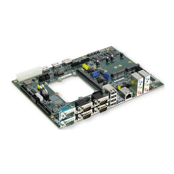
Page 7: Product Overview
LEC-BASE MINI where the carrier board becomes a design platform for testing and developing your applications. Figure 1-1 provides an overview photo of the LEC-BASE MINI with call outs of its interface hardware. The proceeding chapters and sections in this manual present these features in more detail. -
Page 8: Features
Features SMARC interface MXM3 connector PCI Express Bus 3x PCIe x1 links 1x PCIE x1 slot 2x PCIE Mini slots Serial Port UART interfaces (4x UART) Null Modem RS-232 on serial ports COM0 - COM3 ... -
Page 9: Ordering Information
PWM Buttons Boot Select Ordering Information Table 1-1: LEC-BASE MINI Models Model Number Description Second generation SMARC evaluation carrier with triple display (RGB LCD, SC LVDS and HDMI). This version is the standard config- LEC-BASE MINI Standard... -
Page 10: Block Diagram
Block Diagram Figure 1-2 presents a functional representation of the carrier. Figure 1-2: Functional Block Diagram 4 Product Overview... -
Page 11: Specifications
1.5.3 Environmental Most components on the LEC-BASE MINI carrier are selected as extended temperature range parts (-40°C to +85°C). Some components are not available in this temperature range. In these cases, the component temperature ranges are narrower. The LEC-BASE MINI is validated in the -40°C to +85°C range. -
Page 12: Mechanical
Figure 1-3 provides the mechanical dimensions and mounting hole sizes of the LEC-BASE MINI. The LEC-BASE MINI can be mounted to a chassis using M4, B-head screws. Mezzanine cards can be mounted to the carrier using female-female standoffs with M2.5 threads and M2.5, B-head screws. -
Page 13: Hardware
Hardware This chapter describes the physical specifications of the interface connectors, headers, LEDs, and switches on the LEC-BASE MINI. The third section of this chapter further describes the industry standard IO hardware on the carrier. Interface Headers, Jumper Headers, Switches, LEDs, and Connectors Table 2-1 describes the headers, switches, LEDs, and connectors for the LEC-BASE MINI baseboard shown in Figure 2-1, Figure 2-2, and Figure 2-3. - Page 14 Table 2-1: Header, Switch, LED, and Connector Descriptions (Continued) CN22 SPDIF I/O (CODEC) 4-pin, 2mm header for SPDIF digital audio interface from the carrier CODEC [SAMTEC, TMM-102-01-T-D-SM] CN25 LVDS 34-pin, 2mm header for LVDS output [JIHVEI, 23N6850-34S10B-01G-G, BLACK] CN26 LVDS Voltage Select 6-pin, 2mm jumper header for selecting display and backlight LVDS voltages [JIHVEI, 27S1001-OPS35-01G-B, BLACK]...
- Page 15 LEC-BASE MINI Table 2-1: Header, Switch, LED, and Connector Descriptions (Continued) CN52 Fan, Voltage Select 3-pin, 2.54mm jumper header to select FAN supply voltage [NELTRON,2317SJ-06, WHITE] CN53 4-pin, 2.54mm header for CPU fan signals [JVE, 24W1163-04S10-01T-02] CN54 SPI Power, Voltage 3-pin, 2.54mm jumper header for selecting voltages for SPI...
- Page 16 Table 2-1: Header, Switch, LED, and Connector Descriptions (Continued) CN73 PCie2 Mini, Latch Latch for fastening PCI Express Mini card [Attend, 119A-LATCH-80] CN74 PCie2 Mini, Latch Latch for fastening PCI Express Mini card [Attend, 119A-LATCH-80] CN75 PCie2 Mini, Latch Latch for fastening PCI Express Mini card [Attend, 119A-LATCH-80] CN76 PCie2 Mini, Latch...
- Page 17 LEC-BASE MINI Table 2-1: Header, Switch, LED, and Connector Descriptions (Continued) DP Control 8-pole, 1.27mm dip switch for Display Port control [WINWIN, DHN-08-T-V, BLACK] Note: Refer to the PI3EQXDP1201, Display Port Redriver data sheet for more details. CN18 CN14 CN73...
- Page 18 Figure 2-2 illustrates the faces of the standard interface connectors mounted along one edge of the carrier. These connectors are for CAN, Serial Port, USB, Ethernet, and Audio industry-stan- dard cable connectors. CAN1 COM0 COM1 USB5 USB1 (CN78) CAN0 COM2 USBSS0 Audio Audio USB6...
-
Page 19: Standard Hardware References
2.2.1 Audio IO Jacks The LEC-BASE MINI provides two standard audio jacks for HD (CN21) and I2S (CN56) audio. Two audio codecs support these two interfaces. Figure 2-4 depicts the three lines of the audio jacks: Line In (1 - Blue), Line Out (2 - Green), and MIC In (3 - Pink). Figure 2-5 presents the functional block diagram of I2S signals and hardware on the carrier. -
Page 20: Pcie Mini Card Slot
2.2.2 PCIe Mini Card Slot The LEC-BASE MINI provides two standard PCI Express Mini Card slots. Figure 2-6 presents one mini card slot with one of the two fastening latches. Figure 2-7 illustrates the functional block diagram of the PCIe Mini Card signals and hardware on the carrier. -
Page 21: Sdio Slot
LEC-BASE MINI 2.2.3 SDIO Slot The SDIO slot (CN18) provides the standard 4-bit, push-push interface for SD memory cards. LED5 provides indication of SD power. SD cards that operate with only 1.8V, are not sup- ported. Figure 2-8: SDIO Slot... -
Page 22: Sim Slot
2.2.4 SIM Slot Two SIM slots (CN8 / CN10) provide interface for two Subscriber Identity Modules, supporting both PCIe Mini Card slots: CN8 supports CN7 MINI Card slot and CN10 supports CN9 MINI Card slot. Figure 2-9 illustrates the slots’ hinge-type connections. Table 2-3 and Table 2-4 pro- vide the signals for both slots. -
Page 23: Battery Socket
LEC-BASE MINI 2.2.5 Battery Socket One vertical, AAA battery socket provides power for an external RTC coin cell battery. Figure 2-10 illustrates the top and side views of the socket. Table 2-5 provides the signals for socket. Figure 2-10: Battery Socket... - Page 24 Hardware...
-
Page 25: Interfaces
This section provides the pin signals for all the non-standard user interfaces on the LEC-BASE MINI. Unless pinouts for industry standard interfaces have been modified, those pin- out tables will not appear in this manual. Signal definitions for standard interfaces such as SATA, USB, and PCIe can be found in their respective specification datasheets. -
Page 26: Atx Power (Cn2)
ATX Power (CN2) Table 3-1 lists the signals of the standard ATX Power connector, which provides 24 pins, 2 rows consecutive pin sequence (1, 13) with 4.20mm pitch. Use the SW1 button switch on the carrier to apply power to the module. Table 3-1: ATX Power Signals (CN2) Pin# Signal... -
Page 27: Atx Power Supply Enable (Cn4)
LEC-BASE MINI ATX Power Supply Enable (CN4) Table 3-2 lists the pin signals of the ATX Power Supply jumper header, which provides 2 pins with 2.00mm pitch. Table 3-3: ATX Power Supply (CN4) Pin # Signal Jumper Position • Jumper Installed (1-2) - ATX switched rails / power... -
Page 28: Sdmmc Interface (Cn20)
SDMMC Interface (CN20) Table 3-5 lists the pin signals of the SD Card ground plane socket, which provides 60-pins, 2 rows, odd/even pin sequence (1, 2) with 0.50mm pitch. These signals are connected to the SD/ eMMC interface at pins S26 through S36 of the SMARC connector over a 3.3 volt level shifter. Table 3-5: SD/eMMC Interface Signals (CN20) Pin # Signal... -
Page 29: Spdif I/O [Codec] (Cn22)
LEC-BASE MINI Table 3-5: SD/eMMC Interface Signals (CN20) (Continued) Ground Ground Ground Ground MMC_D7 MMC data bit7 Ground Ground Ground Ground Ground MMC_CK MMC clock Ground Ground Ground Ground Ground MMC_CMD MMC command Ground Ground Ground NOTE: The shaded table cells denote power or ground. -
Page 30: Display Interfaces
Table 2-1 of Chapter 2. Figure 3-2 illus- trates the carrier’s two standard and custom display configurations available under separate model order numbers. LEC-BASE MINI Standard LCD R GB LCD R GB... -
Page 31: Lcd Rgb (Cn17)
LEC-BASE MINI 3.8.2 LCD RGB (CN17) Table 3-8 lists the pin signals of the LCD RGB header, which provides 34-pins, 2 rows, odd/even pin sequence (1, 2) with 2.00mm pitch. These pins are connected directly to the LCD interface at the SMARC connector. -
Page 32: Lvds (Cn25)
3.8.3 LVDS (CN25) Table 3-9 lists the pin signals of the LVDS header which provides 34-pins, 2 rows, odd/even pin sequence (1, 2) with 2.00mm pitch. Channel A pins are connected directly to the LVDS interface at the SMARC connector. Channel B pins are connected to selected LCD pins on the SMARC connector Table 3-9: LVDS Interface Pin Signals (CN25) Pin #... -
Page 33: Lvds Voltage Select (Cn26)
LEC-BASE MINI 3.8.4 LVDS Voltage Select (CN26) Table 3-10 lists the pin signals of the LVDS Voltage Select jumper header, which provides 6 pins in two rows with odd/even pin sequence (1,2) and 2.00mm pitch. Table 3-10: LVDS Voltage Select Signals (CN26) -
Page 34: Can0 Termination (Cn29)
Table 3-13: CAN1 Signals (CN28) Pin # Signal Not Connected CAN1_H Not Connected Not Connected GND_CAN Not Connected CAN1_L Not Connected 5 Volt NOTE: These pins are connected over the CAN transceiver to the CAN1 SMARC connector interface (pins P145 and P146.) Shaded table cell denotes power. 3.10 CAN0 Termination (CN29) Table 3-14 lists the pin signals of the CAN0 termination jumper header, which provides 2 pins with 2.00mm pitch. -
Page 35: Spi1 (Cn32)
LEC-BASE MINI Table 3-16: SPI0 Signals (CN31) (Continued) +VCC_SPI SPI0_CN_CLK Not Connected SPI0_CN_MOSI SPI0_CN_MISO NOTE: Shaded table cells denote power or ground. The # symbol indicates the signal is Active Low. 3.13 SPI1 (CN32) Table 3-17 lists the pin signals of the Serial Peripheral Interface 1 header, which provides 10 pins in two rows with odd/even pin sequence (1,2) and 2.54mm pitch. -
Page 36: Com1 And Com3 (Cn34)
Table 3-19: COM2 Signals (CN33) Pin # Signal Not Connected COM2_RX COM2_TX Not Connected Not Connected COM2_RTS# COM2_CTS# Not Connected NOTE: Shaded table cell denotes ground. The # symbol indicates the signal is Active Low. 3.14.2 COM1 and COM3 (CN34) Table 3-20 and Table 3-21 list the pin signals of the Serial B, 2-wire RS232 interface (COM1 and COM3), which provides standard dual DB9 connectors. -
Page 37: Gpio 0-3 (Cn35)
LEC-BASE MINI 3.15 GPIO 0-3 (CN35) Table 3-22 lists the pin signals of the General Purpose IO 0-3 header, which provides 10 pins in 2 rows, odd/even pin sequence (1, 2), and 2.54mm pitch. Table 3-22: General Purpose IO 0-3 (CN35) - Page 38 Table 3-23: Alternate Function Block Interface Pin Signals (CN37) Pin # Signal Alternate Function +V5P0A +V5P0A +V5P0A +V5P0A AFB0_OUT (connected to SMARC pin S17) PMU_SLP_S3# on Intel SOC for S3, Suspend to RAM AFB_DIFF0+ (connected to SMARC pin S62) USB3_TXP on Intel SOC for USB Super-Speed, positive signal of pair AFB1_OUT (connected to SMARC pin S18)
-
Page 39: Gpio 4-7 (Cn39)
LEC-BASE MINI Table 3-23: Alternate Function Block Interface Pin Signals (CN37) (Continued) AFB_DIFF4+ (connected to SMARC pin S74) SATA1_RXP on Intel SOC for SATA high-speed, positive signal of pair AFB8_PTIO (connected to SMARC pin S55) Reserved AFB_DIFF4- (connected to SMARC pin S75) -
Page 40: Gpio 8-11 (Cn41)
3.18 GPIO 8-11 (CN41) Table 3-25 lists the pin signals of the General Purpose IO 8-11 header, which provides 10 pins in 2 rows, odd/even pin sequence (1, 2), and 2.54mm pitch. Table 3-25: General Purpose IO 8-11 (CN41) Pin # Signal +V5P0A CN_GPIO8 (connected to SMARC pin P116) -
Page 41: I2S1 (Cn44)
LEC-BASE MINI 3.20 I2S1 (CN44) Table 3-27 lists the pin signals of the I2S1 header, which provides 8 pins in a single row with 2.54mm pitch. Table 3-27: I2S1 Signals (CN44) Pin # Signal I2S1_LRCK (connected to SMARC pin S43) -
Page 42: Battery Enable (Cn46)
3.22 Battery Enable (CN46) Table 3-29 lists the pin signals of the coin cell battery enable jumper header, which provides 2 pins with 2.00mm pitch. Table 3-29: Battery Enable (CN46) Pin # Signal Jumper Position 3V_BAT • Jumper Installed (1-2) - coin cell battery socket enabled (Default) +VDD_RTC •... -
Page 43: Fan (Cn53)
LEC-BASE MINI 3.25 FAN (CN53) Table 3-32 lists the pin signals of the CPU fan header, which provides 3 pins in a single row with 2.54mm pitch. Table 3-32: FAN (CN53) Pin # Signal FAN_TACH_IN FAN_PWM_OUT NOTE: Shaded table cells denote ground. -
Page 44: I2S0_Sdin Codec Select (Cn58)
3.29 I2S0_SDIN Codec Select (CN58) Table 3-36 lists the pin signals of the I2S0_SDIN Codec Select jumper header, which provides 3 pins in a single row with 2.00mm pitch. Table 3-36: I2S0_SDIN Codec Select (CN58) Pin # Signal Jumper Position I2S0_SDIN_C1 •... -
Page 45: Lin_L Codec Select (Cn62)
LEC-BASE MINI 3.33 LIN_L Codec Select (CN62) Table 3-40 lists the pin signals of the LIN_L Codec Select jumper header, which provides 3 pins in a single row with 2.00mm pitch. Table 3-40: LIN_L Codec Select (CN62) Pin # Signal... -
Page 46: Mic_Bias Codec Select (Cn66)
3.37 MIC_BIAS Codec Select (CN66) Table 3-44 lists the pin signals of the MIC_BIAS Codec Select jumper header, which provides 3 pins in a single row with 2.00mm pitch. Table 3-44: MIC_BIAS Codec Select (CN66) Pin # Signal Jumper Position MIC_BIAS_C1 •... -
Page 47: I2C Gp (Cn70)
LEC-BASE MINI 3.41 I2C GP (CN70) Table 3-48 lists the pin signals of the I2C GP header, which provides 3 pins in a single row with 2.00mm pitch. Table 3-48: I2C GP (CN70) Pin # Signal I2C_GP_CK_3V I2C_GP_DAT_3V Ground NOTE: Shaded table cell denotes ground. -
Page 48: Vin_Pwr_Bad Source Select (Cn81)
Table 3-51: Camera, PCAM / CSI Signals (CN80) (Continued) PCAMD5_CSI1D1N_R Not Connected PCAMD4_CSI1D1P_R Not Connected CAM_MCK_R PCAMD3_CSI1D0N_R PCAMD2_CSI1D0P_R CAM1_1V8 CAM1_1V8 PCAMD1_CSI1CKN_R CAM0_1V8 PCAMD0_CSI1CKP_R CAM0_1V8 CSI0_D1_N_R CAM_VSYS CSI0_D1_P_R CAM_VSYS CAM_VSYS CSI0_D0_N_R CSI0_D0_P_R +V1P5S I2C_CAM_CK_R CSI0_CK_N_R I2C_CAM_DAT_R CSI0_CK_P_R CAM0_PWR#_R CAM1_RST#_R PCAM_FLD_R CAM1_PWR#_R PCAM_DE_R CAM0_RST#_R PCAM_VSYNC_R... -
Page 49: Batman Smbus Voltage Select (Cn82)
LEC-BASE MINI 3.46 BatMan SMBus Voltage Select (CN82) Table 3-53 lists the pin signals of the BatMan SMBus voltage select jumper header, which pro- vides 3 pins in a single row with 2.00mm pitch. Table 3-53: BatMan SMBus Voltage Select (CN82) - Page 50 Interfaces...
-
Page 51: Appendix A Technical Support
LEC-BASE MINI Appendix A Technical Support ADLINK Technology, Inc. provides a number of methods for contacting Technical Support listed in Table A-1 below. Requests for support through Ask an Expert are given the highest priorities, and usually will be addressed within one working day. - Page 52 +49 (0) 991 290 94 – 10 Fax: +49 (0) 991 290 94 - 29 Email: emea@adlinktech.com ADLINK Technology, Inc. (French Liaison Office) Address: 6 allée de Londres, Immeuble Ceylan 91940 Les Ulis, France Tel: +33 (0) 1 60 12 35 66...
- Page 53 84 Genting Lane #07-02A, Cityneon Design Centre Singapore 349584 Tel: +65-6844-2261 Fax: +65-6844-2263 Email: singapore@adlinktech.com ADLINK Technology Singapore Pte. Ltd. (Indian Liaison Office) Address: #50-56, First Floor, Spearhead Towers Margosa Main Road (between 16th/17th Cross) Malleswaram, Bangalore - 560 055, India Tel: +91-80-65605817, +91-80-42246107 Fax:...
Need help?
Do you have a question about the LEC-BASE MINI and is the answer not in the manual?
Questions and answers