Table of Contents
Advertisement
Quick Links
Advertisement
Table of Contents

Related Manuals for ADLINK Technology SMARC MODULE LEC-EL


Summary of Contents for ADLINK Technology SMARC MODULE LEC-EL
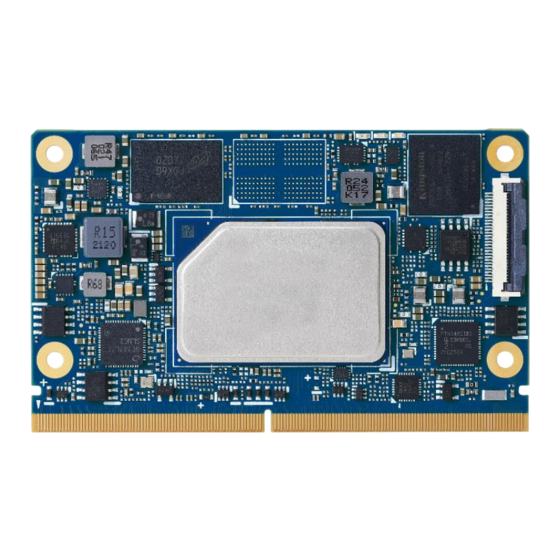
- Page 1 LEC-EL 11/08/2021...
- Page 2 Product names mentioned herein are used for identification purposes only and may be trademarks and/or registered trademarks of their respective companies. © Copyright 2017 ADLINK Technology, Incorporated This document contains proprietary information protected by copyright. All rights are reserved. No part of this manual may be reproduced by any mechanical, electronic, or other means in any form without prior written permission of the manufacturer.
- Page 3 Caution: This information indicates the possibility of minor physical injury, component damage, data loss, and/or program corruption. Warning: This information warns of possible serious physical injury, component damage, data loss, and/or program corruption. Page 3 copyright © 2021 ADLINK Technology Inc.
- Page 4 ADLINK Technology Inc. LEC-EL Product specification Revision History Revision Description Date (dd/mm/yyyy) Author Preliminary engineering version 15/03/2021 Preliminary engineering version updated 25/10/2021 Release version 21/11/2021 Page 4 copyright © 2021 ADLINK Technology Inc.
-
Page 5: Table Of Contents
LAN ports ..................................................................5 4.3.9 SDIO ....................................................................7 4.3.10 SPI & ESPI ..................................................................8 4.3.11 SPI0 ....................................................................8 4.3.12 ESPI ....................................................................9 General Purpose I2C ................................................................10 4.4.1 GPIO....................................................................11 4.4.2 UART ....................................................................12 Page 5 copyright © 2021 ADLINK Technology Inc. - Page 6 SMARC pin to controller mapping ..........................................................18 5. Software Support ............................................................. 29 5.1.1 Yocto ....................................................................29 5.1.2 Ubuntu ................................................................... 29 5.1.3 Windows ..................................................................29 6. Mechanical ..............................................................30 7. Thermal Solutions ............................................................ 31 Page 6 copyright © 2021 ADLINK Technology Inc.
- Page 7 LEC-EL Product specification SGET SMARC Rev 2.1 List of Figures Figure 1 – Module function diagram ..............................................14 Figure 2 – Module top/botom side pin numbering ..........................................1 Page 7 copyright © 2021 ADLINK Technology Inc.
-
Page 8: Introduction
Carrier Boards that implement other features such as audio CODECs, touch controllers, wireless devices, etc. The modular approach allows scalability, fast time to market and upgradability while still maintaining low costs, low power and small physical size. SMARC module and carrier specifications are available online at: https://www.sget.org/standards/smarc.html Page 8 copyright © 2021 ADLINK Technology Inc. -
Page 9: Specifications
HDMI 2.0a supporting resolution up to 4K (4096 x 2160 at 60 Hz) LVDS LVDS single/dual channel 24-bit at max. 1920x 1200 over eDP to LVDS bridge optional MIPI DSI DSI 4 lanes at max. 1080p@60fps display output (build option multiplexed with LVDS signal) Page 9 copyright © 2021 ADLINK Technology Inc. -
Page 10: Audio
Four UART interface SER0,2 (Tx/Rx/CTS/RTS) and SER1, SER3 (Tx/Rx) 7- or 8-bit data words, 1 or 2 stop bits, programmable parity (even, odd, or none) Programmable baud rates up to 4 Mbps. Page 10 copyright © 2021 ADLINK Technology Inc. -
Page 11: System Storage
1x SDIO (4-bit) compatible up to version 3.0. eMMC soldered on module 8, 16, 32, 64, 128 GB (build option) either standard or -40+85C temp range Compatible with eMMC specification 4.51 and higher Page 11 copyright © 2021 ADLINK Technology Inc. -
Page 12: Sema® Board Management Controller
No feedback is provided to allow the carrier to signal Power OK to the modules power state machine. When the state Runtime is reached, the module de- asserts CARRIER_STBY#. The carrier then switches on the remaining rails. Page 12 copyright © 2021 ADLINK Technology Inc. -
Page 13: Mechanical And Environmental
5-90% RH operating, non-condensing 5-95% RH storage (and operating with conformal coating) Shock and Vibration IEC 60068-2-64 and IEC-60068-2-27, MIL-STD-202 F, Method 213B, Table 213-I, Condition A and Method 214A, Table 214-I, Condition D Page 13 copyright © 2021 ADLINK Technology Inc. -
Page 14: Block Diagram
TPM 2.0 SER 2/3 Crypto HSUART ATECC608 eSPI eSPI SER 0/1 BMC/EC BOOT Select IT5121 SPI BIOS FSPI 4x I2C SDIO SDIO HDA/I2S HDA/I2S Power Management Figure 1 – Module function diagram Page 14 copyright © 2021 ADLINK Technology Inc. -
Page 15: Pinout And Signal Descriptions
The below tables are a comprehensible list of all signal pins on the MXM 3 connector in the standard specification SMARC 2.1. P156 S156 Figure 2 – Module top/botom side pin numbering Page 1 copyright © 2021 ADLINK Technology Inc. -
Page 17: Signal Terminology Descriptions
1.8V Power Domain: Active while CARRIER_PWRON is high and CARRIER_SBY# is NOT active (i.e. both signals are high) 3.3Vsb 3.3V Power Domain: Active while CARRIER_PWRON is high (regardless of CARRIER_SBY#) 1.8Vsb 1.8V Power Domain: Active while CARRIER_PWRON is high (regardless of CARRIER_SBY#) Page 1 copyright © 2021 ADLINK Technology Inc. - Page 18 S140 I2C_LCD_DAT I2C_LCD_DAT I2C_LCD_DAT Note : LVDS0/LVDS1 are standard supported through a eDP to LVDS bridge on the module Note : eDP can be used by build option, disabling the LVDS0/LVDS1 ports Page 2 copyright © 2021 ADLINK Technology Inc.
- Page 19 Secondary LVDS Channel Differential Pair O LVDS Runtime 100 ohm differential termination across the differential LVDS1_CK- S109 Clock Lines pair at the endpoint of the signal path, usually on the display assembly. Page 3 copyright © 2021 ADLINK Technology Inc.
- Page 20 AC coupled off Module eDP0_AUX- S135 Management and Device Control LCD0_VDD_EN S133 Primary Panel Power Enable 1.8V Runtime Active high CMOS LCD0_BKLT_EN S127 Primary Panel Backlight Enable 1.8V Runtime Active high CMOS Page 4 copyright © 2021 ADLINK Technology Inc.
- Page 21 HDMI_CK+ DP1_LANE3+ P101 HDMI_CK+ DP1_LANE3+ P102 HDMI_CK- P102 HDMI_CK- DP1_LANE3- DP1_LANE3- S105 HDMI_CTRL_CK DP1_AUX+ S105 HDMI_CTRL_CK DP1_AUX+ S106 HDMI_CTRL_DAT DP1_AUX- S106 HDMI_CTRL_DAT DP1_AUX- P104 HDMI_HPD DP1_HPD P104 HDMI_HPD DP1_HPD P107 DP1_AUX_SEL Note: Page 5 copyright © 2021 ADLINK Technology Inc.
- Page 22 HDMI_HPD P104 HDMI Hot plug active high detection signal 1.8V runtime PD 1M Module must tolerate high level in stand-by mode that serves as an interrupt request CMOS Page 2 copyright © 2021 ADLINK Technology Inc.
- Page 23 HDA_RST# / P112 High Definition Audio reset output 1.8V / 1.5V Runtime GPIO4 to codec, low active. CMOS Note: support for I2S1 signalling pins has been removed during update to SMARC 2.0 specification Page 3 copyright © 2021 ADLINK Technology Inc.
-
Page 24: Usb Ports
USB over-current sense for I/O OD 3.3Vsb / Standby PU 10k Pulled low by Module OD driver to disable USB0 port 2 CMOS 3.3V power. Pulled low by Carrier OD driver to indicate over-current situation. Page 4 copyright © 2021 ADLINK Technology Inc. - Page 25 Standby PU 10k Pulled low by Module OD driver to disable USB0 port 5 CMOS 3.3V power. Pulled low by Carrier OD driver to indicate over-current situation. Note: All USB connected straight from SoC , no support for OTG Page 1 copyright © 2021 ADLINK Technology Inc.
-
Page 26: Pcie Ports
Differential PCIe link C transmit data O LVDS Runtime Series AC coupled on module PCIE_C_TX- pair PCIE PCIE_C_RX+ Differential PCIe link C receive data I LVDS Runtime Series AC coupled off module PCIE_C_RX- pair PCIE Page 2 copyright © 2021 ADLINK Technology Inc. - Page 27 Series AC coupled off module PCIE_D_RX- pair PCIE PCIE_WAKE# S146 PCIe wake up interrupt to host – I OD 3.3V Standby PU 10k common to PCIe links A, B, C, D CMOS Note: Page 3 copyright © 2021 ADLINK Technology Inc.
-
Page 28: Sata Gen 3 Ports
Serial ATA channel 0, Receive Input differential pair. I SATA Runtime Series AC coupled on Module 10 nF SATA0_RX- SATA_ACT# SATA activity indicator O OD 3.3V Runtime Shall be able to sink 24mA or more Carrier LED current CMOS Page 4 copyright © 2021 ADLINK Technology Inc. -
Page 29: Lan Ports
Center-Tap reference voltage for Carrier board Analog 0 to Standby Ethernet magnetic (if required by the Module GBE 3.3V max PHY) GBE0_SDP IEEE 1588 Trigger Signal. For hardware 3.3V Standby implementation of PTP (precision time protocol) CMOS Page 5 copyright © 2021 ADLINK Technology Inc. - Page 30 IEEE 1588 Trigger Signal. For hardware 3.3V Standby implementation of PTP (precision time protocol) CMOS Note: Both LAN interfaces uses a GPY 2.5Gb Ethernet PHY, there is also a 1Gb pin-compatible part Page 6 copyright © 2021 ADLINK Technology Inc.
-
Page 31: Sdio
SDIO_PWR_EN SDIO Power Enable. This signal is used to 3.3V Runtime should be driven low in STB Mode by the module enable the power being supplied to a SD/MMC card CMOS device. Page 7 copyright © 2021 ADLINK Technology Inc. -
Page 32: Spi & Espi
Standby See ESPI CMOS SPI1_DO SPI1 Master output / Slave input 1.8V Standby See ESPI CMOS Note: SPI0 is free to use on the carrier but support only one device through CS0 Page 8 copyright © 2021 ADLINK Technology Inc. -
Page 33: Espi
ESPI_IO_1 can also be used as SPI1_DIN (MISO) ESPI_IO_2 ESPI_IO_3 In Single I/O mode, ESPI_IO_0 is the eSPI master output / eSPI slave input (MOSI) whereas ESPI_IO_1 is the SPI master input / eSPI slave output (MISO). Page 9 copyright © 2021 ADLINK Technology Inc. -
Page 34: General Purpose I2C
I2C clock for serial camera data support link MIPI CSI table I2C_PM_DAT P122 Power management I2C bus DATA (SMBus for x86) Power and System Management I2C_PM_CK P121 Power management I2C bus CLK (SMBus for x86) Power and System Management Page 10 copyright © 2021 ADLINK Technology Inc. -
Page 35: Gpio
PU 470K on the Module CMOS GPIO12 S142 General purpose I/O pin 12 1.8V Runtime PU 470K on the Module CMOS GPIO13 S123 General purpose I/O pin 13 1.8V Runtime PU 470K on the Module CMOS Page 11 copyright © 2021 ADLINK Technology Inc. -
Page 36: Uart
"Clear to Send" handshake line for port 2 1.8V Runtime CMOS SER3_TX P140 Asynchronous serial data output port 3 1.8V Runtime CMOS SER3_RX P141 Asynchronous serial data input port 3 1.8V Runtime CMOS Page 12 copyright © 2021 ADLINK Technology Inc. -
Page 37: Can Bus
Driven by OD on depended on particular module design. Carrier Board Carrier should leave this pin floating for normal operation WDT_TIME_OUT# S145 Watch-Dog-Timer Output, low active. 1.8V Runtime Driven only during runtime CMOS Page 13 copyright © 2021 ADLINK Technology Inc. -
Page 38: Power And System Management
Reset input from Carrier board. Carrier drives low to I OD 1.8V Runtime PU 4.7K Driven by OD on Carrier. force a Module reset, floats the line otherwise. CMOS Pulled up on module. Page 14 copyright © 2021 ADLINK Technology Inc. - Page 39 PU 2k2 On x86 systems these serve as SMB CLK. CMOS Pulled up on module. SMB_ALERT_1V8# SMBus Alert# (interrupt) signal I OD 1.8V Runtime PU 2k2 only used on x86 design CMOS Page 15 copyright © 2021 ADLINK Technology Inc.
-
Page 40: Boot Select
Force Recovery mode – such as over a Serial Port. For x86 systems this signal may be used to load BIOS defaults. Pulled up on Module. Driven by OD part on Carrier. Page 16 copyright © 2021 ADLINK Technology Inc. -
Page 41: Power
S119, S124, S130, S136, S143, S158 VDD_RTC S147 Low current RTC circuit backup [2 to 3.25] / 3.25V power – 3.0V nominal. May be sourced from a Carrier based Lithium cell or Super Cap. Page 17 copyright © 2021 ADLINK Technology Inc. -
Page 42: Smarc Pin To Controller Mapping
ADLINK Technology Inc. LEC-EL Product specification SMARC pin to controller mapping Page 18 copyright © 2021 ADLINK Technology Inc. - Page 43 GPIO / 3.3V LED_0 VDDIO GBE0_MDI1- Bi-Dir GBE MDI TD_M_B VDDIO GBE0_MDI1+ Bi-Dir GBE MDI TD_P_B VDDIO GBE0_CTREF GBE0_MDI0- Bi-Dir GBE MDI TD_M_A VDDIO GBE0_MDI0+ Bi-Dir GBE MDI TD_P_A VDDIO SPI0_CS1# N.C. N.C. Page 19 copyright © 2021 ADLINK Technology Inc.
- Page 44 EL x6000 ECSPI1_MOSI NVCC_ECSPI ALT0 USB0+ Bi-Dir EL x6000 USB1_DP USB1_VDD33 USB0- Bi-Dir EL x6000 USB1_DN USB1_VDD33 USB0_EN_OC# PU-10K GPIO / 3.3V EL x6000 GPIO1_IO13 NVCC_GPIO1 ALT0 USB0_VBUS_DET EL x6000 USB1_VBUS USB1_VDD33 Page 20 copyright © 2021 ADLINK Technology Inc.
- Page 45 HDMI_D2+ / DP1_LANE0+ HDMI EL x6000 HDMI_TX_P_LN_2 HDMI_AVDDIO HDMI_D2- / DP1_LANE0- HDMI EL x6000 HDMI_TX_N_LN_2 HDMI_AVDDIO HDMI_D1+ / DP1_LANE1+ HDMI EL x6000 HDMI_TX_P_LN_1 HDMI_AVDDIO HDMI_D1- / DP1_LANE1- HDMI EL x6000 HDMI_TX_N_LN_1 HDMI_AVDDIO Page 21 copyright © 2021 ADLINK Technology Inc.
- Page 46 GPIO / 1.8V +1V8SMC P124 BOOT_SEL1# PU-4k7 GPIO / 1.8V +1V8SMC P125 BOOT_SEL2# PU-4k7 GPIO / 1.8V +1V8SMC P126 RESET_OUT# GPIO / 1.8V PB15 +1V8SMC P127 RESET_IN# PU-4K7 GPIO / 1.8V PB14 +1V8SMC Page 22 copyright © 2021 ADLINK Technology Inc.
- Page 47 P156 VDD_IN From Carrier board 3 ~ 5.25 V CSI1_TX+ / I2C_CAM1_CK PU-2k2 I2C3 EL x6000 I2C3_SCL NVCC_I2C ALT0 CSI1_TX- / I2C_CAM1_DAT PU-2k2 I2C3 EL x6000 I2C3_SDA NVCC_I2C ALT0 RSVD N.C. N.C. Page 23 copyright © 2021 ADLINK Technology Inc.
- Page 48 N.C. N.C. PCIE_D_TX- / SERDES_1_TX- N.C. N.C. GBE1_LINK_ACT# GPIO / 3.3V LED1 PCIE_D_RX+ / SERDES_1_RX+ N.C. N.C. PCIE_D_RX- / SERDES_1_RX- N.C. N.C. USB4+ Bi-Dir EL x6000 DS4_DP USB4- Bi-Dir EL x6000 DS4_DM Page 24 copyright © 2021 ADLINK Technology Inc.
-
Page 49: Hda_Sync
N.C. USB5- N.C. N.C. USB3_SSTX+ Serial-0.1uF EL x6000 DS1_TXP USB3_SSTX- Serial-0.1uF EL x6000 DS1_TXM USB3_SSRX+ EL x6000 DS1_RXP USB3_SSRX- EL x6000 DS1_RXM USB3+ Bi-Dir EL x6000 DS1_DP USB3- Bi-Dir EL x6000 DS1_DM Page 25 copyright © 2021 ADLINK Technology Inc. - Page 50 PCIE1_VPH PCIE_B_TX- Serial-0.1uF PCIe EL x6000 PCIE1_TXN_N PCIE1_VPH DP0_LANE0+ N.C. N.C. DP0_LANE0- N.C. N.C. DP0_AUX_SEL N.C. N.C. DP0_LANE1+ N.C. N.C. DP0_LANE1- N.C. N.C. DP0_HPD N.C. N.C. DP0_LANE2+ N.C. N.C. S100 DP0_LANE2- S101 Page 26 copyright © 2021 ADLINK Technology Inc.
- Page 51 Serial-0R LVDS PTN3460 A_Y0N S127 LCD0_BKLT_EN GPIO / 1.8V EL x6000 GPIO1_IO00 S128 LVDS0_1+ / eDP0_TX1+ / Serial-0R LVDS PTN3460 A_Y1P DSI0_D1+ S129 LVDS0_1- / eDP0_TX1- / DSI0_D1- Serial-0R LVDS PTN3460 A_Y1N Page 27 copyright © 2021 ADLINK Technology Inc.
- Page 52 GPIO / 1.8V +1V8SMC S151 CHARGING# PU-68K GPIO / 1.8V EL x6000 SAI5_RXC NVCC_SAI5 ALT5 S152 CHARGER_PRSNT# PU-100K GPIO / 1.8V EL x6000 SAI5_RXD0 NVCC_SAI5 ALT5 S153 CARRIER_STBY# GPIO / 1.8V +1V8SMC Page 28 copyright © 2021 ADLINK Technology Inc.
-
Page 53: Software Support
SGET SMARC Rev 2.1 5. Software Support 5.1.1 Yocto Yocto is available from Adlink Github > https://github.com/ADLINK/meta-adlink-x86-64bit 5.1.2 Ubuntu Ubuntu is supported from kernel 5.15 and up 5.1.3 Windows Windows 10 is supported Page 29 copyright © 2021 ADLINK Technology Inc. -
Page 54: Mechanical
ADLINK Technology Inc. LEC-EL Product specification 6. Mechanical PCB dimension: 82 x 50 x 1.2 mm, 12 layer PCB Page 30 copyright © 2021 ADLINK Technology Inc. -
Page 55: Thermal Solutions
SGET SMARC Rev 2.1 7. Thermal Solutions For optimum performance LEC-EL has to be cooled by a passive Heatsink / Heat-spreader optionally available for ordering HTS-sEL Heatspreader for LEC-EL THS-sEL Low profile heatsink for LEC-EL Page 31 copyright © 2021 ADLINK Technology Inc.
Need help?
Do you have a question about the SMARC MODULE LEC-EL and is the answer not in the manual?
Questions and answers