
Subscribe to Our Youtube Channel
Related Manuals for ADLINK Technology COM-HPC-sIDH


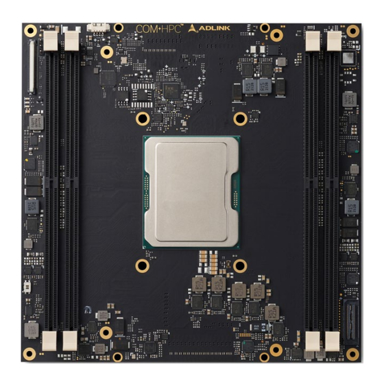
Summary of Contents for ADLINK Technology COM-HPC-sIDH
- Page 1 COM-HPC-sIDH User’s Guide PICMG COM-HPC R1.1 COM-HPC-sIDH User’s Guide Revision: Rev. 0.1 Date: 2023-05-05 Part Number: 50M-00133-1000 Page 1 Copyright © 2023 ADLINK Technology, Inc.
-
Page 2: Revision History
COM-HPC-sIDH User’s Guide PICMG COM-HPC R1.1 Revision History Revision Description Date Author Preliminary release 2023-05-05 Page 2 Copyright © 2023 ADLINK Technology, Inc. -
Page 3: Preface
Product names mentioned herein are used for identification purposes only and may be trademarks / registered trademarks of respective companies. Copyright © 2023 ADLINK Technology Incorporated This document contains proprietary information protected by copyright. All rights are reserved. No part of this manual may be reproduced by any mechanical, electronic, or other means in any form without prior written permission of the manufacturer. - Page 4 Only install/attach and operate equipment on stable surfaces and/or recommended mountings; • If the equipment will not be used for long periods of time, turn off the power source and unplug the equipment. • Page 4 Copyright © 2023 ADLINK Technology, Inc.
- Page 5 Caution: This information indicates the possibility of minor physical injury, component damage, data loss, and/or program corruption. Warning: This information warns of possible serious physical injury, component damage, data loss, and/or program corruption. Page 5 Copyright © 2023 ADLINK Technology, Inc.
- Page 6 ADLINK Technology GmbH Hans-Thoma-Strasse 11, D-68163 Mannheim, Germany Tel: +49-621-43214-0 Fax: +49-621 43214-30 Email: emea@adlinktech.com Please visit the Contact page at www.adlinktech.com for information on how to contact the ADLINK regional office nearest you. Page 6 Copyright © 2023 ADLINK Technology, Inc.
-
Page 7: Table Of Contents
Asynchronous Serial Port ..........................................................43 4.3.7 I2C ..................................................................43 4.3.8 eSPI ..................................................................44 4.3.9 Boot SPI (BIOS ONLY) and Boot Select ....................................................44 4.3.10 Port 80 Support on USB_PD I2C Bus ......................................................45 Page 7 Copyright © 2023 ADLINK Technology, Inc. - Page 8 9.1. Windows Server 2019 64-bit ........................................................... 75 9.2. Windows 10 IoT Enterprise 64-bit ......................................................... 75 9.3. Yocto Linux 64-bit (TBC) ............................................................75 10. Mechanical ..............................................................76 11. Thermal ................................................................ 77 11.1. Thermal Solutions ................................................................ 77 Page 8 Copyright © 2023 ADLINK Technology, Inc.
- Page 9 COM-HPC-sIDH User’s Guide PICMG COM-HPC R1.1 11.1.1 Heatspreader: HTS ............................................................77 11.1.2 Heatsink: THS-BL .............................................................. 78 11.1.3 Heatsink with Fan: THSF ..........................................................79 11.1.4 Heatsink with Fan: THSF-BL-S ........................................................80 Page 9 Copyright © 2023 ADLINK Technology, Inc.
-
Page 10: List Of Figures
Figure 6 – Heatspreader: HTS ........................................................77 Figure 7 – Heatsink: THS-BL ........................................................78 Figure 8 – Heatsink with Fan: THSF ......................................................79 Figure 9 – Heatsink with Fan: THSF-BL-S ....................................................80 Page 10 Copyright © 2023 ADLINK Technology, Inc. -
Page 11: Introduction
AI. The COM-HPC-sIDH has up to four DIMM sockets supporting up to 256GB (4x 64GB) of DDR4 RDIMM memory, or even higher with LRDIMM. It provides a memory frequency of up to 3200 MT/s, dependent on system configuration. -
Page 12: Specifications
Up to 2933 MT/s for D-2796TE/D-2775TE, 2667 MT/s for D-2752TER/D-2733NT/D-2712T 1 DIMM per channel architecture for maximum performance Embedded BIOS AMI Aptio V UEFI with CMOS backup in 64 (or 32, TBC) MB SPI BIOS, dual BIOS by build option Page 12 Copyright © 2023 ADLINK Technology, Inc. -
Page 13: Expansion Busses
Note: PCIe 8-11 should be used for the first NVMe instance and PCIe 12-15 should be used for the second NMVe instance. These are recommended by COM-HPC specifications. Other: SMBus (system), 2x I2C (user, I2C_0, I2C_1, I2C_0 offers ALERT#), eSPI bus Page 13 Copyright © 2023 ADLINK Technology, Inc. -
Page 14: Ethernet Kr
10G BASE-T (1pc, X557-AT4 on carrier) Note: 1. Firmware for each configuration may differ and is dependent on silicon vendor. 2. Table above shows highest speed supported per lane and can be configured to lower speeds. Page 14 Copyright © 2023 ADLINK Technology, Inc. -
Page 15: Ethernet Nbase-T
2x SATA 6Gb/s (SATA 0, 1) Note: HSIO combined bandwidth support can be up to the equivalence of 16 PCIe Gen3 lanes. PCIe lane 0-15, SATA, USB High-speed SSTX/RX pair, NBASE-T, and PCIe_BMC are sourced from HSIO. Page 15 Copyright © 2023 ADLINK Technology, Inc. - Page 16 Carrier BMC_UART_0. The Carrier BMC_UART_0 IRQ is 9, Address is 0x220. 3. Carrier BMC_UART_1 and Module_UART_1 connect to a pin header of COM-HPC Server Base. It can be used as console module. The Carrier BMC_UART_1 IRQ is 10, Address is 0x228. Page 16 Copyright © 2023 ADLINK Technology, Inc.
-
Page 17: Trusted Platform Module (Tpm)
MMC, Module Management Controller It works in conjunction with Carrier BMC through IPMB and/or UART, I2C Reacts with Carrier BMC, e.g. forwarding COM-HPC module’s temperature, voltage, FAN speed, board information to Carrier BMC. Page 17 Copyright © 2023 ADLINK Technology, Inc. -
Page 18: Debug
PICMG COM-HPC Rev 1.1, Server Type, Size D 160 x 160 mm Operating Temperature Standard 0°C to 60°C (Standard Voltage Input) Storage: -20°C to 80°C Extreme Rugged -40°C to 85°C (Standard Voltage Input) Storage: -40°C to 85°C (Selected SoC SKUs) Page 18 Copyright © 2023 ADLINK Technology, Inc. - Page 19 Shock and Vibration IEC 60068-2-64 and IEC-60068-2-27 MIL-STD-202F, Method 213B, Table 213-I, Condition A and Method 214A, Table 214-I, Condition D HALT tested Thermal Stress, Vibration Stress, Thermal Shock and Combined Test Page 19 Copyright © 2023 ADLINK Technology, Inc.
-
Page 20: Block Diagram
EEPROM (FRU) I2C 0 (w/ ALERT#) I2C 1 UART 0-1 iMC 0 iMC 1 HSUART eSPI SEMA 12x GPIO Board Controller DIMM DIMM DIMM DIMM IPMB eSPI Figure 1 – Module function diagram Page 20 Copyright © 2023 ADLINK Technology, Inc. -
Page 21: Pinout And Signal Descriptions
The table below is a comprehensive list of all signal pins supported on the dual 400-pin COM-HPC connectors as defined for Server Type in the PICMG COM-HPC R1.1 specification. Signals described in the specification but not supported on the COM-HPC-sIDH are marked by STRIKETHROUGH. - Page 22 ETH2_TX- ETH2_RX+ ETH6_RX+ USB23_OC# ETH2_TX+ USB01_OC# ETH3_RX- ETH7_RX- SML1_CLK ETH3_TX- ETH3_RX+ ETH7_RX+ SML1_DAT ETH3_TX+ PMCALERT# USB3_SSTX- RSVD SML0_CLK USB3_SSRX- USB3_SSTX+ RSVD SML0_DAT USB3_SSRX+ USB_PD_ALERT# USB2_SSTX- ETH4_TX- USB_PD_I2C_CLK USB2_SSRX- USB2_SSTX+ ETH4_TX+ USB_PD_I2C_DAT USB2_SSRX+ Page 22 Copyright © 2023 ADLINK Technology, Inc.
- Page 23 PCIe08_RX- PCIe00_TX- PCIe08_TX- PCIe08_RX+ PCIe00_RX- PCIe00_TX+ PCIe08_TX+ PCIe00_RX+ PCIe09_RX- PCIe01_TX- PCIe09_TX- PCIe09_RX+ PCIe01_RX- PCIe01_TX+ PCIe09_TX+ PCIe01_RX+ PCIe10_RX- PCIe02_TX- PCIe10_TX- PCIe10_RX+ PCIe02_RX- PCIe02_TX+ PCIe10_TX+ PCIe02_RX+ PCIe11_RX- PCIe03_TX- PCIe11_TX- PCIe11_RX+ PCIe03_RX- PCIe03_TX+ PCIe11_TX+ PCIe03_RX+ Page 23 Copyright © 2023 ADLINK Technology, Inc.
- Page 24 GPIO_06 GPSPI_MISO I2C0_DAT NBASET0_MDI3- GPIO_07 GPSPI_CS0# I2C0_ALERT# NBASET0_MDI3+ GPIO_08 GPSPI_CS1# I2C1_CLK GPIO_09 GPSPI_CS2# I2C1_DAT NBASET0_LINK_MAX# GPIO_10 GPSPI_CS3# NBASET0_SDP * NBASET0_LINK_MID# GPIO_11 GPSPI_CLK NBASET0_CTREF NBASET0_LINK_ACT# A100 TYPE0 B100 GPSPI_ALERT# C100 TYPE1 D100 TYPE2 Page 24 Copyright © 2023 ADLINK Technology, Inc.
- Page 25 PCIe33_TX+ PCIe41_RX+ PCIe34_RX- PCIe42_TX- PCIe34_TX- PCIe34_RX+ PCIe42_RX- PCIe42_TX+ PCIe34_TX+ PCIe42_RX+ PCIe35_RX- PCIe43_TX- PCIe35_TX- PCIe35_RX+ PCIe43_RX- PCIe43_TX+ PCIe35_TX+ PCIe43_RX+ PCIe36_RX- PCIe44_TX- PCIe36_TX- PCIe36_RX+ PCIe44_RX- PCIe44_TX+ PCIe36_TX+ PCIe44_RX+ PCIe37_RX- PCIe45_TX- PCIe37_TX- PCIe37_RX+ PCIe45_RX- PCIe45_TX+ Page 25 Copyright © 2023 ADLINK Technology, Inc.
- Page 26 PCIe21_TX+ PCIe29_RX+ PCIe22_RX- PCIe30_TX- PCIe22_TX- PCIe22_RX+ PCIe30_RX- PCIe30_TX+ PCIe22_TX+ PCIe30_RX+ PCIe23_RX- PCIe31_TX- PCIe23_TX- PCIe23_RX+ PCIe31_RX- PCIe31_TX+ PCIe23_TX+ PCIe31_RX+ PCIe48_RX- PCIe56_TX- PCIe48_TX- PCIe48_RX+ PCIe56_RX- PCIe56_TX+ PCIe48_TX+ PCIe56_RX+ PCIe49_RX- PCIe57_TX- PCIe49_TX- PCIe49_RX+ PCIe57_RX- PCIe57_TX+ Page 26 Copyright © 2023 ADLINK Technology, Inc.
- Page 27 PCIe_CLKREQ3# PCIe_REFCLKIN1- PCIe_CLKREQ1# ETH0-3_PRSNT# ETH0-3_I2C_CLK PCIe_REFCLKIN1+ PCIe_CLKREQ2# ETH0-3_PHY_RST# ETH0-3_I2C_DAT PCIe_CLKREQ_OUT0# ETH0_SDP ETH0-3_PHY_INT# ETH0-3_MDIO_CLK PCIe_CLKREQ_OUT1# ETH1_SDP ETH0-3_INT# ETH0-3_MDIO_DAT E100 PCIe_PERST_IN0# F100 PCIe_PERST_IN1# G100 PCIe_WAKE_OUT0# H100 PCIe_WAKE_OUT1# Note: NBASET0_SDP depends on LAN controller SK. Page 27 Copyright © 2023 ADLINK Technology, Inc.
-
Page 28: Signal Terminology Descriptions
Pull-down strap. A Module output pin that is either tied to GND or is not connected. Used to signal Module capabilities to the Carrier Board. PU (pull-up) resistor on module PD (pull-down) resistor on module Page 28 Copyright © 2023 ADLINK Technology, Inc. -
Page 29: Signal Descriptions On J1/J2 Connectors
Active low interrupt signal from IO Port expanders for PU 10K ETH ports 0 to 3 3.3VSB 3.3VSB ETH0-3_PHY_INT# Active low PHY interrupt signal from ETH ports 0 to 3 PU 1K Not supported 3.3VSB 3.3VSB Page 29 Copyright © 2023 ADLINK Technology, Inc. - Page 30 ETH6_RX+ ETH7_RX- ETH7_RX+ ETH4-7_MDIO_DAT Management Data I/O interface mode data signal for PU 1K serial data transfers between the MAC and an 3.3VSB 3.3VSB external PHY for ETHx ports 4 to 7 Page 30 Copyright © 2023 ADLINK Technology, Inc.
-
Page 31: Nbase-T Ethernet
Twisted pair signals for external transformer. NBASET0_MDI0+ 0,1,2,3. The MDI can operate in 10Gbps, 1Gbps, 100Mbps and 10 NBASET0_MDI1- Mbps modes. Some pairs are unused in some modes, per the NBASET0_MDI1+ following: NBASET0_MDI2- NBASET0_MDI2+ Page 31 Copyright © 2023 ADLINK Technology, Inc. - Page 32 250 mA or less. NBASET0_SDP NBASE-T Ethernet Controller 0 Software-Definable Pin. Can also be IO 3.3VSB Depends on LAN controller SKU used for IEEE1588 support such as a 1pps signal. Page 32 Copyright © 2023 ADLINK Technology, Inc.
-
Page 33: Pci Express
PCI Express Differential Transmit Pairs 8-15 O PCIe AC coupled on Module PCIe08_TX- PCIe Group 0 High PCIe09_TX+ A Server Module may map up to 8 higher bandwidth PCIe09_TX- PCIe lanes to Group 0 High Page 33 Copyright © 2023 ADLINK Technology, Inc. - Page 34 PCIe13_RX+ PCIe13_RX- PCIe14_RX+ PCIe14_RX- PCIe15_RX+ PCIe15_RX- PCIe16_TX+ PCI Express Differential Transmit Pairs 16-31 O PCIe AC coupled on Module PCIe16_TX- PCIe Group 1 PCIe17_TX+ PCIe17_TX- PCIe18_TX+ PCIe18_TX- PCIe19_TX+ PCIe19_TX- PCIe20_TX+ PCIe20_TX- PCIe21_TX+ Page 34 Copyright © 2023 ADLINK Technology, Inc.
- Page 35 PCI Express Differential Receive Pairs 16-31 I PCIe AC coupled off Module PCIe16_RX- PCIe Group 1 PCIe17_RX+ PCIe17_RX- PCIe18_RX+ PCIe18_RX- PCIe19_RX+ PCIe19_RX- PCIe20_RX+ PCIe20_RX- PCIe21_RX+ PCIe21_RX- PCIe22_RX+ PCIe22_RX- PCIe23_RX+ PCIe23_RX- PCIe24_RX+ PCIe24_RX- Page 35 Copyright © 2023 ADLINK Technology, Inc.
- Page 36 O PCIe AC coupled on Module PCIe32_TX- PCIe Group 2 PCIe33_TX+ PCIe33_TX- PCIe34_TX+ PCIe34_TX- PCIe35_TX+ PCIe35_TX- PCIe36_TX+ PCIe36_TX- PCIe37_TX+ PCIe37_TX- PCIe38_TX+ PCIe38_TX- PCIe39_TX+ PCIe39_TX- PCIe40_TX+ PCIe40_TX- PCIe41_TX+ PCIe41_TX- PCIe42_TX+ PCIe42_TX- PCIe43_TX+ PCIe43_TX- PCIe44_TX+ Page 36 Copyright © 2023 ADLINK Technology, Inc.
- Page 37 PCIe Group 2 PCIe33_RX+ PCIe33_RX- PCIe34_RX+ PCIe34_RX- PCIe35_RX+ PCIe35_RX- PCIe36_RX+ PCIe36_RX- PCIe37_RX+ PCIe37_RX- PCIe38_RX+ PCIe38_RX- PCIe39_RX+ PCIe39_RX- PCIe40_RX+ PCIe40_RX- PCIe41_RX+ PCIe41_RX- PCIe42_RX+ PCIe42_RX- PCIe43_RX+ PCIe43_RX- PCIe44_RX+ PCIe44_RX- PCIe45_RX+ PCIe45_RX- PCIe46_RX+ PCIe46_RX- PCIe47_RX+ PCIe47_RX- Page 37 Copyright © 2023 ADLINK Technology, Inc.
- Page 38 PCIe58_TX+ PCIe58_TX- PCIe59_TX+ PCIe59_TX- PCIe60_TX+ PCIe60_TX- PCIe61_TX+ PCIe61_TX- PCIe62_TX+ PCIe62_TX- PCIe63_TX+ PCIe63_TX- PCIe48_RX+ PCI Express Differential Receive Pairs 48-63 I PCIe Not supported PCIe48_RX- PCIe Group 3 PCIe49_RX+ PCIe49_RX- PCIe50_RX+ PCIe50_RX- PCIe51_RX+ Page 38 Copyright © 2023 ADLINK Technology, Inc.
- Page 39 Reference clock pair for PCIe lanes [16:31], also O PCIe PCIe_REFCLK1+ referred to PCIe Group 1 PCIe_REFCLK2- Reference clock pair for PCIe lanes [32:47], also O PCIe PCIe_REFCLK2+ referred to PCIe Group 2 Page 39 Copyright © 2023 ADLINK Technology, Inc.
-
Page 40: Usb
USB0 may be configured as a USB client or as a host, USB5- or both at the Module designer's discretion. All other USB6+ USB ports, if implemented, shall be host ports. USB6- Page 40 Copyright © 2023 ADLINK Technology, Inc. - Page 41 I PCIe AC coupled off Module USB2_SSRX- USB 3.2 Gen 1 or Gen 2 implementations. USB3_SSRX+ USB3_SSRX- These ports shall be used in conjunction with the corresponding USB 2.0 port pair (e.g. USB2_SSxxx+/- Page 41 Copyright © 2023 ADLINK Technology, Inc.
-
Page 42: Sata
AC coupled on Module SATA0_RX- SATA1_TX+ Serial ATA Channel 1 transmit differential pair. O SATA AC coupled on Module SATA1_TX- SATA1_RX+ Serial ATA Channel 1 receive differential pair. I SATA AC coupled on Module SATA1_RX- Page 42 Copyright © 2023 ADLINK Technology, Inc. -
Page 43: Asynchronous Serial Port
I2C1_CLK Clock I/O line for the general purpose I2C1 port I/O OD PU 4.7K 1.8VSB 1.8VSB I2C1_DAT Data I/O line for the general purpose I2C1 port I/O OD PU 4.7K 1.8VSB 1.8VSB Page 43 Copyright © 2023 ADLINK Technology, Inc. -
Page 44: Espi
(SQI) mode. If the flash memory device is operating BOOT_SPI_IO3 in traditional Serial Peripheral Interface (SPI) mode, then signal BOOT_SPI_IO0 is used for getting serial data into the flash device (referred to as SI or MOSI Page 44 Copyright © 2023 ADLINK Technology, Inc. -
Page 45: Port 80 Support On Usb_Pd I2C Bus
Controller master and Carrier based USB Power 3.3VSB 3.3VSB Delivery Controller slave. USB_PD_ALERT# I2C clock line between Module based Embedded Not Supported Controller master and Carrier based USB Power 3.3VSB Delivery Controller slave. Page 45 Copyright © 2023 ADLINK Technology, Inc. -
Page 46: Ipmb
Not supported GP_SPI_CS0# GP_SPI chip selects, active low O 3.3V Not supported GP_SPI_CS1# GP_SPI_CS2# GP_SPI_CS3# GP_SPI_ALERT# B100 Alert (interrupt) from a Carrier GP_SPI device to the I 3.3V PU 10K Not supported Module Page 46 Copyright © 2023 ADLINK Technology, Inc. -
Page 47: Power & System Management
PU 10K on PS2 keyboard or mouse activity. 3.3VSB BATLOW# Indicates that external battery is low. I 3.3VSB PU 10K This port provides a battery-low signal to the Module for orderly 3.3VSB Page 47 Copyright © 2023 ADLINK Technology, Inc. -
Page 48: Rapid Shutdown
Comment CARRIER_HOT# Input from off-Module temp sensor indicating an I 3.3V PU 100K over-temp situation. 3.3V THERMTRIP# Active low output indicating that the CPU has entered O 3.3V thermal shutdown. 4.99K 3.3V Page 48 Copyright © 2023 ADLINK Technology, Inc. -
Page 49: Smbus
3.3V GPIO_02 inputs. GPIO_03 GPIO_04 As inputs, these pins should be able to generate an GPIO_05 interrupt to the Module host. GPIO_06 GPIO_07 GPIO_08 GPIO_09 GPIO_10 GPIO_11 Page 49 Copyright © 2023 ADLINK Technology, Inc. -
Page 50: Module Type Definition
VCC to the COM-HPC Module) if an incompatible Module pin-out type is detected. All three TYPE[x] pins should be monitored by the Carrier. The Carrier Board logic may also implement a fault indicator such as an LED. Page 50 Copyright © 2023 ADLINK Technology, Inc. -
Page 51: Miscellaneous Signals
3.3V 3.3V RSVD Reserved pins. These may be assigned functions in future versions of this specification. Reserved pins shall not be connected to anything, and shall not be connected to each other. Page 51 Copyright © 2023 ADLINK Technology, Inc. -
Page 52: Power And Ground
Real-time clock circuit-power input. Nominally +3.0V. Ground - DC power and signal and AC signal return path. All available GND connector pins shall be used and tied to Carrier Board GND plane(s). Page 52 Copyright © 2023 ADLINK Technology, Inc. -
Page 53: Additional Features
This chapter describes the connectors, LEDs, and switches, located on the module and are not necessarily included in the PICMG standard specification. The locations of these parts are as shown below: XDP debug header (Chris) Fan Connector 40-pin Debug Connect BIOS Default Reset Figure 3 – Module feature locations (front) Page 53 Copyright © 2023 ADLINK Technology, Inc. -
Page 54: Figure 4 - Module Feature Locations (Bottom)
COM-HPC-sIDH User’s Guide PICMG COM-HPC R1.1 BIOS setting switch MMC switch (for debug only) Figure 4 – Module feature locations (bottom) Page 54 Copyright © 2023 ADLINK Technology, Inc. -
Page 55: Debug Connector (40-Pin Connector)
This connector is particular useful during carrier design and bring up phase. It offers access to the following critical parts of the module: Test points for measurement of internal power rails SPI BIOS programming interface I2C bus for BIOS POST code readout Module EC and MMC programming interface Page 55 Copyright © 2023 ADLINK Technology, Inc. -
Page 56: Status Leds
Rebooted after PWRBTN WD LED = LED OFF Rebooted after RESET BTN WD LED = LED OFF Note: only a Reset not initiated by the BMC can clear the WD LED (user action) Page 56 Copyright © 2023 ADLINK Technology, Inc. -
Page 57: Exception Codes
COM-HPC-sIDH User’s Guide PICMG COM-HPC R1.1 5.3 Exception Codes Exception Code Error Message NOERROR NO_SLP_S5 NO_SLP_S4 NO_SLP_S3 BIOS_FAIL RESET_FAIL NO_CB_PWROK CRITICAL_TEMP POWER_FAIL VOLTAGE_FAIL RSMRST_FAIL NO_VDDQ_PG NO_VCORE_PG NO_SYS_GD NO_V3P3A NO_PWRSRC_GD NO_PCH_PG Page 57 Copyright © 2023 ADLINK Technology, Inc. -
Page 58: Fan Connector
PICMG COM-HPC R1.1 5.4 Fan Connector Connector Type: JVE 24W1125A-04M00 Name Description FAN_PWMOUT FAN_TACHIN 12V* The supply voltage and maximum current of the fan connector is dependent on the module’s input voltage (VCC_12V pins) Page 58 Copyright © 2023 ADLINK Technology, Inc. -
Page 59: Bios Default Reset
Hold down the BIOS Setup Defaults Reset Button continuously and boot up the system. You can release the button when the BIOS prompt screen appears. The BIOS prompt screen will display a confirmation that BIOS defaults have been reset and request that you reboot the system. Page 59 Copyright © 2023 ADLINK Technology, Inc. -
Page 60: Bios Boot Select
In either mode, BIOS Select and Mode Configuration Switch, Pin 1 is used to select whether to boot from SPI0 or SPI1. Mode Pin 1 Pin 2 Boot from SPI0 (default) Boot from SPI1 Set BIOS to PICMG mode (default, TBC) Set BIOS to Failsafe BIOS mode Page 60 Copyright © 2023 ADLINK Technology, Inc. -
Page 61: Mipi 60 Debug Header
TRC_DATA[0][4] TRC_DATA1[4] / TRC_DATA0[24] TRC_DATA[0][5] TRC_DATA1[5] / TRC_DATA0[25] TRC_DATA[0][6] TRC_DATA1[6] / TRC_DATA0[26] TRC_DATA[0][7] TRC_DATA1[7] / TRC_DATA0[27] TRC_DATA[0][8] TRC_DATA1[8] / TRC_DATA0[28] TRC_DATA[0][9] TRC_DATA1[9] / TRC_DATA0[29] TRC_DATA3[0] / TRC_DATA0[10] TRC_DATA2[0] / TRC_DATA1[10] / TRC_DATA0[30] Page 61 Copyright © 2023 ADLINK Technology, Inc. - Page 62 / TRC_DATA0[36] TRC_DATA2[7] / TRC_DATA1[17] TRC_DATA3[7] / TRC_DATA0[17] / TRC_DATA0[37] TRC_DATA2[8] / TRC_DATA1[18] TRC_DATA3[8] / TRC_DATA0[18] / TRC_DATA0[38] TRC_DATA2[9] / TRC_DATA1[19] TRC_DATA3[9] / TRC_DATA0[19] / TRC_DATA0[39] Connect to GND plane TRC_CLK[3] TRC_CLK[2] Page 62 Copyright © 2023 ADLINK Technology, Inc.
-
Page 63: System Resources
FED00000-FED003FF Hight precision event timer FEC00000-FECFFFFF Advance programmable interrupt controller FE200000-FE7FFFFF Motherboard resources FE000000-FE01FFFF Motherboard resources FD6F0000-FDFFFFFF Motherboard resources FD000000-FD69FFFF Motherboard resources E1000000-FB7FFFFF PCI Express Root Complex C6000000-E0FFFFFF PCI Express Root Complex Page 63 Copyright © 2023 ADLINK Technology, Inc. -
Page 64: I/O Map
Serial port 2 (COM4) 3B0h – 3BBh CDF PCIeRP[9]-18AE 3C0h – 3CFh CDF PCIeRP[9]-18AE 3F8h - 3FFh Serial port 1 (COM1) 400h - 41Fh Motherboard resources 4D0h – 4D1h Programmable interrupt controller Page 64 Copyright © 2023 ADLINK Technology, Inc. -
Page 65: Interrupt Request (Irq) Lines
6.3 Interrupt Request (IRQ) Lines IRQ# Typical Intterupt Resource Connected to Pin Available High precision even timer/System timer Serial Port 4 Serial Port 1 System CMOS/Real time clock CDF ME:HECI Numeric data processor Page 65 Copyright © 2023 ADLINK Technology, Inc. -
Page 66: Pci Configuration Space Map
Reserved Internal CPU Intel® Trace Hub Internal Virtual Root Port (VRP) for Intel QAT v1.7 Intel QAT v1.7 (Bus subordinate to S0 VRP is PF: 0 Internal assigned by BIOS) VF: 0-15 Page 66 Copyright © 2023 ADLINK Technology, Inc. - Page 67 Internal SPI Controller Internal PCH Intel® Trace Hub Internal Intel Ethernet controller Internal PCI Bridge External AST2500 Internal Mesh2IIO MMAP/VT-D Internal Mesh2IIO PMON Internal Mesh2IIO RAS Internal Mesh2IIO DFX Internal Mesh2IIO MMAP/VT-D Page 67 Copyright © 2023 ADLINK Technology, Inc.
- Page 68 Intel Ethernet Controller Internal Intel Ethernet Controller Internal Mesh2IIO MMAP/VT-D Internal Mesh2IIO PMON Internal Mesh2IIO RAS Internal Mesh2IIO DFX Internal Satellite IEH Internal UBOX - Global Events Internal UBOX Internal UBOX -DEC Page 68 Copyright © 2023 ADLINK Technology, Inc.
- Page 69 CHA1_GRP0 - UNICAST_GROUP0_CHA Internal CHA2_GRP0 - UNICAST_GROUP0_CHA Internal CHA3_GRP0 - UNICAST_GROUP0_CHA Internal CHA4_GRP0 - UNICAST_GROUP0_CHA Internal CHA5_GRP0 - UNICAST_GROUP0_CHA Internal CHAALL0 - Multicast DRAM Rules Internal CHAALL1 - Multicast MMIO Rules Internal Internal Page 69 Copyright © 2023 ADLINK Technology, Inc.
-
Page 70: Pci Interrupt Routing Map
SMBus con- Controller Port 0 Engine0 Bridge troller on Int0 INTA:16 INTA:16 INTA:16 INTA:16 Int1 INTB:17 INTB:17 Int2 INTC:18 INTC:18 Int3 INTC:19 XHCI Intel I210 Line Controller Int0 INTA:16 INTA:16 Int1 Int2 Int3 Page 70 Copyright © 2023 ADLINK Technology, Inc. -
Page 71: Smbus Address Table
Port 4 Port 5 Port 8 Int0 Int1 Int2 Int3 6.6 SMBus Address Table Device Address DDR4 Channel A(SO-DIMM1) DDR4 Channel B(SO-DIMM2) DDR4 Channel C(SO-DIMM3) DDR4 Channel D(SO-DIMM4) Thermal Sensor Thermal Sensor Page 71 Copyright © 2023 ADLINK Technology, Inc. -
Page 72: Bios Setup
Advanced Power Manage- Bmc self test log► Reserve Memory► ment Configuration► Miscellaneous ► BMC network configuration► Network Stack Config- View System Event Log► uration ► Trusted Computing ► BMC User Settings► BMC warm reset Page 72 Copyright © 2023 ADLINK Technology, Inc. - Page 73 COM-HPC-sIDH User’s Guide PICMG COM-HPC R1.1 Boot Save & Exit Boot Config- Save Options uration Default Options Boot Override Page 73 Copyright © 2023 ADLINK Technology, Inc.
-
Page 74: Bios Checkpoints, Beep Codes
These PCI add-on cards show the value of I/O port 80h on an LED display. Aptio V Checkpoint and Beep Codes Download the Aptio V Checkpoint and Beep Codes from the AMI website at: www.ami.com/download/aptio-v-checkpoint-and-beep-codes Page 74 Copyright © 2023 ADLINK Technology, Inc. -
Page 75: Software Support
COM-HPC-sIDH User’s Guide PICMG COM-HPC R1.1 9. Software Support 9.1. Windows Server 2019 64-bit 9.2. Windows 10 IoT Enterprise 64-bit 9.3. Yocto Linux 64-bit (TBC) https://github.com/ADLINK/meta-adlink-x86-64bit (TBC) Page 75 Copyright © 2023 ADLINK Technology, Inc. -
Page 76: Mechanical
90.73 26.56 26.56 8.35 Top View Bottom View All dimensions are shown in millimeters. Tolerances should be ± 0.25mm, unless otherwise noted. Dimensions: mm Front View Figure 5 – Module mechanical dimensions Page 76 Copyright © 2023 ADLINK Technology, Inc. -
Page 77: Thermal
COM-HPC-sIDH User’s Guide PICMG COM-HPC R1.1 11. Thermal 11.1. Thermal Solutions 11.1.1 Heatspreader: HTS Dimensions: mm Figure 6 – Heatspreader: HTS Page 77 Copyright © 2023 ADLINK Technology, Inc. -
Page 78: Figure 7 - Heatsink: Ths-Bl
COM-HPC-sIDH User’s Guide PICMG COM-HPC R1.1 11.1.2 Heatsink: THS-BL Dimensions: mm Figure 7 – Heatsink: THS-BL Page 78 Copyright © 2023 ADLINK Technology, Inc. -
Page 79: Figure 8 - Heatsink With Fan: Thsf
COM-HPC-sIDH User’s Guide PICMG COM-HPC R1.1 11.1.3 Heatsink with Fan: THSF Dimensions: mm Figure 8 – Heatsink with Fan: THSF Page 79 Copyright © 2023 ADLINK Technology, Inc. -
Page 80: Figure 9 - Heatsink With Fan: Thsf-Bl-S
COM-HPC-sIDH User’s Guide PICMG COM-HPC R1.1 11.1.4 Heatsink with Fan: THSF-BL-S Dimensions: mm Figure 9 – Heatsink with Fan: THSF-BL-S Page 80 Copyright © 2023 ADLINK Technology, Inc.
Need help?
Do you have a question about the COM-HPC-sIDH and is the answer not in the manual?
Questions and answers