
Related Manuals for ADLINK Technology COM-HPC


Summary of Contents for ADLINK Technology COM-HPC
- Page 1 COM-HPC Server Base User’s Guide PICMG COM-HPC Rev 1.0 COM-HPC Server Base User’s Guide Revision: Rev. 1.0 Date: 2023-07-12 Part Number: 50M-77106-1000 Page 1...
-
Page 2: Revision History
COM-HPC Server Base User’s Guide PICMG COM-HPC Rev 1.0 Revision History Revision Description Date Author Initial release 2023-07-20 Page 2 Copyright © 2023 ADLINK Technology, Inc. -
Page 3: Preface
COM-HPC Server Base User’s Guide PICMG COM-HPC Rev 1.0 Preface Disclaimer Information in this document is provided in connection with ADLINK products. No license, express or implied, by estoppel or otherwise, to any intellectual property rights is granted by this document. Except as provided in ADLINK´s Terms and Conditions of Sale for such products, ADLINK... - Page 4 COM-HPC Server Base User’s Guide PICMG COM-HPC Rev 1.0 Safety Instructions For user safety, please read and follow all Instructions, WARNINGs, CAUTIONs, and NOTEs marked in this manual and on the associated equipment before handling/operating the equipment. Read these safety instructions carefully.
- Page 5 COM-HPC Server Base User’s Guide PICMG COM-HPC Rev 1.0 Conventions The following conventions may be used throughout this manual, denoting special levels of information Note: This information adds clarity or specifics to text and illustrations. Caution: This information indicates the possibility of minor physical injury, component damage, data loss, and/or program corruption.
- Page 6 COM-HPC Server Base User’s Guide PICMG COM-HPC Rev 1.0 Getting Service Ask an Expert: https://www.adlinktech.com/en/Askanexpert ADLINK Technology, Inc. No. 66, Huaya 1st Rd., Guishan District, Taoyuan City 333411, Taiwan Tel: +886-3-216-5088 Fax: +886-3-328-5706 Email: service@adlinktech.com Ampro ADLINK Technology, Inc. 6450 Via Del Oro, San Jose, CA 95119-1208, USA...
-
Page 7: Table Of Contents
6.1. Carrier Board Signals — Server Type ........................................................17 6.2. Connector Location and Pinout Compatibility ....................................................18 6.3. Carrier Board Design ..............................................................19 6.4. COM-HPC Board-to-board Connectors ......................................................19 6.5. PCIe x16 Connectors ..............................................................25 6.6. PCIe x4 Connector ............................................................... 26 6.7. - Page 8 COM-HPC Server Base User’s Guide PICMG COM-HPC Rev 1.0 6.20. Front Panel Control ..............................................................36 6.21. Power Connectors ............................................................... 37 6.22. Carrier EEPROM Address Switch ..........................................................38 6.23. Module (I2C0) / BMC (I2C8) Jumpers ........................................................39 6.24. Other Jumpers ................................................................39 6.25.
- Page 9 COM-HPC Server Base User’s Guide PICMG COM-HPC Rev 1.0 List of Figures Figure 1 – Carrier top view .......................................................... 11 Figure 2 – Component location ........................................................ 14 Figure 3 – Functional diagram ........................................................15 Figure 4 – Mechanical dimensions ......................................................16 Figure 5 –...
-
Page 10: Introduction
The average time to design a carrier board is less than half the time of a full custom board. The COM-HPC Server Base, based on PICMG COM-HPC R1.0, is an Extended ATX size carrier board, supplied by ATX and AT power source through 24+8 power connector. -
Page 11: Special Features
COM-HPC Server Base User’s Guide PICMG COM-HPC Rev 1.0 2. Special Features 2.1. Three PCI Express x16 Maximum 2x FHFL PCI Express cards at PCIE16-31 slot and PCIE32-47 slot, and 1x FHHL PCI Express card at PCIE48-63 slot PCIE16-31 and PCIE32-47 slots can accommodate up to 2-slot-width PCI Express cards, in the condition of not using PCIE4-7 slot Figure 1 –... -
Page 12: Out-Of-Band Management
The management architecture is divided into BMC (Board Management Controller, also called IPMI BMC or Carrier BMC) and MMC (Module Management Controller). As defined, BMC is located on the COM-HPC carrier, while MMC is located on the COM-HPC module. Carrier BMC communicates with MMC through IPMB interface, an I C interface with IPMI protocol support. -
Page 13: High Speed Ethernet Expansion
PICMG COM-HPC Rev 1.0 2.3. High Speed Ethernet Expansion The high-speed Ethernet MACs are located on the COM-HPC module used. The PHY is (if used) located on the COM-HPC carrier as defined by PICMG COM-HPC specifications. PHY may vary due to the silicon platform or Ethernet controller used, thus a connector-style design instead of a PHY chip on carrier is adopted for further expansion purposes. -
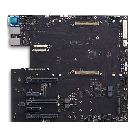
Page 14: Component Location
COM-HPC Server Base User’s Guide PICMG COM-HPC Rev 1.0 3. Component Location Figure 2 – Component location Page 14 Copyright © 2023 ADLINK Technology, Inc. -
Page 15: Functional Diagram
COM-HPC Server Base User’s Guide PICMG COM-HPC Rev 1.0 4. Functional Diagram Figure 3 – Functional diagram Page 15 Copyright © 2023 ADLINK Technology, Inc. -
Page 16: Mechanical Dimension
COM-HPC Server Base User’s Guide PICMG COM-HPC Rev 1.0 5. Mechanical Dimension Figure 4 – Mechanical dimensions Note: All dimensions are shown in millimeters with a tolerance of ± 0.25mm unless otherwise noted. Page 16 Copyright © 2023 ADLINK Technology, Inc. -
Page 17: Connectors And Pinouts
COM-HPC Server Base User’s Guide PICMG COM-HPC Rev 1.0 6. Connectors and Pinouts 6.1. Carrier Board Signals — Server Type Figure 5 – Carrier board signals, Server type pinout Page 17 Copyright © 2023 ADLINK Technology, Inc. -
Page 18: Connector Location And Pinout Compatibility
6.2. Connector Location and Pinout Compatibility Connector positions and pinouts comply with pinout and signal descriptions within PICMG COM-HPC Carrier Design Guide R2. This document includes: descriptions of pinouts, signals, and mechanical characteristics of the COM-HPC specification. The COM-HPC Server Base carrier is compatible with COM-HPC modules in Size E and D form factor, Server Type pinout, COM-HPC Module Base Specification R1.0. -
Page 19: Carrier Board Design
COM-HPC Server Base follows the PICMG COM-HPC Carrier Design Guide where possible, and its design and schematic have been fully verified. It is recommend to utilize them as references for your carrier board design. COM-HPC Server Base schematics and mechanical files, as well as the CDG, can be downloaded from ADLINK COM’s webpage. - Page 20 COM-HPC Server Base User’s Guide PICMG COM-HPC Rev 1.0 Row A Row B Row C Row D ETH5_RX- RSVD ETH1_TX- ETH1_RX+ ETH5_RX+ VCC_5V_SBY ETH1_TX+ USB67_OC# ETH2_RX- ETH6_RX- USB45_OC# ETH2_TX- ETH2_RX+ ETH6_RX+ USB23_OC# ETH2_TX+ USB01_OC# ETH3_RX- ETH7_RX- SML1_CLK ETH3_TX- ETH3_RX+ ETH7_RX+...
- Page 21 COM-HPC Server Base User’s Guide PICMG COM-HPC Rev 1.0 Row A Row B Row C Row D PCIe_BMC_TX+ PCIe_REFCLK0_LO+ PCIe08_RX- PCIe00_TX- PCIe08_TX- PCIe08_RX+ PCIe00_RX- PCIe00_TX+ PCIe08_TX+ PCIe00_RX+ PCIe09_RX- PCIe01_TX- PCIe09_TX- PCIe09_RX+ PCIe01_RX- PCIe01_TX+ PCIe09_TX+ PCIe01_RX+ PCIe10_RX- PCIe02_TX- PCIe10_TX- PCIe10_RX+ PCIe02_RX-...
- Page 22 COM-HPC Server Base User’s Guide PICMG COM-HPC Rev 1.0 Row A Row B Row C Row D GPIO_09 GPSPI_CS2# I2C1_DAT NBASET0_LINK_MAX# GPIO_10 GPSPI_CS3# NBASET0_SDP NBASET0_LINK_MID# GPIO_11 GPSPI_CLK NBASET0_CTREF NBASET0_LINK_ACT# A100 TYPE0 B100 GPSPI_ALERT# C100 TYPE1 D100 TYPE2 Row E Row F...
- Page 23 COM-HPC Server Base User’s Guide PICMG COM-HPC Rev 1.0 Row E Row F Row G Row H PCIe35_TX+ PCIe43_RX+ PCIe36_RX- PCIe44_TX- PCIe36_TX- PCIe36_RX+ PCIe44_RX- PCIe44_TX+ PCIe36_TX+ PCIe44_RX+ PCIe37_RX- PCIe45_TX- PCIe37_TX- PCIe37_RX+ PCIe45_RX- PCIe45_TX+ PCIe37_TX+ PCIe45_RX+ PCIe38_RX- PCIe46_TX- PCIe38_TX- PCIe38_RX+ PCIe46_RX-...
- Page 24 COM-HPC Server Base User’s Guide PICMG COM-HPC Rev 1.0 Row E Row F Row G Row H PCIe48_RX- PCIe56_TX- PCIe48_TX- PCIe48_RX+ PCIe56_RX- PCIe56_TX+ PCIe48_TX+ PCIe56_RX+ PCIe49_RX- PCIe57_TX- PCIe49_TX- PCIe49_RX+ PCIe57_RX- PCIe57_TX+ PCIe49_TX+ PCIe57_RX+ PCIe50_RX- PCIe58_TX- PCIe50_TX- PCIe50_RX+ PCIe58_RX- PCIe58_TX+ PCIe50_TX+...
-
Page 25: Pcie X16 Connectors
COM-HPC Server Base User’s Guide PICMG COM-HPC Rev 1.0 6.5. PCIe x16 Connectors CN5: PCIe x16 Slot1: Group 1 Lanes 16:31 assigned PCIe Slot CN6: PCIe x16 Slot2: Group 2 Lanes 32:47 assigned PCIe Slot CN7: PCIe x16 Slot3: Group 3 Lanes 48:63 assigned PCIe Slot... -
Page 26: Pcie X4 Connector
COM-HPC Server Base User’s Guide PICMG COM-HPC Rev 1.0 Pin Signal Pin Signal Pin Signal Pin Signal Pin Signal Pin Signal B64 GND A64 PERp11 B71 PETn13 A71 GND B78 PETp15 A78 GND B65 GND A65 PERn11 B72 GND A72 PERp13... -
Page 27: Key-M Slot Connector
COM-HPC Server Base User’s Guide PICMG COM-HPC Rev 1.0 6.7. KEY-M Slot Connector M2_0: Group 0 Lanes 8-11 assigned M.2 Slot 1 M2_1: Group 0 Lanes 12-15 assigned M.2 Slot 2 Pin Signal Pin Signal Pin Signal Pin Signal Pin Signal... -
Page 28: Usb2.0 Ports Header
COM-HPC Server Base User’s Guide PICMG COM-HPC Rev 1.0 6.8. USB2.0 Ports Header USB4_5: USB2.0 Port 4 and Port 5 header USB6_7: USB2.0 Port 6 and Port 7 header Pin Signal U2_USB_R_N U2_USB_R_N U2_USB_R_P U2_USB_R_P 6.9. USB3.x Ports Header FP_USB: USB Front Panel Header... -
Page 29: Sata Port
COM-HPC Server Base User’s Guide PICMG COM-HPC Rev 1.0 6.10. SATA Port SATA0/SATA1: Serial ATA Port Pin Signal TX_P TX_N RX_P RX_N SATA0_P7 JP_S0/JP_S1: Voltage supply switching for +3.3V or 5V for SATA DOM. Status +3.3V for SATA +5V for SATA... -
Page 30: Espi Debug Connector
COM-HPC Server Base User’s Guide PICMG COM-HPC Rev 1.0 6.11. eSPI Debug Connector ESPI: for eSPI debugging connection purpose Signal Signal eSPI_CLK eSPI_CS0 eSPI_RST RST_DBG_L eSPI_IO_3 eSPI_IO_1 + 3.3VSB eSPI_IO_1 eSPI_IO_0 SMB_CK CN_SNB_DAT BIOSRST eSPI_CS1# eSPI_ALEART0# eSPI_ALEART1# 6.12. BMC Debug Connector... -
Page 31: Com Port Connector
COM-HPC Server Base User’s Guide PICMG COM-HPC Rev 1.0 6.13. COM Port Connector COM1: the Module UART port1 Pin Signal CM1_DCD CN1_DSR SER1_RX SER1_RTS_L SER1_TX SER1_CTS_L CM1_DTR CM1_RI JP9: MUX of Module UART1 or BMC UART SOL Jumper Status BMC UART2 SOL <<<<... -
Page 32: I2C0/1 And Smbus Header
COM-HPC Server Base User’s Guide PICMG COM-HPC Rev 1.0 6.14. I2C0/1 and SMBus Header CN23: Module outputs I2C0/1 and SMBus external header Pin Signal Pin Signal +3.3V +3.3V SMB_CLK I2C0_CLK SMB_DAT I2C0_DAT +3.3V I2C0_ALERT-L I2C1_CLK I2C1_DAT 6.15. GPIO Header CN24: Module outputs GPIO Header... -
Page 33: External Smbus Header
COM-HPC Server Base User’s Guide PICMG COM-HPC Rev 1.0 6.16. External SMBus Header CN35: External SMBus for connecting to the MUX of KR/SFI Pin Signal RT_SDC RT_SDA 6.17. Fan Header FAN_0: Module controlled FAN Pin Signal +12V_5V_FAN SENSE_FAN PWMOUT_FAN FAN_1: BMC controlled FAN 1... - Page 34 COM-HPC Server Base User’s Guide PICMG COM-HPC Rev 1.0 FAN_2: BMC controlled FAN 2 Pin Signal +12V_5V_FAN1 SENSE_FAN1 PWMOUT_FAN1 FAN_4: BMC controlled FAN 4 Pin Signal +12V_5V_FAN3 SENSE_FAN3 PWMOUT_FAN3 FAN_5: BMC controlled FAN 5 Pin Signal +12V_5V_FAN4 SENSE_FAN4 PWMOUT_FAN4 Page 34...
-
Page 35: General Purpose Spi Header
COM-HPC Server Base User’s Guide PICMG COM-HPC Rev 1.0 6.18. General Purpose SPI Header GP_SPI: General Purpose SPI connector for widely used interfaces Pin Signal Pin Signal +3.3V GP_SPI_CLK GP_SPI_MOSI GP_SPI_CS2 GP_SPI_MISO GP_SPI_CS3 GP_SPI_CS0 GP_SPI_ALT GP_SPI_CS1 6.19. IPMI Header IPMI: Intelligent Platform Management Bus for platform management functions Pin Signal +3.3V... -
Page 36: Front Panel Control
COM-HPC Server Base User’s Guide PICMG COM-HPC Rev 1.0 6.20. Front Panel Control FRONT_PANEL: Power Button, Reset Button, HDD LED, Power LED for front panel header Signal Signal LAN2_LED_N NMI_SW LAN2_LED_P CASE_OPEN_N R_UID_BUT_P SENSOR_SCL SENSOR_SDA RST_BUT_P LAN1_LED_N LAN1_LED_P PWR_BUT_P SLED_R... -
Page 37: Power Connectors
COM-HPC Server Base User’s Guide PICMG COM-HPC Rev 1.0 6.21. Power Connectors ATX_24: ATX 24-pin Power Connector Connect the ATX 24-pin (or 20-pin) connector to supply power to COM-HPC Server Base carrier. Signal Signal +3.3V +3.3V +3.3V -12V PWR_ON PWR_GOOD... -
Page 38: Carrier Eeprom Address Switch
COM-HPC Server Base User’s Guide PICMG COM-HPC Rev 1.0 ATX_8: ATX 12V 8-pin Connector. Connect the ATX 12V 8-pin connector to supply power to the COM-HPC Server module. Signal +12V +12V +12V +12V 6.22. Carrier EEPROM Address Switch SW1: COM-HPC Carrier Board EEPROM address setting... -
Page 39: Module (I2C0) / Bmc (I2C8) Jumpers
COM-HPC Server Base User’s Guide PICMG COM-HPC Rev 1.0 6.23. Module (I2C0) / BMC (I2C8) Jumpers JP2: I2C CLK switch for I2C8 (BMC) or I2C0 (module) Jumper Status I2C8, BMC I2C0, Module JP3: I2C DAT switch for I2C8 (BMC) or I2C0 (module) -
Page 40: Power Jumpers
COM-HPC Server Base User’s Guide PICMG COM-HPC Rev 1.0 Setting Boot from Carrier BIOS JP29 JP28 JP27 BOOT Carrier BIOS <<<< JP30: Clear CMOS To clear CMOS, shut down the power and short pins 2 and 3 (short VBT to ground) - Page 41 COM-HPC Server Base User’s Guide PICMG COM-HPC Rev 1.0 JP32: ATX S3 signal switching In AT mode, put pin 2-3 for S5 output instead Power Button (S3) Jumper Status ATX (SUS_S3#) <<<< AT (SUS_S5#) JP33: VCC_12V On/Off during S3/S5 In AT mode, put pin 2-3 to output 12V during S3/S5.
-
Page 42: Secondary Bios
COM-HPC Server Base User’s Guide PICMG COM-HPC Rev 1.0 7. Secondary BIOS The COM-HPC Server-Base supports Secondary BIOS, using Boot Serial Peripheral Interface (SPI) for COM-HPC modules. Secondary BIOS solutions can be used as an alternative to the on-module BIOS and provide support for the following: •... -
Page 43: Switches, Post And Leds
COM-HPC Server Base User’s Guide PICMG COM-HPC Rev 1.0 8. Switches, POST and LEDs 8.1. Switches (S0-S5) There are two switches, at the center and lower-right of the carrier. PWR_BTN Indicates getting into S0 from S5 of the system. Page 43... - Page 44 COM-HPC Server Base User’s Guide PICMG COM-HPC Rev 1.0 RST_BTN Indicates resetting of the system. Page 44 Copyright © 2023 ADLINK Technology, Inc.
-
Page 45: Post And Inductors Leds
COM-HPC Server Base User’s Guide PICMG COM-HPC Rev 1.0 8.2. POST and inductors LEDs An eSPI-based POST display is added for debugging. The two 7-SEG LEDs shows the actual POST data. A row of mini-LEDs below the POST display indicates the following:... -
Page 46: Atx Power Connectors
COM-HPC Server Base User’s Guide PICMG COM-HPC Rev 1.0 8.3. ATX Power Connectors The COM-HPC Server Base has one ATX 24-pin connector to supply power to the carrier board and one ATX 12V 8-pin connector to supply power to the COM-HPC module. -
Page 47: At Power Mode
COM-HPC Server Base User’s Guide PICMG COM-HPC Rev 1.0 8.4. AT Power Mode To operate the system in AT Mode with an ATX power supply, Refer to section 6.24 jumper settings for details, or follow the instruction below. Jumper Settings for ATX mode...
Need help?
Do you have a question about the COM-HPC and is the answer not in the manual?
Questions and answers