
Related Manuals for ADLINK Technology arm AMPERE COM-HPC-ALT


Summary of Contents for ADLINK Technology arm AMPERE COM-HPC-ALT
- Page 1 Express-ID7 User’s Guide PICMG COM.0 R3.1 COM-HPC-ALT User’s Guide Revision: Rev. 0.1 Date: 2023-01-10 Part Number: 50M-00115-1000 Page 1 Copyright © 2023 ADLINK Technology, Inc.
-
Page 2: Revision History
COM-HPC-ALT User’s Guide PICMG COM-HPC R1.0 Revision History Revision Description Date Author Preliminary release 2023-01-10 Page 2 Copyright © 2023 ADLINK Technology, Inc. -
Page 3: Preface
Product names mentioned herein are used for identification purposes only and may be trademarks / registered trademarks of respective companies. Copyright © 2023 ADLINK Technology Incorporated This document contains proprietary information protected by copyright. All rights are reserved. No part of this manual may be reproduced by any mechanical, electronic, or other means in any form without prior written permission of the manufacturer. - Page 4 Only install/attach and operate equipment on stable surfaces and/or recommended mountings; • If the equipment will not be used for long periods of time, turn off the power source and unplug the equipment. • Page 4 Copyright © 2023 ADLINK Technology, Inc.
- Page 5 Caution: This information indicates the possibility of minor physical injury, component damage, data loss, and/or program corruption. Warning: This information warns of possible serious physical injury, component damage, data loss, and/or program corruption. Page 5 Copyright © 2023 ADLINK Technology, Inc.
- Page 6 ADLINK Technology GmbH Hans-Thoma-Strasse 11, D-68163 Mannheim, Germany Tel: +49-621-43214-0 Fax: +49-621 43214-30 Email: emea@adlinktech.com Please visit the Contact page at www.adlinktech.com for information on how to contact the ADLINK regional office nearest you. Page 6 Copyright © 2023 ADLINK Technology, Inc.
-
Page 8: Table Of Contents
4.3.7 Port 80 Support on USB_PD I2C Bus ......................................................22 4.3.8 IPMB ..................................................................22 4.3.9 General Purpose SPI ............................................................23 4.3.10 Power & System Management ........................................................24 4.3.11 Thermal Protection ............................................................25 Page 0 Copyright © 2023 ADLINK Technology, Inc. - Page 9 Thermal Solutions ................................................................ 40 7.2.1 Heatsink : THS-ALT-BL ........................................................... 40 7.2.2 Low profile active cooler: THSF-ALT-BL-S ....................................................41 7.2.3 High profile passive heatsink: THSH-ALT-VC ..................................................42 7.2.4 Active Cooling: THSF-ALT-BL ........................................................43 Page 1 Copyright © 2023 ADLINK Technology, Inc.
- Page 10 Figure 2 – Module Rear Side Row ......................................................21 Figure 4 – Heatsink THS-ALT-BL ....................................................... 40 Figure 5 – THSF-ALT-BL-S ........................................................... 41 Figure 6 – High profile passive heatsink THSH-ALT-VC ..............................................42 Figure 7 – Cooler THSF-ALT-BL ......................................................... 43 Page 2 Copyright © 2023 ADLINK Technology, Inc.
-
Page 11: Introduction
One security chip is supported on the module. The traditional TPM 2.0, SPI based (same as Ampere Altra reference design) (it is on GP_SPI bus) The module is equipped with EDK2 (bootloader, open source) BIOS with CMOS backup, supporting embedded features such as remote console, hardware monitor, and watchdog timer. No EC on this product. Page 3 Copyright © 2023 ADLINK Technology, Inc. -
Page 12: Specifications
Ampere Computing, Ampere® Altra® Series Processors • M128-26 128 cores, 2.6GHz, 190W TDP • Q80-26 80 cores, 2.6GHz, 150W TDP • Q64-22 64 cores, 2.2GHz, 95W TDP • Q32-17 32 cores, 1,7GHz, 65W TDP Page 4 Copyright © 2023 ADLINK Technology, Inc. -
Page 13: Expansion Busses
1 x16 or 2 x8 or 4 x4 config at 32-47, (from Root Complex A) PCIe 48-63 1 x16 or 2 x8 or 4 x4 config at 48-63, (from Root Complex A) Page 5 Copyright © 2023 ADLINK Technology, Inc. - Page 14 Support 3.3V of VCC_BOOT_SPI pin, if SPI flash on carrier is implemented, it shall be powered by VCC_BOOT_SPI pin BIOS Boot Selection BIOS flash can be boot up at SPI bus, can be located at module or carrier or combined Page 6 Copyright © 2023 ADLINK Technology, Inc.
- Page 15 MMC and Carrier BMC through IPMB. A dedicated PCIe x1 lane is also available on the Carrier BMC, allowing the Carrier BMC to generate a VGA or other format video output, for management functions. Page 7 Copyright © 2023 ADLINK Technology, Inc.
-
Page 16: Ethernet
Supports Wake on LAN at S3/S4/S5 Supports PXE boot Ethernet KR/KX Interfaces Broadcom® Ethernet Controller BCM57502, connected to the SoC through PCIex8 lane 4x 10GBASE-KR and its sideband signals Supports both full-duplex and half-duplex Page 8 Copyright © 2023 ADLINK Technology, Inc. -
Page 17: Multi I/O And Storage
Note: UART0, 1 both source from SOC. UART0 offers TX, RX, RTS#, CTS#. UART1 only offers TX and RX; its RTS#, CTS# are simulated by 2 GPIO from SOC. GPIO 12x GPIO Supports GPI with interrupt Page 9 Copyright © 2023 ADLINK Technology, Inc. -
Page 18: Others
8-10 voltage are monitored by EC, customer can get voltage information on BIOS menu and also shown in SEMA GUI and access it through SEMA API 2.6 Security This module offers one security-related chip on the module. Page 10 Copyright © 2023 ADLINK Technology, Inc. -
Page 19: Module Management Controller (Mmc)
CPU / SOC, DRAM memory, an internal display controller and more. It may be ARM based. It may run a Linux or other OS. A popular vendor for this sort of BMC part is Aspeed, and in particular the Aspeed AST2510 and successor parts. Many other vendors and parts are possible. Page 11 Copyright © 2023 ADLINK Technology, Inc. - Page 20 The MMC, if implemented, shall include an IPMB slave interface. It may additionally interface to the Carrier BMC over any of several other COM-HPC interfaces, including the I2C0 and or UART0 ports. Page 12 Copyright © 2023 ADLINK Technology, Inc.
- Page 21 (size A, B, C or size D,E) then a C.U or C.M Carrier shall be basically operable with a M.U or M.B or M.F Module. The OOB management features may be missing, depending on what is matched with what. Additionally, there will likely be some vendor specific aspects to OOB management options. Page 13 Copyright © 2023 ADLINK Technology, Inc.
- Page 22 COM-HPC-ALT User’s Guide PICMG COM-HPC R1.0 M.B Module and C.M Carrier will be implemented at ADLINK COM-HPC Server Module and COM-HPC Server Carrier as first wave. IPMI on COM-HPC Page 14 Copyright © 2023 ADLINK Technology, Inc.
- Page 23 The EEPROM area for storing EeeP data may be implemented as a physical EEPROM on the board, on the I2C0 bus. Alternatively, it may be realized within the MMC. This is illustrated in Figure 10 above. In that figure, it is labeled as an “emulated EEPROM”. An I2C slave interface on the MMC is Page 15 Copyright © 2023 ADLINK Technology, Inc.
- Page 24 The Module EEPROM I2C device address lines, A2, A1 and A0 shall be pulled to a logic low, placing the device at address 0x50 (7 bit I2C addressing) and address 0xA0(8 bit I2C addressing). Note: I2C address A6-A3 are fixed at 1010b for I2C EEPROM devices per the I2C specification. Page 16 Copyright © 2023 ADLINK Technology, Inc.
-
Page 25: Debug
AT 12V±5% Power Management: ACPI 5.0 compliant, Smart Battery support Power States: C1-C6, S0, S1, S5, S5 ECO mode (Wake-on-USB, WoL S5) ECO Mode support for deep S5 for 5Vsb power saving Page 17 Copyright © 2023 ADLINK Technology, Inc. -
Page 26: Mechanical And Environmental
IEC 60068-2-64 and IEC-60068-2-27 MIL-STD-202F, Method 213B, Table 213-I, Condition A and Method 214A, Table 214-I, Condition D HALT tested Thermal Stress, Vibration Stress, Thermal Shock and Combined Test EN55032 Class B inside an enclosure Page 18 Copyright © 2023 ADLINK Technology, Inc. - Page 27 MTBF 200,000 hrs commercial 40℃ ambient (according MIL calculation) based on actual calculated de-rating 120,000 hrs ETT -20℃~70℃ ambient (according MIL calculation) based on actual calculated de-rating (excludes the BCM57504 LAN controller) Page 19 Copyright © 2023 ADLINK Technology, Inc.
-
Page 28: Block Diagram
-UART_1: TX, RX come from SOC, RTS#, CTS# are simulated by SOC GPIO -USB_PD_I2C, MMC, SOC: connect together -need work with AST2500 Remote BMC on carrier Figure 1 – Module Function Block Diagram Page 20 Copyright © 2023 ADLINK Technology, Inc. -
Page 29: Pinout And Signal Descriptions
PICMG COM-HPC Rev 1.0 specification. Signals described in the specification but not supported on the COM-HPC-ALT are marked by strikethrough ROW A/B/C/D on J1 connector, ROW E/F/G/H on J2 connector Figure 2 – Module Rear Side Row Page 21 Copyright © 2023 ADLINK Technology, Inc. - Page 30 ETH2_TX- ETH2_RX+ ETH6_RX+ USB23_OC# ETH2_TX+ USB01_OC# ETH3_RX- ETH7_RX- SML1_CLK ETH3_TX- ETH3_RX+ ETH7_RX+ SML1_DAT ETH3_TX+ PMCALERT# USB3_SSTX- RSVD SML0_CLK USB3_SSRX- USB3_SSTX+ RSVD SML0_DAT USB3_SSRX+ USB_PD_ALERT# USB2_SSTX- ETH4_TX- USB_PD_I2C_CLK USB2_SSRX- USB2_SSTX+ ETH4_TX+ USB_PD_I2C_DAT USB2_SSRX+ Page 1 Copyright © 2023 ADLINK Technology, Inc.
- Page 31 PCIe08_RX- PCIe00_TX- PCIe08_TX- PCIe08_RX+ PCIe00_RX- PCIe00_TX+ PCIe08_TX+ PCIe00_RX+ PCIe09_RX- PCIe01_TX- PCIe09_TX- PCIe09_RX+ PCIe01_RX- PCIe01_TX+ PCIe09_TX+ PCIe01_RX+ PCIe10_RX- PCIe02_TX- PCIe10_TX- PCIe10_RX+ PCIe02_RX- PCIe02_TX+ PCIe10_TX+ PCIe02_RX+ PCIe11_RX- PCIe03_TX- PCIe11_TX- PCIe11_RX+ PCIe03_RX- PCIe03_TX+ PCIe11_TX+ PCIe03_RX+ Page 2 Copyright © 2023 ADLINK Technology, Inc.
- Page 32 I2C0_CLK GPIO_06 GPSPI_MISO I2C0_DAT NBASET0_MDI3- GPIO_07 GPSPI_CS0# I2C0_ALERT# NBASET0_MDI3+ GPIO_08 GPSPI_CS1# I2C1_CLK GPIO_09 GPSPI_CS2# I2C1_DAT NBASET0_LINK_MAX# GPIO_10 GPSPI_CS3# NBASET0_SDP NBASET0_LINK_MID# GPIO_11 GPSPI_CLK NBASET0_CTREF NBASET0_LINK_ACT# A100 TYPE0 B100 GPSPI_ALERT# C100 TYPE1 D100 TYPE2 Page 3 Copyright © 2023 ADLINK Technology, Inc.
- Page 33 PCIe33_TX+ PCIe41_RX+ PCIe34_RX- PCIe42_TX- PCIe34_TX- PCIe34_RX+ PCIe42_RX- PCIe42_TX+ PCIe34_TX+ PCIe42_RX+ PCIe35_RX- PCIe43_TX- PCIe35_TX- PCIe35_RX+ PCIe43_RX- PCIe43_TX+ PCIe35_TX+ PCIe43_RX+ PCIe36_RX- PCIe44_TX- PCIe36_TX- PCIe36_RX+ PCIe44_RX- PCIe44_TX+ PCIe36_TX+ PCIe44_RX+ PCIe37_RX- PCIe45_TX- PCIe37_TX- PCIe37_RX+ PCIe45_RX- PCIe45_TX+ Page 4 Copyright © 2023 ADLINK Technology, Inc.
- Page 34 PCIe21_TX+ PCIe29_RX+ PCIe22_RX- PCIe30_TX- PCIe22_TX- PCIe22_RX+ PCIe30_RX- PCIe30_TX+ PCIe22_TX+ PCIe30_RX+ PCIe23_RX- PCIe31_TX- PCIe23_TX- PCIe23_RX+ PCIe31_RX- PCIe31_TX+ PCIe23_TX+ PCIe31_RX+ PCIe48_RX- PCIe56_TX- PCIe48_TX- PCIe48_RX+ PCIe56_RX- PCIe56_TX+ PCIe48_TX+ PCIe56_RX+ PCIe49_RX- PCIe57_TX- PCIe49_TX- PCIe49_RX+ PCIe57_RX- PCIe57_TX+ Page 5 Copyright © 2023 ADLINK Technology, Inc.
- Page 35 E100 PCIe_PERST_IN0# F100 PCIe_PERST_IN1# G100 PCIe_WAKE_OUT0# H100 PCIe_WAKE_OUT1# Note: Strikethrough entries are functions not supported by this product. IPMB is supported if there’s MMC on module. No eSPI support on this platform Page 6 Copyright © 2023 ADLINK Technology, Inc.
-
Page 36: Signal Terminology Descriptions
Pull-down strap. A Module output pin that is either tied to GND or is not connected. Used to signal Module capabilities to the Carrier Board. PU (pull-up) resistor on module PD (pull-down) resistor on module Page 7 Copyright © 2023 ADLINK Technology, Inc. -
Page 37: Signal Descriptions On J1/J2 Connectors
3.3VSB MAC and an external PHY for ETHx ports 0 to 3 ETH0-3_INT# Active low interrupt signal from IO Port expanders for PU 2K2 ETH ports 0 to 3 3.3VSB Page 8 Copyright © 2023 ADLINK Technology, Inc. -
Page 38: Nbase-T Ethernet
PU / PD Comment NBASET0_MDI0- Ethernet Controller 1: Media Dependent Interface Differential Pairs I/O Analog Twisted pair signals for external transformer. 0,1,2,3. The MDI can operate in 10Gbps, 1Gbps, 100Mbps and 10 Page 9 Copyright © 2023 ADLINK Technology, Inc. - Page 39 Module. In the case in which the reference is shorted to ground, the current shall be limited to 250 mA or less. NBASET0_SDP NBASE-T Ethernet Controller 0 Software-Definable Pin. Can also be IO 3.3VSB used for IEEE1588 support such as a 1pps signal. Page 10 Copyright © 2023 ADLINK Technology, Inc.
-
Page 40: Pci Express
PCIe01_RX+ PCIe01_RX- PCIe02_RX+ PCIe02_RX- PCIe03_RX+ PCIe03_RX- PCIe04_RX+ PCIe04_RX- PCIe05_RX+ PCIe05_RX- PCIe06_RX+ PCIe06_RX- PCIe07_RX+ PCIe07_RX- PCIe08_TX+ PCI Express Differential Transmit Pairs 8-15 O PCIe AC coupled on Module PCIe08_TX- PCIe Group 0 High Page 11 Copyright © 2023 ADLINK Technology, Inc. - Page 41 PCIe12_RX+ PCIe12_RX- PCIe13_RX+ PCIe13_RX- PCIe14_RX+ PCIe14_RX- PCIe15_RX+ PCIe15_RX- PCIe16_TX+ PCI Express Differential Transmit Pairs 16-31 O PCIe AC coupled on Module PCIe16_TX- PCIe Group 1 PCIe17_TX+ PCIe17_TX- PCIe18_TX+ PCIe18_TX- PCIe19_TX+ PCIe19_TX- PCIe20_TX+ Page 12 Copyright © 2023 ADLINK Technology, Inc.
- Page 42 PCIe31_TX- PCIe16_RX+ PCI Express Differential Receive Pairs 16-31 I PCIe AC coupled off Module PCIe16_RX- PCIe Group 1 PCIe17_RX+ PCIe17_RX- PCIe18_RX+ PCIe18_RX- PCIe19_RX+ PCIe19_RX- PCIe20_RX+ PCIe20_RX- PCIe21_RX+ PCIe21_RX- PCIe22_RX+ PCIe22_RX- PCIe23_RX+ PCIe23_RX- Page 13 Copyright © 2023 ADLINK Technology, Inc.
- Page 43 PCI Express Differential Transmit Pairs 32-47 O PCIe AC coupled on Module PCIe32_TX- PCIe Group 2 PCIe33_TX+ PCIe33_TX- PCIe34_TX+ PCIe34_TX- PCIe35_TX+ PCIe35_TX- PCIe36_TX+ PCIe36_TX- PCIe37_TX+ PCIe37_TX- PCIe38_TX+ PCIe38_TX- PCIe39_TX+ PCIe39_TX- PCIe40_TX+ PCIe40_TX- PCIe41_TX+ PCIe41_TX- PCIe42_TX+ PCIe42_TX- PCIe43_TX+ Page 14 Copyright © 2023 ADLINK Technology, Inc.
- Page 44 PCIe32_RX- PCIe Group 2 PCIe33_RX+ PCIe33_RX- PCIe34_RX+ PCIe34_RX- PCIe35_RX+ PCIe35_RX- PCIe36_RX+ PCIe36_RX- PCIe37_RX+ PCIe37_RX- PCIe38_RX+ PCIe38_RX- PCIe39_RX+ PCIe39_RX- PCIe40_RX+ PCIe40_RX- PCIe41_RX+ PCIe41_RX- PCIe42_RX+ PCIe42_RX- PCIe43_RX+ PCIe43_RX- PCIe44_RX+ PCIe44_RX- PCIe45_RX+ PCIe45_RX- PCIe46_RX+ PCIe46_RX- Page 15 Copyright © 2023 ADLINK Technology, Inc.
- Page 45 PCIe57_TX- PCIe58_TX+ PCIe58_TX- PCIe59_TX+ PCIe59_TX- PCIe60_TX+ PCIe60_TX- PCIe61_TX+ PCIe61_TX- PCIe62_TX+ PCIe62_TX- PCIe63_TX+ PCIe63_TX- PCIe48_RX+ PCI Express Differential Receive Pairs 48-63 I PCIe AC coupled off Module PCIe48_RX- PCIe Group 3 PCIe49_RX+ PCIe49_RX- Page 16 Copyright © 2023 ADLINK Technology, Inc.
- Page 46 Reference clock pair for PCIe lanes [0:7], also referred O PCIe PCIe_REFCLK0_LO+ to PCIe Group 0 Low and for the PCIe_BMC link PCIe_REFCLK0_HI- Reference clock pair for PCIe lanes [8:15], also O PCIe PCIe_REFCLK0_HI+ referred to PCIe Group 0 High Page 17 Copyright © 2023 ADLINK Technology, Inc.
-
Page 47: Usb
USB0 may be configured as a USB client or as a host, This product only support USB0-3 through a PCIe to USB IC USB1- or both at the Module designer's discretion. All other USB2+ USB ports, if implemented, shall be host ports. Page 18 Copyright © 2023 ADLINK Technology, Inc. - Page 48 I PCIe AC coupled off Module USB2_SSRX- USB 3.2 Gen 1 or Gen 2 implementations. USB3_SSRX+ This product only support USB0-3 (up to USB 3.2 Gen1) USB3_SSRX- through a PCIe to USB IC Page 19 Copyright © 2023 ADLINK Technology, Inc.
-
Page 49: Asynchronous Serial Port
It is preferred that if the Module is based on an Intel x86 architecture, the Module serial ports be I/O mapped and be register compatible with the National Semiconductor 16550 UARTs that were used in the PC AT architecture. Page 20 Copyright © 2023 ADLINK Technology, Inc. -
Page 50: I2C
400KHz operation. The ports should be multi-master capable. I2C0 is defined to operate from a 3.3V rail and I2C1 from a 1.8V rail. The I2C1 port may be I3C capable. I2C source from Ampere Altra SOC supports multi-master Page 21 Copyright © 2023 ADLINK Technology, Inc. -
Page 51: Port 80 Support On Usb_Pd I2C Bus
An IPMB (Intelligent Platform Management Bus) port is defined for both the Client and Server pinout types for platform management functions. The IPMB is used (optionally) with a Carrier based BMC (Board Management Controller) Master. On the Module, the IPMB should be routed to and used Page 22 Copyright © 2023 ADLINK Technology, Inc. -
Page 52: General Purpose Spi
Serial data from the COM-HPC Module to the Carrier O 3.3V GP_SPI device (“Master Out Slave In”) GP_SPI_CLK Clock from the Module to Carrier GP_SPI device O 3.3V GP_SPI_CS0# GP_SPI chip selects, active low O 3.3V GP_SPI_CS1# GP_SPI_CS2# GP_SPI_CS3# Page 23 Copyright © 2023 ADLINK Technology, Inc. -
Page 53: Power & System Management
Even in single input supply system implementations (AT mode, no standby input), the SUS_S3# Module output should be used disable any Carrier voltage regulators when SUS_S3# is low, to prevent bleed leakage from Carrier circuits into the Module. Page 24 Copyright © 2023 ADLINK Technology, Inc. -
Page 54: Thermal Protection
PU / PD Comment CARRIER_HOT# Input from off-Module temp sensor indicating an I 3.3V PU 4.7K over-temp situation. THERMTRIP# Active low output indicating that the CPU has entered O 3.3V thermal shutdown. Page 25 Copyright © 2023 ADLINK Technology, Inc. -
Page 55: Smbus
3.3VSB 3.3VSB GPIO_02 inputs. GPIO_03 GPIO_04 As inputs, these pins should be able to generate an GPIO_05 interrupt to the Module host. GPIO_06 GPIO_07 GPIO_08 GPIO_09 GPIO_10 GPIO_11 Page 26 Copyright © 2023 ADLINK Technology, Inc. -
Page 56: Module Type Definition
VCC to the COM-HPC Module) if an incompatible Module pin-out type is detected. All three TYPE[x] pins should be monitored by the Carrier. The Carrier Board logic may also implement a fault indicator such as an LED. Page 27 Copyright © 2023 ADLINK Technology, Inc. -
Page 57: Miscellaneous Signals
The selection of the output modes may be realized by software configurable hardware or by Module build options. WD Mode Description Comment The Module generates an internal reset. Module output pin PLTRST# is driven low. The WD_OUT pin is driven high until the unit resets. Page 28 Copyright © 2023 ADLINK Technology, Inc. - Page 58 The Strobe Interval shall be software programmable. Recommended ranges in enable delay and max strobe periods are given in the following table. Min Value Max Value Enable Delay 1 second 10 minutes Strobe Interval 0.1 second 10 minutes Page 29 Copyright © 2023 ADLINK Technology, Inc.
-
Page 59: Power And Ground
Real-time clock circuit-power input. Nominally +3.0V. Ground - DC power and signal and AC signal return path. All available GND connector pins shall be used and tied to Carrier Board GND plane(s). Page 30 Copyright © 2023 ADLINK Technology, Inc. -
Page 60: Additional Features
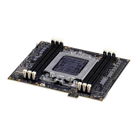
This chapter describes the connectors, LEDs, and switches, located on the module and are not necessarily included in the PICMG standard specification. The locations of these parts are as shown below: BIOS Default 40-pin Fan Connector Reset Debug Connect Page 31 Copyright © 2023 ADLINK Technology, Inc. -
Page 61: Debug Connector (40-Pin Connector)
This connector is particular useful during carrier design and bring up phase. It offers access to the following critical parts of the module: Test points for measurement of internal power rails • SPI BIOS programming interface • I2C bus for BIOS POST code readout • BMC programming interface • Page 32 Copyright © 2023 ADLINK Technology, Inc. -
Page 62: Status Leds
Rebooted after PWRBTN WD LED = LED OFF Rebooted after RESET BTN WD LED = LED OFF Note: only a Reset not initiated by the BMC can clear the WD LED (user action) Page 33 Copyright © 2023 ADLINK Technology, Inc. -
Page 63: Fan Connector
If the module’s input voltage is from 12V to 20V, the supply voltage will be 12V (± 5%) and the maximum supply current of the fan connector • will be TBC mA.. Page 34 Copyright © 2023 ADLINK Technology, Inc. -
Page 64: Bios Default Reset
2. Hold down the BIOS Setup Defaults Reset Button continuously and boot up the system. You can release the button when the BIOS prompt screen appears. 3. The BIOS prompt screen will display a confirmation that BIOS defaults have been reset and request that you reboot the system. Page 35 Copyright © 2023 ADLINK Technology, Inc. -
Page 65: Bios Boot Select
In either mode, BIOS Select and Mode Configuration Switch, Pin 1 is used to select whether to boot from SPI0 or SPI1. Mode Pin 1 Pin 2 Boot from SPI0 (default) Boot from SPI1 Set BIOS to PICMG mode (default, TBC) Set BIOS to Failsafe BIOS mode Page 36 Copyright © 2023 ADLINK Technology, Inc. -
Page 66: Bios Checkpoints, Beep Codes
• Driver Execution Environment (DXE) – main hardware initialization • Boot Device Selection (BDS) – system setup, pre-OS user interface & selecting a bootable device (CD/DVD, HDD, USB, Network, Shell, ...) • Page 37 Copyright © 2023 ADLINK Technology, Inc. -
Page 67: Status Code Ranges
0xE0 – 0xE8 S3 Resume (PEI) 0xE9 – 0xEF S3 Resume errors (PEI) 0xF0 – 0xF8 Recovery (PEI) 0xF9 – 0xFF Recovery errors (PEI) Note: Table above is subject to future updates. Page 38 Copyright © 2023 ADLINK Technology, Inc. -
Page 68: Mechanical And Thermal
COM-HPC-ALT User’s Guide PICMG COM-HPC R1.0 7. Mechanical and Thermal 7.1 Module Dimensions Module D Figure 3 – imensions (mm) Page 39 Copyright © 2023 ADLINK Technology, Inc. -
Page 69: Thermal Solutions
COM-HPC-ALT User’s Guide PICMG COM-HPC R1.0 Thermal Solutions 7.2.1 Heatsink : THS-ALT-BL Figure 4 – Heatsink THS-ALT-BL Page 40 Copyright © 2023 ADLINK Technology, Inc. -
Page 70: Low Profile Active Cooler: Thsf-Alt-Bl-S
COM-HPC-ALT User’s Guide PICMG COM-HPC R1.0 7.2.2 Low profile active cooler: THSF-ALT-BL-S Figure 5 – THSF-ALT-BL-S Page 41 Copyright © 2023 ADLINK Technology, Inc. -
Page 71: High Profile Passive Heatsink: Thsh-Alt-Vc
COM-HPC-ALT User’s Guide PICMG COM-HPC R1.0 7.2.3 High profile passive heatsink: THSH-ALT-VC Figure 6 – High profile passive heatsink THSH-ALT-VC Page 42 Copyright © 2023 ADLINK Technology, Inc. -
Page 72: Active Cooling: Thsf-Alt-Bl
COM-HPC-ALT User’s Guide PICMG COM-HPC R1.0 7.2.4 Active Cooling: THSF-ALT-BL Figure 7 – Cooler THSF-ALT-BL Page 43 Copyright © 2023 ADLINK Technology, Inc.
Need help?
Do you have a question about the arm AMPERE COM-HPC-ALT and is the answer not in the manual?
Questions and answers