Table of Contents
Advertisement
Quick Links
Advertisement
Table of Contents

Related Manuals for ADLINK Technology aTCA-6890


Summary of Contents for ADLINK Technology aTCA-6890
- Page 1 Intel® Xeon-based AdvancedTCA Processor Blade User’s Manual Manual Rev. 2.03 Revision Date: November 22, 2006 Part No: 50-1G001-1010 Advance Technologies; Automate the World. This datasheet has been downloaded from http://www.digchip.com at this page...
- Page 2 Copyright 2005 ADLINK TECHNOLOGY INC. All Rights Reserved. The information in this document is subject to change without prior notice in order to improve reliability, design, and function and does not represent a commitment on the part of the manufacturer.
- Page 3 Getting Service from ADLINK Customer Satisfaction is top priority for ADLINK Technology Inc. Please contact us should you require any service or assistance. ADLINK TECHNOLOGY INC. Web Site: http://www.adlinktech.com Sales & Service: Service@adlinktech.com TEL: +886-2-82265877 FAX: +886-2-82265717 Address: 9F, No. 166, Jian Yi Road, Chungho City,...
-
Page 5: Table Of Contents
Super I/O ................ 9 IPMI Controller ..............9 EIDE Interface ..............9 CMOS Battery ............... 10 aTCA-6890 Mechanical Layout ......... 11 aTCA-6890 Board Layout ..........11 Front Panel LED Indicators and Reset ......12 Unpacking Checklist ............13 2 Connectors and Jumpers ..........15 Connector Pin Assignments .......... - Page 6 Zone 1 Connector ............19 Zone 2-J23 Pin Assignment (PICMG 3.1 Option1) ..20 Zone 3 Pin Assignment ..........22 PMC Connectors ............23 Jumper Settings ..............27 Clear CMOS Jumper (SWZ1) ........27 3 Getting Started ..............29 CPU Installation ..............29 Memory Installation............
- Page 7 FRU States ................ 61 6 IPMC .................. 61 IPMC Overview..............61 FRU States ................ 61 Accessing the IPMC ............65 IPMI Command Set ............67 Sensor Data Record List............ 69 FRU Storage Information........... 70 Firmware/FRU EEPROM Update ........73 Update Procedures ............73 Misc.
-
Page 8: List Of Tables
List of Tables Table 1-1: CPUs Validated for the ATCA-6890 ......5 Table 1-2: SMB Address Functionality ........6 Table 1-3: PCI Express Configuration ........7 Table 1-4: Fabric Interface Options ........... 7 Table 1-5: LED Indicator Legend ..........12 Table 1-6: Base &... - Page 9 List of Figures Figure 1-1: aTCA 6890 Functional Block Diagram ...... 2 Figure 1-2: aTCA-6890 Board Layout........11 Figure 1-3: Front Panel .............. 12 Figure 3-1: Apply thermal grease to CPU(s)......29 Figure 3-2: CPU Installation............30 Figure 3-3: Apply thermal pad to outside edge of the CPU ..31 Figure 3-4: Memory slot locations..........
-
Page 11: Introduction
Introduction 1.1 Product Overview The aTCA-6890 is the dual 64bit Intel® LV-Xeon processor based AdvancedTCA blade. It supports Intel® EM64T 64-bit technology and dual channel DDR2-400 REG/ECC system memory up to 16GB capacity. For data transport connectivity, it features dual... -
Page 12: Figure 1-1: Atca 6890 Functional Block Diagram
Please refer to the following block diagram for the aTCA-6890 architecture. Figure 1-1: aTCA 6890 Functional Block Diagram Introduction... -
Page 13: Features
1.2 Features The features of the aTCA-6890 are as follows: 800MHz FSB 1MB L2 Cache Hyper-Threading Processors Intel® EM64T 64-bit Extended Memory Technology Dual DDR2-400 REG/ECC Channels with 16GB Maximum Capacity Intel® E7520/6300ESB/6700PXH Chipset Dual 64-bit 33/66/100/133MHz PCI/PCI-X PMC with PIM Quad 1000BASE-BX GbE Fabric Interface Channels Configurable PICMG 3.1 Option1/2 Compliant... - Page 14 USB: Dual USB v2.0 ports Front Panel I/Os: PMC1/2, VGA, USB1/2, LAN1/2, COM1 Standards PICMG 3.0 R2.0 ECN001 PICMG 3.1 Ethernet over PICMG 3.0, R1.0 Option 1/2 Introduction...
-
Page 15: Main Functions
Xeon processors might cause damage to the aTCA-6890 or processor. When using dual processors both processors must be the same S-Spec number. The aTCA-6890 is designed to be used with ADLINK’s thermal solution. Do not attempt to use the thermal solution provided in some of the boxed processor packages. -
Page 16: Pci Express
The memory controller supports two channels of memory, Channel A and Channel B. Each channel contains two SIMM sockets for a total of 4 DIMM sockets. The aTCA-6890 can be populated with one, two or four DIMM modules. When only one DIMM is used, it can be populated on either DDRII-A2 or DDRII-B2 socket. -
Page 17: Base Interface
3.1, Option 2, which configures the four GbE ports to Port0-1 of Fabric Interface Channel 1-2 (FCH[1:2]P[0:1]). As shipped, the aTCA-6890 is configured to operate in the PICMG 3.1 Option 1 mode. Refer to the table below for details. PICMG 3.1 Option... -
Page 18: Video
Video The video interface is provided with a ATI Rage XL video control- ler. The video controller is on a 32 bit 33MHz PCI bus. Video mem- ory of 8M bytes is available with resolutions up to QXGA (2048 x 1536). -
Page 19: Super I/O
The controller is provided for software compatibility reasons only. The PS/2 keyboard and mouse interfaces are routed to Zone 3 for use with the aTCA-6890 RTM. IPMI Controller The IPMI controller is based on the Pigeon Point Systems IPMC. It is fully compliant with the aTCA specification. -
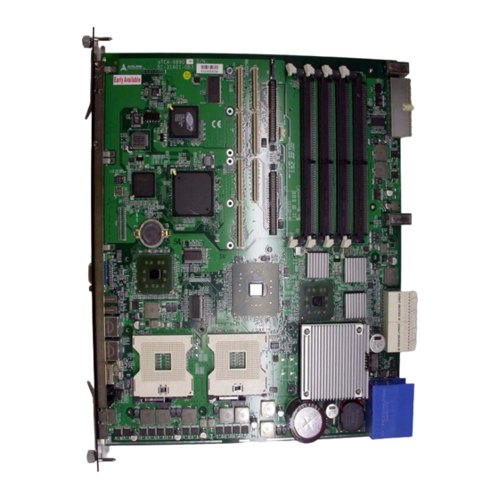
Page 20: Atca-6890 Mechanical Layout
1.4 aTCA-6890 Mechanical Layout aTCA-6890 Board Layout Figure 1-2: aTCA-6890 Board Layout Introduction... -
Page 21: Front Panel Led Indicators And Reset
Front Panel LED Indicators and Reset Front panel LEDs provide feedback to the user on the state of the aTCA-6890. A front panel reset switch is provided to allow a hard reset of the board. Color Function Out Of Service:... -
Page 22: Unpacking Checklist
Check the following items are included in the package, if there are any items missing, please contact your dealer: Included Items aTCA-6890 processor blade (CPU, RAM, and hard drive specifications will differ depending on options selected) Heat sink IDE HDD mounting kit... -
Page 23: Connectors And Jumpers
2.1 Connector Pin Assignments Detailed descriptions and pin-outs for each connector are given in the following section. Please refer to Figure 1-2: aTCA-6890 Board Board Layout and Figure 1-3: aTCA-6890 Front Panel for connector locations. Serial Port (COM1)) -
Page 24: Lan Rj-45 Connector (Lan1, Lan2)
LAN RJ-45 Connector (LAN1, LAN2) Signal Function green MDX0+ Pair 0 MDX0- MDX1+ Pair 1 MDX1- MDX2+ Pair 2 MDX2- MDX3+ yellow Pair 3 MDX3- LED Color Status Function 1000Mbps Green (speed) 100Mbps Link Yellow (link) Link off blinking Data transfer in progress USB Connector (Port 0, Port 1) SIGNAL USB-... -
Page 25: Vga Connector (Front Panel)
VGA Connector (Front Panel) Pin Signal Name Pin Signal Name Green Blue DDCDAT HSYNC VSYNC DDCLK — — Video Signal Definitions: Red signal Green signal Blue signal HSYNC Horizontal synchronization VSYNC Vertical synchronization DDCCLK Display Data Channel clock signal for DDC2 support DDCDAT Display Data Channel data signal for DDC2... -
Page 26: Ide Connectors (Cn2, Cn3)
IDE Connectors (CN2, CN3) Signal Signal RESET# Ground DD10 DD11 DD12 DD13 DD14 DD15 Ground N.C (key pin) DMARQ Ground DIOW# Ground DIOR# Ground IORDY CSEL DMACK# Ground INTRQ PDIAG# CS0# CS1# DASP# Ground Ground TYPE- Connectors and Jumpers... -
Page 27: Zone 1 Connector
Zone 1 Connector The ATCA-6890 uses the standard PICMG 3.0 Zone 1 connector for power and system management. Pin Designation Description Pin Designation Description Reserved Reserved MT2_TIP Metallic Test #2 Tip Reserved Reserved -RING_A Ring generator A Neg Reserved Reserved... -
Page 28: Zone 2-J23 Pin Assignment (Picmg 3.1 Option1)
Zone 2-J23 Pin Assignment (PICMG 3.1 Option1) Signal Row TERM* TERM* TERM* TERM* FCH2 F2_T0+ F2_T0- F2_R0+ F2_R0- TERM* TERM* TERM* TERM* TERM* TERM* FCH1 F1_T0+ F1_T0- F1_R0+ F1_R0- TERM* TERM* BCH1 BI_A0+ BI_A0 BI_A1 BI_A1 BI_A2 BI_A2 BI_A3 BI_A3 BCH 2 BI_B0 BI_B0... - Page 29 Zone 2-J23 Pin Assignment (PICMG 3.1 Option2) Signal Row TERM* TERM* TERM* TERM* FCH2 F2_T0+ F2_T0- F2_R0+ F2_R0- F2_T1+ F2_T1- F2_R1+ F2_R1- TERM* TERM* TERM* TERM* FCH1 F1_T0+ F1_T0- F1_R0+ F1_R0- F1_T1+ F1_T1- F2_R1+ F2_R1- BCH1 BI_A0+ BI_A0 BI_A1 BI_A1 BI_A2 BI_A2 BI_A3...
-
Page 30: Zone 3 Pin Assignment
Zone 3 Pin Assignment PMC1/IO5 PMC1/IO4 PMC1/IO3 PMC1/IO2 PMC1/IO1 PMC1/IO10 PMC1/IO9 PMC1/IO8 PMC1/IO7 PMC1/IO6 PMC1/IO15 PMC1/IO14 PMC1/IO13 PMC1/IO12 PMC1/IO11 PMC1/IO20 PMC1/IO19 PMC1/IO18 PMC1/IO17 PMC1/IO16 PMC1/IO25 PMC1/IO24 PMC1/IO23 PMC1/IO22 PMC1/IO21 PMC1/IO30 PMC1/IO29 PMC1/IO28 PMC1/IO27 PMC1/IO26 PMC1/IO35 PMC1/IO34 PMC1/IO33 PMC1/IO32 PMC1/IO31 PMC1/IO40 PMC1/IO39 PMC1/IO38 PMC1/IO37... -
Page 31: Pmc Connectors
PMC Connectors PMC1: P4 connector implemented Signal Signal Pin Pin Signal Signal -12V +12V TRST- Ground INTA- INTB- INTC- Ground BUSMODE1- Ground PCI-RSVD* INTD- PCI-RSVD* PCI-RSVD* PCI-RSVD* Ground PCI-RSVD* BUSMODE2- +3.3V Ground RST- BUSMODE3- Ground GNT- +3.3V BUSMODE4- REQ- PCI-RSVD* Ground V (I/O) AD[31]... - Page 32 Signal Signal Pin Pin Signal Signal RESERVED +12V TRST- CBE7# CEB6# CBE5# Ground CEB4# Ground PCI-RSVD* PAR64 PCI-RSVD* PCI-RSVD* AD63 AD62 BUSMODE2- +3.3V AD61 RST- BUSMODE3- AD60 +3.3V BUSMODE4- AD59 AD58 PCI-RSVD* Ground AD57 AD[30] AD[29] AD56 Ground AD[26] AD55 AD54 AD[24] +3.3V...
- Page 33 PMC2: P4 connector NOT implemented Signal Signal Pin Pin Signal Signal -12V +12V TRST- PCIIRQ4# PCIIRQ5# PCIIRQ4# Ground BUSMODE1# Ground PCI-RSVD* PCIIRQ5# RESERVED PCI-RSVD* PCI-RSVD* +3.3V BUSMODE2- +3.3V CLOCK RST- BUSMODE3- GNT2# +3.3V BUSMODE4- REQ2# PCI-RSVD* Ground PMCVIO AD[31] AD[30] AD[29] AD[28] AD[27]...
- Page 34 Signal Signal Pin Pin Signal Signal RESERVED — — CBE7# — — CEB6# CBE5# — — CEB4# — — PAR64 — — AD63 AD62 — — AD61 — — AD60 — — AD59 AD58 — — AD57 — — AD56 —...
-
Page 35: Jumper Settings
2.2 Jumper Settings Clear CMOS Jumper (SWZ1) The ATCA-6890 has a clear CMOS jumper located near the CMOS battery to allow the user to clear CMOS values to default values if necessary (please refer to the following figure to clear CMOS values by pressing SWZ1.) - Page 36 Connectors and Jumpers...
-
Page 37: Getting Started
This chapter described the procedures for installing the CPUs, memory modules and additional hardware installation on the aTCA-6890. Note that the aTCA-6890 may be shipped with CPU, and RAM preinstalled, depending on the options your processor blade is ordered with. -
Page 38: Figure 3-2: Cpu Installation
The CPU sockets are located on the aTCA-6890 as shown in Figure 1-2: aTCA-6890 Board Layout. Fully raise the CPU locking lever as far as it will go as shown in the R-hand socket in Figure 3-2: CPU Installation below. Carefully place the CPU (with thermal grease applied as described above) into the CPU socket. -
Page 39: Figure 3-3: Apply Thermal Pad To Outside Edge Of The Cpu
Next, apply a pre-cut piece of thermal pad to the outside edge of the CPU as shown below. Figure 3-3: Apply thermal pad to outside edge of the CPU Getting Started... -
Page 40: Memory Installation
3.2 Memory Installation The aTCA-6890 CPU Module supports four DDR-II 400 240-pin DIMMs up to a maximum of 16GB. The aTCA-6890 can be populated with one, two, or four DIMM modules. The first module must be installed in slot 2 of either Channel A or B. The second module can... -
Page 41: Figure 3-5: Installing The Memory Modules
Installing the Memory Modules Pull the ejector clips of the DIMM slot outwards. Align the notch in the memory module with the key in the DIMM slot and insert. Firmly push the memory module into the slot as shown in Figure 3-5: Installing the Memory Modules below, until the ejector clips pop in and lock the module in place. -
Page 42: Hard Drive Installation
Connect the drive to either an IDE or SATA ribbon cable as appro- priate. Plug the board end of the cable into the respective IDE (or SATA) connector on the aTCA-6890. Make sure pin 1 of the ribbon cable connector is aligned with pin 1 of the device connector. -
Page 43: Heat Sink Installation
3.4 Heat Sink Installation Make sure you have all the required materials needed for this installation before you begin: Heatsink x1 Spring-loaded Screw x8 Insulator x2 Figure 3-7: Pre-installation Next, apply a pre-cut piece of insulator to the outside edge of the CPU or, for the uni-processors, the CPU0 as well. -
Page 44: Figure 3-9: Dual Processors
Figure 3-9: Dual processors Remove the transparent plastic protectors from the three thermal pads circled in red on the underside of the heat sink. Figure 3-10: Heat Sink Installation Gently place the heatsink on the board as shown in the figure below. -
Page 45: Figure 3-11: Heatsink Alignment
Make sure all the screws holes are well aligned to the stand-offs. Figure 3-12: Screw Alignment Install the heat sink on the aTCA-6890 board with eight screws from the top of the board. Be careful to screw them on straight and tighten the crews to only approximately 30% in depth in the initial installation. -
Page 46: Figure 3-13: Tightening Screws
Figure 3-13: TIghtening screws For balance reasons, tighten the screws in the following order: 1- 8, as shown in the figure below. Figure 3-14: Order of screws When disassembling the CPU heatsink, sometimes the PCM may be torn. In the base of a torn PCM, follow these procedures in order to fix this problem. -
Page 47: Figure 3-15: Phase-Change Material
Figure 3-15: Phase-Change Material Please contact ADLINK to apply for thermal grease. DO NOT USE OFF-THE-SELF SUBSTITUES. Proceed only when you have these items: Thermal grease from ADLINK Plastic peice Figure 3-16: Thermal Grease Be careful to thoroughly clean each CPU surface, as shown in the figure below. -
Page 48: Figure 3-17: Clean Cpu
Figure 3-17: Clean CPU Once you have cleaned each CPU surface, squeeze 1/5th - 1/4th of the tube of grease on each surface. Figure 3-18: Volume of Grease Use a plastic peice to spread the grease evenly on each CPU sur- face as shown in the figure below. -
Page 49: Cf Card Installation
3.5 CF Card Installation To insert a CF card into the aTCA-6890, locate the cut-out for the CF card slot on the back side of the aTCA-6890 board behind the upper PMC site. Insert the CF card by placing it into the slot and pushing it firmly into place. -
Page 50: Atca Module Installation & Removal
3.6 aTCA Module Installation & Removal To install the aTCA-6890 module, follow these steps: 1. Carefully align the board edges with the chassis guide rails and insert the module into the chassis. chassis guide rail insert module Figure 3-20: Insert the aTCA module into chassis guide rails 2. -
Page 51: Figure 3-21: Ensure That Catch Hooks And Alignment Pins
alignment pin catch hook Proper Alignment Figure 3-21: Ensure that catch hooks and alignment pins are correctly inserted Getting Started... -
Page 52: Figure 3-22: Incorrect Alignment Of The Catch Hook
alignment pin catch hook Inproper Alignment Figure 3-22: Incorrect alignment of the catch hook Getting Started... -
Page 53: Figure 3-23: Push The Ejector Handles Into Faceplate
3. Push the ejector handles into the faceplate. Figure 3-23: Push the ejector handles into faceplate 4. Close the ejectors handle Figure 3-24: Close the ejector handles Getting Started... -
Page 54: Figure 3-25: Lock The Module
5. Lock the module by turning the captive screws Figure 3-25: Lock the module To remove the aTCA-6890 module, undo the captive screws, pinch the ejector handle release mechanisms and pull outwards on the ejector handles to eject the module from the backplane. -
Page 55: Operating System Installation
3.7 Operating System Installation For more detailed information about your operating system, refer to the documentation provided by the operating system vendor. Installing peripheral devices: Peripheral devices are automatically configured by the BIOS during the boot sequence. Most operating systems require initial installation on a hard drive from a floppy or CDROM drive. - Page 56 Getting Started...
-
Page 57: Device Driver Installation
Device Driver Installation To install drivers for the aTCA-6890, refer to the installation infor- mation in this chapter. Basic driver installation information for Windows XP/2000 Professional is outlined in this section. The drivers are located in the following directories of the CD-Rom:... -
Page 58: Vga Driver Installation
1. Boot Windows XP/2000 Professional, then run the program w2k-ragexl-5-0-2195-5012.exe running Windows 2000, or wxp-ragexl-5-10-2600-6009.exe if running Windows under directory X:\ATCA\ATCA-6890\VGA\, where X is the CD drive letter. 2. The VGA driver will automatically be installed onto the system. 3. Restart the system. Device Driver Installation... -
Page 59: Lan Driver Installation
ADLINK under directory: X:\ATCA\ATCA-6890\LAN, where X is the CD drive letter. For driver installations under other operating systems, please refer to the the ADLINK CD. During Windows XP/2000 Professional installation, the operating system will install a LAN driver automatically. To guarantee com- patibility, manually install the most up-to-date driver, which is pro- vided on the ADLINK CD. - Page 60 Device Driver Installation...
-
Page 61: Watchdog Timer
5.1 WDT Overview The primary function of the Watchdog Timer is to monitor the aTCA-6890’s operation and to generate an IRQ or to reset the system should the software fail to function as programmed. The major features of the Watchdog Timer are:... -
Page 62: Figure 5-1: Wdt Block Diagram
Figure 5-1: WDT Block Diagram Watchdog Timer... -
Page 63: Configuration Registers
5.2 Configuration Registers The Intel® 6300ESB ICH WDT, appears to BIOS as PCI Bus 0, Device 29, Function 4, and has the standard set of PCI Configura- tion register. The following describes the configuration registers. Offset 10H: Base Address Register (BAR0) This register determines the memory base for WDT down-counter setting. -
Page 64: Reload Register
Reload Register This register is at Base + 0CH. Write 1 to bit 8 will reload the down-counter’s value. Following is the procedure of how to pre- vent a timeout. 1. Write 80H to offset BAR0 + 0CH 2. Write 86H to offset BAR0 + 0CH 3. -
Page 65: Gpio Control Registers
WDT_TOUT#, 1 = GPIO32) User LED Control GPO25 of 6300ESB is designed to control User LED. Two fea- tures of User LED are supported on aTCA-6890. User LED lights or blinks. The user can program this GPIO when running WDT configuration. -
Page 66: Wdt Programming Procedure
5.4 WDT Programming Procedure 1. Make sure WDT_TOUT# signal is enabled (not GPIO[32] function). 2. Set WDT output enable, prescaler and interrupt type into the WDT configuration register. 3. Get control base from the Base Address register. 4. Program Preload register’s value according to unlocking sequence. -
Page 67: Wdt Utilities
ADLINK provides a demo DOS utility, hrwdt.exe, to assist the user in using the Watchdog Timer. It is included on the All-in-One CD under the directory: X:\ATCA\ATCA-6890\WDT Under DOS, run “hrwdt /?” to access the onscreen help for the utility. - Page 68 Watchdog Timer...
-
Page 69: Ipmc
Any FRU that enters an ATCA Shelf goes through a series of Any FRU that enters an ATCA Shelf goes through a series of states to become active. The aTCA-6890 blade is defined as an states to become active. The aTCA-6890 blade is defined as an... -
Page 70: Figure 6-1: Fru State Transitions
Figure 6-1: FRU State Transitions IPMC... -
Page 71: Table 6-1: Fru States
Notable State State FRU Events BLUE Additional information commands name generated received The FRU is not installed. Outputs and FRU Not inputs to/from the FRU are fully HotSwap Event Installed disabled including all power. The FRU is installed and IPM Controller HotSwap Event is operational, but Payload is not pow- (State changed to... - Page 72 Notable State State FRU Events BLUE Additional information commands name generated received The FRU is requesting deactiva- tion permission from the Shelf Set FRU Activa- HotSwapEvent Deacti- Manager. The FRU cannot yet be tion (Deacti- short (State changed vation extracted safely. From the Pay- vate FRU | blink to M5 from M4)
-
Page 73: Accessing The Ipmc
6.3 Accessing the IPMC There are three methods to access IPMC: 1. Shelf Management Controller (ShMC) ShMC can issue IPM commands via IPMB buses between ShMC and payload on the backplane. 2. Payload Port Payload can issue IPM commands via the serial port COM3 to the IPMC, with 9600 Baud rate. -
Page 74: Figure 6-2: Atca System Management Architechture
ATCA System Management Architechture Figure 6-2: IPMC... -
Page 75: Ipmi Command Set
6.4 IPMI Command Set The IPMC firmware is fully compliant with PICM 3.0 R2.0 and rele- vant ECN. Please refer to Table-2 for the commands supported: Command IPMI Spec NetFn CMD IPM Controller Req IPM Device “Global” Commands Get Device ID 17.1 Mandatory Cold Reset... - Page 76 Command IPMI Spec NetFn CMD IPM Controller Req Get Sensor Event Status 29.13 Optional Get Sensor Reading 29.14 Mandatory FRU Device Commands Get FRU Inventory Area Info 28.1 Storage Mandatory Read FRU Data 28.2 Storage Mandatory Write FRU Data 28.3 Storage Mandatory AdvancedTCA™...
-
Page 77: Sensor Data Record List
6.5 Sensor Data Record List This section lists all sensor parameters in Sensor Data Record (SDR) and are organized according to type for easy reference. For threshold sensors, all threshold value and asset/dessert events are listed. For discrete sensors, only the name and type are listed. Detailed type and offset codes can be found in the IPMI and the ATCA specification. -
Page 78: Fru Storage Information
FRU Programmer File ID = fru16-opt2.inf [Product Info] Version = 1 Language Code = en Manufacturer = ADLINK Technology Product Name = ATCA-6890 (board) Part/Model Number = ATCA-6890 Product Version = Rev 1.6 Serial Number = 0000000000 Asset Tag = N/A FRU File ID = fru16-opt2.inf... - Page 79 FRU Programmer File ID = fru17-opt2.inf [Product Info] Version = 1 Language Code = en Manufacturer = ADLINK Technology Product Name = ATCA-6890 (board) Part/Model Number = ATCA-6890 Product Version = Rev 1.7 Serial Number = 0000000000 Asset Tag = N/A FRU File ID = fru17-opt2.inf...
- Page 80 Base,1,0 = Base,0 Base,2,0 = Base,0 Fabric,1,0 = Ethernet,0 Fabric,2,0 = Ethernet,0 Fabric,1,1 = Ethernet,0 Fabric,2,1 = Ethernet,0 Fabric,1,0 1 = Ethernet,0 Fabric,2,0 1 = Ethernet,0 IPMC...
-
Page 81: Firmware/Fru Eeprom Update
3. IPMC payload port. Users will only need ADLINK utilities to run on aTCA-6890 by IPMC payload port (COM3). Note: The payload (aTCA-6890) will be reset by IPMC after firm- ware update completed. Update Procedures 1. Decide which method to proceed 2. - Page 82 For Linux OS, use the following command in a terminal shell: upgradefw -s /dev/ttyS0:9600,N,8,1 upgrade.img 4. The following messages will be shown as update com- pleted. BMR-AVR firmware upgrade utility. Pigeon Point Systems © 2004 Upgrade interface: serial, device: /dev/ttyS0, options: Firmware upgrade image: upgrade.img Preparing Master AVR for programming ....
- Page 83 –s COM3:9600 –f <fru_image_filename> 3. The following messages will be shown as update completed. FRU UPDATE UTILITY v 1.1 11/14/2005 - BMR-AVR FRU update tool Copyright(c) 2005, ADLINK Technology. All Rights Reserved Opening port: COM3:9600 Opening file: fru18o2.bin Sending data...Reading data..
-
Page 84: Misc. Notes
6.8 Misc. Notes SEL (System Event Log): There is no local SEL. Events are sent to the shelf manager, and the payload is notified over the payload serial interface. OOS LED (Out of Service): OOS LED is ON when any of the following conditions is true: System power instable, (SYS_PWROK alarm), or System POST is not completed (POSTOK alarm), or CPU Internal Errors (CPU_FERR#, CPU_IERR# alarms), or... -
Page 85: Warranty Policy
Warranty Policy Thank you for choosing ADLINK. To understand your rights and enjoy all the after-sales services we offer, please read the follow- ing carefully. 1. Before using ADLINK’s products please read the user manual and follow the instructions exactly. When sending in damaged products for repair, please attach an RMA application form... - Page 86 3. Our repair service is not covered by ADLINK's guarantee in the following situations: Damage caused by not following instructions in the User's Manual. Damage caused by carelessness on the user's part during product transportation. Damage caused by fire, earthquakes, floods, lightening, pollution, other acts of God, and/or incorrect usage of voltage transformers.
Need help?
Do you have a question about the aTCA-6890 and is the answer not in the manual?
Questions and answers