Table of Contents
Advertisement
Quick Links
Mars XU3 SoC Module
Purpose
The purpose of this document is to present the characteristics of Mars XU3 SoC module to the user, and to
provide the user with a comprehensive guide to understanding and using the Mars XU3 SoC module.
Summary
This document first gives an overview of the Mars XU3 SoC module followed by a detailed description of its
features and configuration options. In addition, references to other useful documents are included.
Product Information
Product
Document Information
Reference / Version / Date
Approval Information
Written by
Verified by
Approved by
User Manual
Code
MA-XU3
Reference
D-0000-432-001
Name
DIUN
GLAC
DIUN
Enclustra GmbH – Räffelstrasse 28 – CH-8045 Zürich – Switzerland
Name
Mars XU3 SoC Module
Version
04
Position
Design Engineer
Design Expert
Manager, BU SP
Phone +41 43 343 39 43 – www.enclustra.com
Date
25.07.2019
Date
16.02.2017
24.02.2017
25.07.2019
Advertisement
Chapters
Table of Contents

Related Manuals for Enclustra Mars XU3


Summary of Contents for Enclustra Mars XU3
- Page 1 User Manual Purpose The purpose of this document is to present the characteristics of Mars XU3 SoC module to the user, and to provide the user with a comprehensive guide to understanding and using the Mars XU3 SoC module. Summary This document first gives an overview of the Mars XU3 SoC module followed by a detailed description of its features and configuration options.
- Page 2 Unauthorized duplication of this document, in whole or in part, by any means is prohibited without the prior written permission of Enclustra GmbH, Switzerland. Although Enclustra GmbH believes that the information included in this publication is correct as of the date of publication, Enclustra GmbH reserves the right to make changes at any time without notice.
-
Page 3: Table Of Contents
Enclustra Build Environment ........ - Page 4 3.12 Enclustra Module Configuration Tool ........42 I2C Communication Overview .
- Page 5 Ordering ..........49 Support .
-
Page 6: Overview
The Enclustra Build Environment [15] is available for the Mars XU3 SoC module. This build system allows the user to quickly set up and run Linux on any Enclustra SoC module. It allows the user to choose the desired target and download all the required binaries, such as bitstream and FSBL (First Stage Boot Loader). -
Page 7: Electrostatic Discharge
ESD-protected environment. 1.1.7 Electromagnetic Compatibility The Mars XU3 SoC module is a Class A product and is not intended for use in domestic environments. The product may cause electromagnetic interference, for which appropriate measures must be taken. Features Xilinx Zynq®... -
Page 8: Accessories
Enclustra Build Environment The Enclustra Build Environment (EBE) [15] enables the user to quickly set up and run Linux on any Enclustra SoC module or system board. It allows the user to choose the desired target, and download all the required binaries, such as bitstream and FSBL. -
Page 9: Mars St3 Base Board
Please note that the available features depend on the equipped Mars module type. Xilinx Tool Support The MPSoC devices equipped on the Mars XU3 SoC module are supported by the Vivado HL WebPACK Edition software, which is available free of charge. Please contact Xilinx for further information. -
Page 10: Module Description
Figure 1: Hardware Block Diagram The main component of the Mars XU3 SoC module is the Xilinx Zynq Ultrascale+ MPSoC device. Most of its I/O pins are connected to the Mars module connector, making 88 regular user I/Os available to the user. -
Page 11: Module Configuration And Product Codes
Figure 2: Product Code Fields Please note that for the first revision modules or early access modules, the product code may not respect entirely this naming convention. Please contact Enclustra for details on this aspect. Article Numbers and Article Codes Every module is uniquely labeled, showing the article number and serial number. -
Page 12: Module Label
The correspondence between article number and article code is shown in Table 2. The article code repre- sents the product code, followed by the revision; the R suffix and number represent the revision number. The revision changes and product known issues are described in the Mars XU3 SoC Module Known Issues and Changes document [6]. -
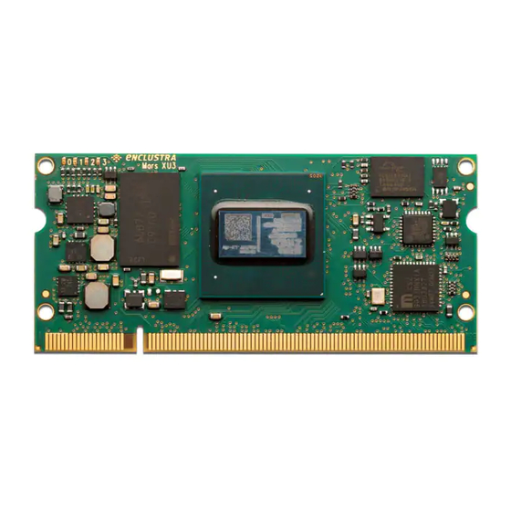
Page 13: Top And Bottom Views
Top and Bottom Views 2.4.1 Top View Figure 4: Module Top View 2.4.2 Bottom View Figure 5: Module Bottom View Please note that depending on the hardware revision and configuration, the module may look slightly dif- ferent than shown in this document. D-0000-432-001 13 / 52 Version 04, 25.07.2019... -
Page 14: Top And Bottom Assembly Drawings
Top and Bottom Assembly Drawings 2.5.1 Top Assembly Drawing Figure 6: Module Top Assembly Drawing 2.5.2 Bottom Assembly Drawing Figure 7: Module Bottom Assembly Drawing Please note that depending on the hardware revision and configuration, the module may look slightly dif- ferent than shown in this document. -
Page 15: Module Footprint
Module Connector The Mars XU3 SoC module fits into a 200-pin DDR2 SO-DIMM (1.8 V) socket. Up to four M2 screws may be used to mechanically fasten the module to the base board. Do not use excessive force to tighten the screws, as this could damage the module. -
Page 16: User I/O
User I/O 2.9.1 Pinout Information on the Mars XU3 SoC module pinout can be found in the Enclustra Mars Master Pinout [11], and in the additional document Enclustra Module Pin Connection Guidelines [10]. Warning! Please note that the pin types on the schematics symbol of the module connector and in the Master Pinout document are for reference only. -
Page 17: I/O Pin Exceptions
The information regarding the length of the signal lines from the MPSoC device to the module connector is available in Mars XU3 SoC Module IO Net Length Excel Sheet [3]. This enables the user to match the total length of the differential pairs on the base board if required by the application. -
Page 18: Vcc_Io Usage
VCC_IO_B[x], respectively VCC_CFG_[x] pins. All VCC_IO_B[x] or VCC_CFG_[x] pins of the same bank must be connected to the same voltage. For compatibility with other Enclustra Mars base boards and modules, it is recommended to use a single I/O voltage. -
Page 19: Signal Terminations
GPIOs; the suggested functions below are for reference only - always verify your MIO pinout with the Xilinx device handbook. Table 9 gives an overview over the MIO pin connections on the Mars XU3 SoC module. Only the pins marked with “user functionality” are available on the module connector. -
Page 20: Analog Inputs
MIO Group Function Connection QSPI flash QSPI flash QSPI feedback clock LEDs 0-2 On-board LEDs 10-11 On-board I2C bus and module connec- tor via level shifter I2C interrupt On-board I2C bus 13-22 eMMC flash eMMC flash LED3 On-board LEDs Enable signal for the 100 MHz oscillator On-board GTR 100 MHz oscillator Enable signal for the 27 MHz oscillator On-board GTR 27 MHz oscillator... -
Page 21: Multi-Gigabit Transceiver (Mgt)
Multi-Gigabit Transceiver (MGT) GTR Transceivers There are four GTR MGT pairs and two reference input clock differential pairs on the Mars XU3 SoC module connected to I/O bank 505, available on the module connector. The naming convention for the GTR MGT I/Os is: MGTPS_<FUNCTION>_<PACKAGE_PIN>_<POLARITY>. -
Page 22: Power
Power Generation Overview The Mars XU3 SoC module uses a 3.3 - 5.0 V DC power input for generating the on-board supply voltages (0.72/0.85/0.9 V, 0.85/0.9 V, 1.2 V, 1.8 V, 2.5 V). Some of these internally-generated voltages are accessible on the module connector. -
Page 23: Power Enable/Power Good
MIO pin 31) low. In this case the generated voltage for the PL core will be 0.72 V. The 0.9 V core supply for PS and PL is not supported, as the MPSoC devices equipped on the Mars XU3 SoC module are currently not available in speedgrade -3E, which would require a core voltage of 0.9 V. -
Page 24: Voltage Supply Outputs
For Enclustra Mars modules an Enclustra heat sink is available for purchase along with the product. It repre- sents an optimal solution to cool the Mars XU3 SoC module- it is low profile (less than 7 mm tall) and covers the whole module surface. -
Page 25: Voltage Monitoring
For details, please refer to the Enclustra website. Table 15 lists the heat sink and thermal pad part numbers that are compatible with the Mars XU3 SoC mod- ule. Details on these parts and additional information that may assist in selecting a suitable heat sink for the Mars XU3 SoC module can be found in the Enclustra Modules Heat Sink Application Note [18]. -
Page 26: Reset
A 24 MHz clock and a 25 MHz clock are used for the USB PHY and Ethernet PHY respectively. The crystal pads for the MPSoC RTC are connected to a 32.768 kHz oscillator on the Mars XU3 SoC module. Table 17 describes the clock connections to the MPSoC device. -
Page 27: Leds
LEDs There are four active-low user LEDs on the Mars XU3 SoC module - two of them are connected to both PS and PL and two of them are connected to PS only. On revision 1 modules, all LEDs are connected to both PL and PS. -
Page 28: Signal Description
In custom configurations up to 4 GB of SDRAM memory may be equipped on the module. 2.15.2 Signal Description Please refer to the Mars XU3 SoC Module FPGA Pinout Excel Sheet [4] for detailed information on the DDR4 SDRAM connections. 2.15.3... -
Page 29: Qspi Flash
Table 22 describes the memory availability and configuration on the Mars XU3 SoC module. As there is one QSPI flash chip equipped on the Mars XU3 SoC module, type “single” must be selected when programming the flash from Vivado tools. -
Page 30: Signal Description
512 Mbit Cypress (Spansion) Table 22: QSPI Flash Type Warning! Other flash memory devices devices may be equipped in future revisions of the Mars XU3 SoC module. Please check the user manual regularly for updates. 2.16.2 Signal Description The QSPI flash is connected to the PS MIO pins 0-5. Some of these signals are available on the module connector, allowing the user to program the QSPI flash from an external source. -
Page 31: Emmc Flash
VCC_CFG_MIO must be set to 1.8 V. Please note that this boot mode has not been tested, but it may be supported in the future. 2.19 Gigabit Ethernet A 10/100/1000 Mbit Ethernet PHY is available on the Mars XU3 SoC module, connected to the PS via RGMII interface. 2.19.1 Ethernet PHY Type Table 24 describes the equipped Ethernet PHY device type on the Mars XU3 SoC module. -
Page 32: Signal Description
2.19.3 External Connectivity The Ethernet signal lines can be connected directly to the magnetics. Please refer to the Enclustra Module Pin Connection Guidelines [10] for details regarding the connection of Ethernet signals. 2.19.4 MDIO Address The MDIO address assigned to the Gigabit Ethernet PHY is 3. -
Page 33: Usb 2.0
USB 2.0 The Mars XU3 SoC module has an on-board USB 2.0 PHY connected to the MPSoC device, to the PS to I/O bank 502. The USB interface can be configured for USB host, USB device and USB On-The-Go (host and device capable) operations. -
Page 34: Display Port
(PMU) - more information on the PMU is available in the Zynq UltraScale+ MPSoC Technical Reference Manual [19]. The RTC crystal pad input and crystal pad output are connected on the Mars XU3 SoC module to a 32.768 kHz oscillator. -
Page 35: Secure Eeprom
Manufacturer ATSHA204A-MAHDA-T (default) Atmel DS28CN01 (assembly option) Maxim Table 28: EEPROM Type An example demonstrating how to read data from the EEPROM is included in the Mars XU3 SoC module reference design [2]. D-0000-432-001 35 / 52 Version 04, 25.07.2019... -
Page 36: Device Configuration
3 Device Configuration Configuration Signals The PS of the MPSoC needs to be configured before the FPGA logic can be used. Xilinx Zynq devices need special boot images to boot from QSPI flash, eMMC flash or SD card. For more information, please refer to the Zynq UltraScale+ MPSoC Technical Reference Manual [19]. -
Page 37: Pull-Up During Configuration
All configuration signals except for BOOT_MODE must be high impedance as soon as the device is released from reset. Violating this rule may damage the equipped MPSoC device, as well as other devices on the Mars XU3 SoC module. Pull-Up During Configuration The Pull-Up During Configuration signal (PUDC) is pulled to GND on the module;... -
Page 38: Power-On Reset Delay Override
Figure 12: Pull-Up During Configuration (PUDC) Resistors - Assembly Drawing Bottom View (upper middle part) For details on the PUDC signal please refer to the Zynq UltraScale+ MPSoC Technical Reference Manual [19]. Power-on Reset Delay Override The power-on reset delay override MPSoC signal (POR_OVERRIDE) is pulled to GND on the module, setting the PL power-on delay time to the default standard time. -
Page 39: Boot Mode
For details on the POR_OVERRIDE signal please refer to the Zynq UltraScale+ MPSoC Technical Reference Manual [19]. Boot Mode The boot mode can be selected via two signals available on the module connector. Table 30 describes the available boot modes on the Mars XU3 SoC module. BOOT BOOT Mode... -
Page 40: Jtag On Module Connector
In the SD card boot mode the PS boots from the SD card located on the base board. There are two SD card boot modes available on the Mars XU3 SoC module. Please note that the SD boot mode with level shifter is currently not supported. -
Page 41: Emmc Flash Programming
Certain Xilinx tools versions support QSPI flash programming via JTAG only when JTAG boot mode is used (unavailable on the Mars XU3 SoC module). For more information, please refer to the Xilinx documentation [19] and support. Alternatively, the QSPI flash can be programmed in u-boot or Linux by the SPI controller in the PS or from an SPI external master. -
Page 42: Enclustra Module Configuration Tool
3.12 Enclustra Module Configuration Tool In combination with an Enclustra base board, the QSPI flash can be programmed using Enclustra Module Configuration Tool (MCT) [17]. For this method, a non-QSPI boot mode must be used during QSPI flash programming. The entire procedure is described in the reference design documentation, and is only avail- able starting with revision 2 modules. -
Page 43: I2C Communication
4 I2C Communication Overview The I2C bus on the Mars XU3 SoC module is connected to the MPSoC device and to the EEPROM, and is available on the module connector. This allows external devices to read the module type and to connect more devices to the I2C bus. -
Page 44: Secure Eeprom
An example demonstrating how to read the module information from the EEPROM memory is included in the Mars XU3 SoC module reference design. Warning! The secure EEPROM is for Enclustra use only. Any attempt to write data to the secure EEPROM causes the warranty to be rendered void. 4.4.1... -
Page 45: Product Information
Module Product Family Reserved Revision Product Information Mars XU3 SoC module 0x0330 0x[XX] 0x[YY] 0x0323 [XX][YY] Table 36: Product Information Module Configuration Addr. Bits Comment Min. Value Max. Value Comment MPSoC type See MPSoC type table (Table 38) 0x08 MPSoC device speed grade... -
Page 46: Mpsoc Speed Grades
Value MPSoC Speed Grade Table 39: MPSoC Speed Grades Table 40 shows the available temperature ranges. Value Module Temperature Range Commercial Extended Industrial Table 40: Module Temperature Range Ethernet MAC Address The Ethernet MAC address is stored using big-endian byte order (MSB on the lowest address). Each module is assigned two sequential MAC addresses;... -
Page 47: Operating Conditions
5 Operating Conditions Absolute Maximum Ratings Table 41 indicates the absolute maximum ratings for Mars XU3 SoC module. The values given are for ref- erence only; for details please refer to the Zynq UltraScale+ MPSoC, DC and AC Switching Characteristics Datasheet [21]. -
Page 48: Recommended Operating Conditions
Recommended Operating Conditions Table 42 indicates the recommended operating conditions for Mars XU3 SoC module. The values given are for reference only; for details please refer to the Zynq UltraScale+ MPSoC, DC and AC Switching Character- istics Datasheet [21]. Symbol... -
Page 49: Ordering And Support
6 Ordering and Support Ordering Please use the Enclustra online request/order form for ordering or requesting information: http://www.enclustra.com/en/order/ Support Please follow the instructions on the Enclustra online support site: http://www.enclustra.com/en/support/ D-0000-432-001 49 / 52 Version 04, 25.07.2019... - Page 50 List of Figures Hardware Block Diagram ........10 Product Code Fields .
- Page 51 EEPROM Sector 0 Memory Map ........44 Product Information .
- Page 52 [1] Enclustra General Business Conditions http://www.enclustra.com/en/products/gbc/ [2] Mars XU3 SoC Module Reference Design Ask Enclustra for details [3] Mars XU3 SoC Module IO Net Length Excel Sheet Ask Enclustra for details [4] Mars XU3 SoC Module FPGA Pinout Excel Sheet Ask Enclustra for details...
Need help?
Do you have a question about the Mars XU3 and is the answer not in the manual?
Questions and answers