Table of Contents
Advertisement
Quick Links
Mars AX3 FPGA Module
Purpose
The purpose of this document is to present the characteristics of Mars AX3 FPGA module to the user, and
to provide the user with a comprehensive guide to understanding and using the Mars AX3 FPGA module.
Summary
This document first gives an overview of the Mars AX3 FPGA module followed by a detailed description of
its features and configuration options. In addition, references to other useful documents are included.
Product Information
Product
Document Information
Reference / Version / Date
Approval Information
Written by
Verified by
Approved by
User Manual
Code
MA-AX3
Reference
D-0000-426-004
Name
DIUN
GLAC
DIUN
Enclustra GmbH – Räffelstrasse 28 – CH-8045 Zürich – Switzerland
Name
Mars AX3 FPGA Module
Version
06
Position
Design Engineer
Design Expert
Manager, BU SP
Phone +41 43 343 39 43 – www.enclustra.com
Date
16.02.2021
Date
05.08.2016
29.08.2016
16.02.2021
Advertisement
Chapters
Table of Contents

Related Manuals for Enclustra Mars AX3


Summary of Contents for Enclustra Mars AX3
- Page 1 User Manual Purpose The purpose of this document is to present the characteristics of Mars AX3 FPGA module to the user, and to provide the user with a comprehensive guide to understanding and using the Mars AX3 FPGA module. Summary This document first gives an overview of the Mars AX3 FPGA module followed by a detailed description of its features and configuration options.
- Page 2 Unauthorized duplication of this document, in whole or in part, by any means is prohibited without the prior written permission of Enclustra GmbH, Switzerland. Although Enclustra GmbH believes that the information included in this publication is correct as of the date of publication, Enclustra GmbH reserves the right to make changes at any time without notice.
-
Page 3: Table Of Contents
Enclustra Heat Sink ........ - Page 4 Signal Description ..........36 Enclustra Module Configuration Tool ........37 I2C Communication Overview .
-
Page 5: Overview
Please note that the warranty of an Enclustra module is voided if the FPGA fuses are blown. This operation is done at own risk, as it is irreversible. Enclustra cannot test the module in case of a warranty product return. -
Page 6: Electrostatic Discharge
1.1.7 Electromagnetic Compatibility The Mars AX3 FPGA module is a Class A product (as defined in IEC 61000-3-2 standard) and is not in- tended for use in domestic environments. The product may cause electromagnetic interference, for which appropriate measures must be taken. -
Page 7: Accessories
The reference design can be downloaded from Github: https://github.com/enclustra. 1.4.2 Enclustra Heat Sink For Mars modules an Enclustra heat sink is available for purchase along with the product. Please refer to section 2.10.6 for further information on the available cooling options. 1.4.3... -
Page 8: Mars St3 Base Board
Please note that the available features depend on the equipped Mars module type. Xilinx Tool Support The FPGA devices equipped on the Mars AX3 FPGA module are supported by the Vivado HL WebPACK Edition software, which is available free of charge. Please contact Xilinx for further information. -
Page 9: Module Description
Figure 1: Hardware Block Diagram The main component of the Mars AX3 FPGA module is the Xilinx Artix-7 FPGA device. Most of its I/O pins are connected to the Mars module connector, making 108 user I/Os available to the user. With some hardware changes, four additional FPGA pins can be routed to the module connector, in case the application requires 112 user I/Os and a custom base board is used. -
Page 10: Article Numbers And Article Codes
The correspondence between article number and article code is shown in Table 2. The article code repre- sents the product code, followed by the revision; the R suffix and number represent the revision number. The revision changes and product known issues are described in the Mars AX3 FPGA Module Known Issues and Changes document [6]. -
Page 11: Article Numbers And Article Codes
Article Number Article Code EN100030 MA-AX3-100-2I-D8-R1 EN100081 MA-AX3-100-1C-D8-R1 EN100587 MA-AX3-100-1C-D8-R1 EN100655 MA-AX3-35-1I-D8-R2 EN100656 MA-AX3-50-1C-D8-R2 EN100657 MA-AX3-50-1I-D8-R2 EN100722 MA-AX3-100-1C-D8-R2 EN100723 MA-AX3-100-2I-D8-R2 EN100908 MA-AX3-35-1C-D8-R2 EN100909 MA-AX3-50-1C-D8-R2 EN101294 MA-AX3-35-1C-D8-R3 EN101295 MA-AX3-35-1I-D8-R3 EN101296 MA-AX3-50-1C-D8-R3 EN101297 MA-AX3-50-1I-D8-R3 EN101298 MA-AX3-100-1C-D8-R3 EN101299 MA-AX3-100-2I-D8-R3 Table 2: Article Numbers and Article Codes D-0000-426-004 11 / 47 Version 06, 16.02.2021... -
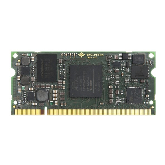
Page 12: Top And Bottom Views
Top and Bottom Views 2.4.1 Top View Figure 4: Module Top View 2.4.2 Bottom View Figure 5: Module Bottom View Please note that depending on the hardware revision and configuration, the module may look slightly dif- ferent than shown in this document. D-0000-426-004 12 / 47 Version 06, 16.02.2021... -
Page 13: Top And Bottom Assembly Drawings
Top and Bottom Assembly Drawings 2.5.1 Top Assembly Drawing Figure 6: Module Top Assembly Drawing 2.5.2 Bottom Assembly Drawing Figure 7: Module Bottom Assembly Drawing Please note that depending on the hardware revision and configuration, the module may look slightly dif- ferent than shown in this document. -
Page 14: Module Footprint
Module Connector The Mars AX3 FPGA module fits into a 200-pin DDR2 SO-DIMM (1.8 V) socket. Up to four M2 screws may be used to mechanically fasten the module to the base board. Do not use excessive force to tighten the screws, as this could damage the module. -
Page 15: User I/O
User I/O 2.9.1 Pinout Information on the Mars AX3 FPGA module pinout can be found in the Enclustra Mars Master Pinout [11], and in the additional document Enclustra Module Pin Connection Guidelines [10]. Warning! Please note that the pin types on the schematics symbol of the module connector and in the Master Pinout document are for reference only. -
Page 16: Differential I/Os
The information regarding the length of the signal lines from the FPGA device to the module connector is available in Mars AX3 FPGA Module IO Net Length Excel Sheet [3]. This enables the user to match the total length of the differential pairs on the base board if required by the application. -
Page 17: Vref Usage
FPGA device, as well as other devices on the Mars AX3 FPGA module. Do not leave a VREF pin floating when the used I/O standard requires a reference voltage, as this may damage the equipped FPGA device, as well as other devices on the Mars AX3 FPGA module. 2.9.5... -
Page 18: Signal Terminations
Internal differential termination is available only for certain VCCO voltages; please refer to Xilinx AR# 43989 for details. Single-Ended Outputs There are no series termination resistors on the Mars AX3 FPGA module for single-ended outputs. If required, series termination resistors may be equipped on the base board (close to the module pins). 2.9.7 Analog Inputs The Artix-7 FPGA devices provide a dual 12-bit ADC. -
Page 19: Power
Power Generation Overview The Mars AX3 FPGA module uses a 3.3 - 5.0 V DC power input for generating the on-board supply voltages (1.0 V, 1.35 V/1.5 V, 1.8 V). These internally-generated voltages are accessible on the module connector. In addition, a separate 3.3 V power input is used to supply peripherals, such as the Ethernet PHY, QSPI flash,... -
Page 20: Power Enable/Power Good
DC/DC converters for 1.0 V, 1.35 V/1.5 V and 1.8 V, leaving the FPGA device and the DDR3 SDRAM unpowered. The PWR_EN input is pulled to VCC_3V3 on the Mars AX3 FPGA module with a 10 k resistor. The PWR_GOOD signal is pulled to VCC_3V3 on the Mars AX3 FPGA module with a 10 k resistor. -
Page 21: Voltage Supply Outputs
Battery voltage for the RTC and FPGA en- cryption key storage Table 11: Voltage Supply Inputs 2.10.4 Voltage Supply Outputs Table 12 presents the supply voltages generated on the Mars AX3 FPGA module, that are available on the module connector. Pin Name Module Connector Pins Voltage... -
Page 22: Heat Dissipation
For Mars modules an Enclustra heat sink is available for purchase along with the product. It represents an optimal solution to cool the Mars AX3 FPGA module - it is low profile (less than 7 mm tall) and covers the whole module surface. -
Page 23: Clock Generation
Clock Generation A 50 MHz oscillator is used for the Mars AX3 FPGA module clock generation; the 50 MHz clock is fed to the FPGA logic. The 25 MHz clock for the Ethernet PHYs is generated from the 50 MHz system oscillator. Table 15 describes the clock connections. -
Page 24: Ddr3 Sdram
2.14 DDR3 SDRAM The DDR3 SDRAM on the Mars AX3 FPGA module is operated at 1.35 V (low power mode) or at 1.5 V, de- pending on a selection signal. The DDR bus width is 16-bit. The maximum memory bandwidth on the Mars AX3 FPGA module is:... -
Page 25: Termination
2.14.4 Parameters Please refer to the Mars AX3 FPGA module reference design [2] for DDR3 settings guidelines. The DDR3 SDRAM parameters to be set in Vivado project are presented in Table 19. If the memory part equipped on the module is not available in Vivado, a custom memory part can be created and configured as described in the table. -
Page 26: Qspi Flash
Table 20: QSPI Flash Types Warning! Other flash memory devices may be equipped in future revisions of the Mars AX3 FPGA module. Please check the user manual regularly for updates. Any parts with different speeds and temperature ranges that fulfill the requirements for the module variant may be used. -
Page 27: Gigabit Ethernet
FPGA and the flash device. 2.16 Gigabit Ethernet A 10/100/1000 Mbit Ethernet PHY is available on the Mars AX3 FPGA module, connected to the FPGA via RGMII interface. 2.16.1 Ethernet PHY Type Table 22 describes the equipped Ethernet PHY device type on the Mars AX3 FPGA module. -
Page 28: Real-Time Clock (Rtc)
RTC on Revision 2 On the Mars AX3 FPGA module revision 2 the interrupt line from the RTC is not active by default. In order to perform this connection, resistor R600 must be assembled; please contact Enclustra support for details. -
Page 29: Secure Eeprom
An example demonstrating how to use the RTC is included in the Mars AX3 FPGA module reference design [2], in the I2C example program. Note that the software does not perform automatically the reading of the RTC, as this circuit is not equipped in the standard configuration; however, the code can be easily modified to call the function that reads the values from the real-time clock. -
Page 30: Device Configuration
3 Device Configuration Configuration Signals Table 26 describes the most important configuration pins. Some of the pins are connected to a user I/O, as well as to a special purpose configuration pin. This is done for compatibility with other Mars modules, on which the configuration pins can be used as user I/Os after configuration. -
Page 31: Configuration Mode
All configuration signals except for FPGA_MODE must be high impedance as soon as the device is released from reset. Violating this rule may damage the equipped FPGA device, as well as other devices on the Mars AX3 FPGA module. Configuration Mode The FPGA_MODE signals determine whether the FPGA device is configured from the QSPI flash or serially via SPI from an external device. -
Page 32: Pull-Up During Configuration (Pudc)
Figure 10 illustrates the configuration of the I/O signals during power-up. Figure 11 indicates the location of the pull-up/pull-down resistors on the module PCB - upper right part on the top view drawing. Figure 10: Pull-Up During Configuration (PUDC) D-0000-426-004 32 / 47 Version 06, 16.02.2021... -
Page 33: Jtag
The Winbond flash equipped on revisions 1 and 2 is not supported by Vivado (and only partially supported in iMPACT); please use Enclustra MCT [15] to program the QSPI flash. Section 3.7 gives a detailed description on the QSPI flash configuration options via JTAG. -
Page 34: Master Serial Configuration
Master Serial Configuration In the master serial configuration mode, the FPGA reads the bitstream from the QSPI flash. The configuration clock can be configured up to 26 MHz and quad-SPI booting is supported. Higher configuration clocks can be achieved by using the advanced configuration settings of the Xilinx tools. For more information on the configuration modes, please refer to the 7 Series FPGAs Configuration User Guide [18]. -
Page 35: Signal Description
Xilinx AR #42128. QSPI Flash Programming via JTAG Enclustra MCT [15] can be used to program the QSPI flash equipped on any Mars AX3 FPGA module revision as an alternative to programming via JTAG. -
Page 36: Qspi Flash Programming From An External Spi Master
Figure 12: QSPI Flash Programming from an External SPI Master - Signal Diagrams Warning! Accessing the QSPI flash directly without putting the FPGA device into reset may damage the equipped FPGA device, as well as other devices on the Mars AX3 FPGA module. 3.8.1 Signal Description... -
Page 37: Enclustra Module Configuration Tool
Enclustra Module Configuration Tool In combination with an Enclustra base board, the QSPI flash can be programmed using the Enclustra Mod- ule Configuration Tool (MCT) [15]. Slave serial configuration is also supported by the Enclustra MCT software. D-0000-426-004 37 / 47... -
Page 38: I2C Communication
4 I2C Communication Overview The I2C bus on the Mars AX3 FPGA module is connected to the FPGA device, EEPROM and RTC, and is available on the module connector. This allows external devices to read the module type and to connect more devices to the I2C bus. -
Page 39: Secure Eeprom
An example demonstrating how to read the module information from the EEPROM memory is included in the Mars AX3 FPGA module reference design. Warning! The secure EEPROM is for Enclustra use only. Any attempt to write data to the secure EEPROM causes the warranty to be rendered void. 4.4.1... -
Page 40: Product Information
(MSB on the lowest address). Module Product Information This field indicates the type of module and hardware revision. Module Product Family Reserved Revision Product Information Mars AX3 FPGA module 0x0324 0x[XX] 0x[YY] 0x0324 [XX][YY] Table 35: Product Information Module Configuration Addr. -
Page 41: Fpga Device Types
Value FPGA Device Type Not used XC7A35T XC7A50T XC7A75T XC7A100T Table 37: FPGA Device Types Ethernet MAC Address The Ethernet MAC address is stored using big-endian byte order (MSB on the lowest address). Each module is assigned two sequential MAC addresses; only the lower one is stored in the EEPROM. D-0000-426-004 41 / 47 Version 06, 16.02.2021... -
Page 42: Operating Conditions
5 Operating Conditions Absolute Maximum Ratings Table 38 indicates the absolute maximum ratings for Mars AX3 FPGA module. The values given are for reference only; for details please refer to the Artix-7 Datasheet [19]. Symbol Description Rating Unit VCC_MOD Supply voltage relative to GND -0.5 to 6... -
Page 43: Recommended Operating Conditions
Recommended Operating Conditions Table 39 indicates the recommended operating conditions for Mars AX3 FPGA module. The values given are for reference only; for details please refer to the Artix-7 Datasheet [19]. Symbol Description Rating Unit VCC_MOD Supply voltage relative to GND 3.0 to 5.5... -
Page 44: Ordering And Support
6 Ordering and Support Ordering Please use the Enclustra online request/order form for ordering or requesting information: http://www.enclustra.com/en/order/ Support Please follow the instructions on the Enclustra online support site: http://www.enclustra.com/en/support/ D-0000-426-004 44 / 47 Version 06, 16.02.2021... - Page 45 List of Figures Hardware Block Diagram ........Product Code Fields .
- Page 46 Recommended Operating Conditions ....... . . 43 D-0000-426-004 46 / 47 Version 06, 16.02.2021...
- Page 47 [1] Enclustra General Business Conditions http://www.enclustra.com/en/products/gbc/ [2] Mars AX3 FPGA Module Reference Design https://github.com/enclustra [3] Mars AX3 FPGA Module IO Net Length Excel Sheet Ask Enclustra for details [4] Mars AX3 FPGA Module FPGA Pinout Excel Sheet Ask Enclustra for details...
Need help?
Do you have a question about the Mars AX3 and is the answer not in the manual?
Questions and answers