Table of Contents
Advertisement
Quick Links
Mercury+ XU7 SoC Module
Purpose
The purpose of this document is to present the characteristics of Mercury+ XU7 SoC module to the user,
and to provide the user with a comprehensive guide to understanding and using the Mercury+ XU7 SoC
module.
Summary
This document first gives an overview of the Mercury+ XU7 SoC module followed by a detailed description
of its features and configuration options. In addition, references to other useful documents are included.
Product Information
Product
Document Information
Reference / Version / Date
Approval Information
Written by
Verified by
Approved by
User Manual
Code
ME-XU7
Reference
D-0000-443-001
Name
DIUN, MMOS
GKOE, RPAU
DIUN
Enclustra GmbH – Räffelstrasse 28 – CH-8045 Zürich – Switzerland
Name
Mercury+ XU7 SoC Module
Version
06
Position
Design Engineer
Design Expert
Manager, BU SP
Phone +41 43 343 39 43 – www.enclustra.com
Date
18.11.2019
Date
03.09.2018
10.09.2018
18.11.2019
Advertisement
Table of Contents

Related Manuals for Enclustra Mercury+ XU7


Summary of Contents for Enclustra Mercury+ XU7
- Page 1 Mercury+ XU7 SoC Module User Manual Purpose The purpose of this document is to present the characteristics of Mercury+ XU7 SoC module to the user, and to provide the user with a comprehensive guide to understanding and using the Mercury+ XU7 SoC module.
- Page 2 Unauthorized duplication of this document, in whole or in part, by any means is prohibited without the prior written permission of Enclustra GmbH, Switzerland. Although Enclustra GmbH believes that the information included in this publication is correct as of the date of publication, Enclustra GmbH reserves the right to make changes at any time without notice.
-
Page 3: Table Of Contents
Enclustra Build Environment ........ - Page 4 3.13 Enclustra Module Configuration Tool ........49 I2C Communication Overview .
- Page 5 Operating Conditions Absolute Maximum Ratings ........54 Recommended Operating Conditions .
-
Page 6: Overview
The Enclustra Build Environment [14] is available for the Mercury+ XU7 SoC module. This build system allows the user to quickly set up and run Linux on any Enclustra SoC module. It allows the user to choose the desired target and download all the required binaries, such as bitstream and FSBL (First Stage Boot Loader). -
Page 7: Electrostatic Discharge
Warning! It is possible to mount the Mercury+ XU7 SoC module the wrong way round on the base board - always check that the mounting holes on the base board are aligned with the mounting holes of the Mercury+ XU7 SoC module. -
Page 8: Deliverables
Enclustra Build Environment The Enclustra Build Environment (EBE) [14] enables the user to quickly set up and run Linux on any Enclustra SoC module or system board. It allows the user to choose the desired target, and download all the required binaries, such as bitstream and FSBL. -
Page 9: Mercury+ Pe1 Base Board
FMC interfaces, the compatibility of the Mercury+ XU7 SoC module to the Mercury+ PE1 base board is limited. It is recommended to check the FMC card pinout in detail with the Enclustra Mercury Master Pinout and with the module and base board schematics. -
Page 10: Module Description
Block Diagram Figure 1: Hardware Block Diagram The main component of the Mercury+ XU7 SoC module is the Xilinx Zynq Ultrascale+ MPSoC device. Most of its I/O pins are connected to the Mercury+ module connector, making 136 regular user I/Os available to the user. -
Page 11: Module Configuration And Product Codes
Figure 2: Product Code Fields Please note that for the first revision modules or early access modules, the product code may not respect entirely this naming convention. Please contact Enclustra for details on this aspect. Article Numbers and Article Codes Every module is uniquely labeled, showing the article number and serial number. -
Page 12: Module Label
The correspondence between article number and article code is shown in Table 2. The article code repre- sents the product code, followed by the revision; the R suffix and number represent the revision number. The revision changes and product known issues are described in the Mercury+ XU7 SoC Module Known Issues and Changes document [6]. -
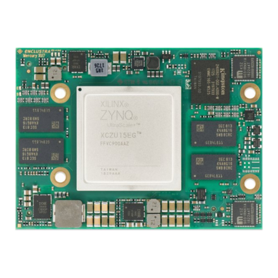
Page 13: Top And Bottom Views
Top and Bottom Views 2.4.1 Top View Figure 4: Module Top View 2.4.2 Bottom View Figure 5: Module Bottom View Please note that depending on the hardware revision and configuration, the module may look slightly dif- ferent than shown in this document. D-0000-443-001 13 / 59 Version 06, 18.11.2019... -
Page 14: Top And Bottom Assembly Drawings
Top and Bottom Assembly Drawings 2.5.1 Top Assembly Drawing Figure 6: Module Top Assembly Drawing 2.5.2 Bottom Assembly Drawing Figure 7: Module Bottom Assembly Drawing Please note that depending on the hardware revision and configuration, the module may look slightly dif- ferent than shown in this document. -
Page 15: Module Footprint
Figure 8: Module Footprint - Top View Warning! It is possible to mount the Mercury+ XU7 SoC module the wrong way round on the base board - always check that the mounting holes on the base board are aligned with the mounting holes of the Mercury+ XU7 SoC module. -
Page 16: Module Connector
Symbol Value Size 54 mm Component height top 3.42 mm Component height bottom 1.35 mm Weight 38 g Table 3: Mechanical Data Module Connector Three Hirose FX10 168-pin 0.5 mm pitch headers with a total of 504 pins have to be integrated on the base board. -
Page 17: User I/O
User I/O 2.9.1 Pinout Information on the Mercury+ XU7 SoC module pinout can be found in the Enclustra Mercury Master Pinout [11], and in the additional document Enclustra Module Pin Connection Guidelines [10]. Warning! Please note that the pin types on the schematics symbol of the module connector and in the Master Pinout document are for reference only. -
Page 18: I/O Pin Exceptions
The I/O pin exceptions are pins with special functions or restrictions (for example, when used in combination with certain Mercury boards they may have a specific role). PCIe Reset Signal (PERST#) Table 6 lists the I/O pin exceptions on the Mercury+ XU7 SoC module related to the PCIe reset connection. I/O Name Module Connector Pin... -
Page 19: Differential I/Os
MIO30/42 does not apply in this case). I/O Pins with Level Shifter There are four signals on the Mercury+ XU7 SoC module that are routed from the FPGA banks to the module connector via level shifters - these are presented in Table 7. -
Page 20: Vcc_Io Usage
VCC_IO_B[x], respectively VCC_CFG_[x] pins. All VCC_IO_B[x] or VCC_CFG_[x] pins of the same bank must be connected to the same voltage. For compatibility with other Enclustra Mercury modules, it is recommended to use a single I/O voltage per module connector. - Page 21 C are used on other Enclustra modules; for compatibility purposes it is acceptable to power these pins even if they are not used on the Mercury+ XU7 SoC module. The Mercury+ XU7 SoC module may be used in combination with base boards having only two module connectors.
-
Page 22: Signal Terminations
GPIOs; the suggested functions below are for reference only - always verify your MIO pinout with the Xilinx device handbook. Table 10 gives an overview over the MIO pin connections on the Mercury+ XU7 SoC module. Only the pins marked with “user functionality” are available on the module connector. -
Page 23: Analog Inputs
MIO Group Function Connection QSPI flash QSPI flash QSPI feedback clock Unused 10-11 On-board I2C bus and module connector via level shifter I2C interrupt On-board I2C bus 13-22 eMMC flash eMMC flash USB PHY 1 reset USB 2.0 PHY 1 24-25 LED0#, LED1# On-board LEDs... -
Page 24: Multi-Gigabit Transceiver (Mgt)
(connected to the PL) and GTR transceivers (connected to the PS). GTH Transceivers There are 16 GTH MGTs available on the Mercury+ XU7 SoC module organized in four FPGA banks - Table 12 describes the connections. The naming convention for the GTH MGT I/Os is: MGT_B<BANK>_<FUNCTION>_<PACKAGE_PIN>_<POLARITY>. -
Page 25: Mgt Pairs
GTR Transceivers There are four GTR MGT pairs and two reference input clock differential pairs on the Mercury+ XU7 SoC module connected to I/O bank 505; these are routed to module connector B. The naming convention for the GTR MGT I/Os is: MGTPS_<FUNCTION>_<PACKAGE_PIN>_<POLARITY>. -
Page 26: Power
Power Generation Overview The Mercury+ XU7 SoC module uses a 5 - 15 V DC power input for generating the on-board supply voltages (0.72/0.85/0.9 V, 0.85/0.9 V, 0.9 V, 1.2 V, 1.8 V, 2.5 V, 3.3 V and 5.0 V). Some of these voltages (1.8 V, 2.5 V, 3.3 V) are accessible on the module connector. -
Page 27: Power Enable/Power Good
Power Enable/Power Good The Mercury+ XU7 SoC module provides a power enable input on the module connector. This input may be used to shut down the DC/DC converters and LDOs for 0.72/0.85/0.9 V, 0.85/0.9 V, 0.9 V, 1.2 V, 1.8 V and 2.5 V. -
Page 28: Voltage Supply Inputs
In this case, VCC_IO needs to be switched off in the manner indicated in Figure 10. 2.11.3 Voltage Supply Inputs Table 16 describes the power supply inputs on the Mercury+ XU7 SoC module. The VCC voltages used as supplies for the I/O banks are described in Section 2.9.5. Pin Name Module Connector Pins... -
Page 29: Power Consumption
MPSoC is adequately cooled. Table 18 lists the heat sink and thermal pad part numbers that are compatible with the Mercury+ XU7 SoC module. Details on these parts and additional information that may assist in selecting a suitable heat sink for the Mercury+ XU7 SoC module can be found in the Enclustra Modules Heat Sink Application Note [17]. -
Page 30: Voltage Monitoring
2.11.7 Voltage Monitoring Several pins on the module connector on the Mercury+ XU7 SoC module are marked as VMON. These are voltage monitoring outputs that may be used to measure some of the on-board voltages. Examples of such monitoring circuits are available on Enclustra base boards. -
Page 31: Reset
Please note that PS_POR# is automatically asserted if PWR_GOOD is low. 2.14 LEDs There are three active-low user LEDs on the Mercury+ XU7 SoC module - two of them are connected to the PS and one connected to the PL. D-0000-443-001 31 / 59 Version 06, 18.11.2019... -
Page 32: Ddr4 Sdram (Ps)
DDR4 SDRAM (PS) There are two DDR4 SDRAM channels on the Mercury+ XU7 SoC module: one attached directly to the PS side (which is available only as a shared resource to the PL side) and one attached directly to the PL side. -
Page 33: Signal Description
Please check the user manual regularly for updates. Any parts with different speed bins or temperature ranges that fulfill the requirements for the module variant may be used. 2.15.2 Signal Description Please refer to the Mercury+ XU7 SoC Module FPGA Pinout Excel Sheet [4] for detailed information on the DDR4 SDRAM connections. 2.15.3 Termination Warning! No external termination is implemented for the data signals on the Mercury+ XU7 SoC module. -
Page 34: Ddr4 Sdram (Pl)
The DDR4 SDRAM memory controller on the MPSoC device supports speeds up to 2666 Mbit/s (1333 MHz), however the memories equipped on the Mercury+ XU7 SoC module are rated 2400 Mbit/s (1200 MHz). The maximum PL memory bandwidth on the Mercury+ XU7 SoC module is:... -
Page 35: Ddr4 Sdram Type
Please check the user manual regularly for updates. Any parts with different speed bins or temperature ranges that fulfill the requirements for the module variant may be used. 2.16.2 Signal Description Please refer to the Mercury+ XU7 SoC Module FPGA Pinout Excel Sheet [4] for detailed information on the DDR4 SDRAM connections. 2.16.3 Termination Warning! No external termination is implemented for the data signals on the Mercury+ XU7 SoC module. -
Page 36: Qspi Flash
Table 28 describes the memory availability and configuration on the Mercury+ XU7 SoC module. As there is one QSPI flash chip equipped on the Mercury+ XU7 SoC module, type “single” must be selected when programming the flash from Vivado tools. -
Page 37: Configuration
16 GB Kingston Table 29: eMMC Flash Type Warning! Other flash memory devices may be equipped in future revisions of the Mercury+ XU7 SoC module. Please check the user manual regularly for updates. D-0000-443-001 37 / 59 Version 06, 18.11.2019... -
Page 38: Signal Description
VCC_CFG_MIO must be set to 1.8 V. Please note that this boot mode has not been tested, but it may be supported in the future. 2.20 Dual Gigabit Ethernet Two 10/100/1000 Mbit Ethernet PHYs are available on the Mercury+ XU7 SoC module, both connected to the PS via RGMII interfaces 2.20.1 Ethernet PHY Type Table 30 describes the equipped Ethernet PHY devices type on the Mercury+ XU7 SoC module. -
Page 39: External Connectivity
Ethernet PHYs is connected to the I2C interrupt line, available on MIO pin 12. 2.20.3 External Connectivity The Ethernet signal lines can be connected directly to the magnetics. Please refer to the Enclustra Module Pin Connection Guidelines [10] for details regarding the connection of Ethernet signals. 2.20.4... -
Page 40: Rgmii Delays Configuration
USB 2.0 Two USB 2.0 PHYs are available on the Mercury+ XU7 SoC module, both connected to the PS to I/O bank 502. USB PHY 0 can be configured as host or device and USB PHY 1 can be used only as host. -
Page 41: Signal Description
PHY Type Manufacturer Type USB3320C Microchip USB 2.0 PHY Table 34: USB 2.0 PHY Type 2.21.2 Signal Description The ULPI interface for the PHY 0 is connected to MIO pins 52-63 for use with the integrated USB controller. The ULPI interface for the PHY 1 is connected to MIO pins 64-75. The MIO signals are shared between Ethernet PHY 1 and USB PHY 1, therefore only one of them can be used. -
Page 42: Display Port
(PMU) - more information on the PMU is available in the Zynq UltraScale+ MPSoC Technical Reference Manual [18]. The RTC crystal pad input and crystal pad output are connected on the Mercury+ XU7 SoC module to a 32.768 kHz oscillator. -
Page 43: Device Configuration
3 Device Configuration Configuration Signals The PS of the MPSoC needs to be configured before the FPGA logic can be used. Xilinx Zynq devices need special boot images to boot from QSPI flash, eMMC flash or SD card. For more information, please refer to the Zynq UltraScale+ MPSoC Technical Reference Manual [18]. -
Page 44: Module Connector C Detection
VCC_IO pins on connector C are not used, C_PRSNT# does not influence the behavior of the module. For compatibility with other Enclustra modules, it is recommended to connect C_PRSNT# to GND on the base board if the designed base board has three connectors. -
Page 45: Power-On Reset Delay Override
The boot mode can be selected via two signals available on the module connector. Table 37 describes the available boot modes on the Mercury+ XU7 SoC module. Starting with revision 2, JTAG boot mode has been introduced to increase the usability with Xilinx tools, which may report issues when programming the on-board QSPI flash or when loading the FPGA bitstream in a non-JTAG boot mode. -
Page 46: Jtag
Certain Xilinx tool versions support QSPI flash programming via JTAG only when JTAG boot mode is used (unavailable on the Mercury+ XU7 SoC module). Alternatively, the QSPI flash can be programmed in u-boot or Linux by the SPI controller in the PS or from an SPI external master. -
Page 47: External Connectivity
The VREF pin of the programmer must be connected to VCC_CFG_MIO. It is recommended to add 22 series termination resistors between the module and the JTAG header, close to the source. Please refer to the Enclustra Module Pin Connection Guidelines for details on JTAG interface. 3.6.3 JTAG Boot Mode Starting with revision 2, support for JTAG boot mode has been added to increase the usability of the module with Xilinx tools, for example for QSPI flash programming or FPGA bitstream loading. -
Page 48: Emmc Boot Mode
In the SD card boot mode the PS boots from the SD card located on the base board. There are two SD card boot modes available on the Mercury+ XU7 SoC module. Please note that the SD boot mode with level shifter is currently not supported. -
Page 49: Qspi Flash Programming From An External Spi Master
3.13 Enclustra Module Configuration Tool In combination with an Enclustra base board, the QSPI flash can be programmed using Enclustra Module Configuration Tool (MCT) [16]. For this method, a non-QSPI boot mode must be used during QSPI flash programming. The entire procedure is described in the reference design documentation. -
Page 50: I2C Communication
4 I2C Communication Overview The I2C bus on the Mercury+ XU7 SoC module is connected to the MPSoC device and to the EEPROM, and is available on the module and debug connectors. This allows external devices to read the module type and to connect more devices to the I2C bus. -
Page 51: Secure Eeprom
An example demonstrating how to read the module information from the EEPROM memory is included in the Mercury+ XU7 SoC module reference design. Warning! The secure EEPROM is for Enclustra use only. Any attempt to write data to the secure EEPROM causes the warranty to be rendered void. 4.4.1... -
Page 52: Product Information
Module Product Family Reserved Revision Product Information Mercury+ XU7 SoC module 0x0334 0x[XX] 0x[YY] 0x0334 [XX][YY] Table 43: Product Information Module Configuration Addr. Bits Comment Min. Value Max. Value Comment MPSoC type See MPSoC type table (Table 45) 0x08 MPSoC device speed grade... -
Page 53: Module Temperature Range
Value Module Temperature Range Commercial Extended Industrial Table 46: Module Temperature Range Ethernet MAC Address The Ethernet MAC address is stored using big-endian byte order (MSB on the lowest address). Each module is assigned two sequential MAC addresses; only the lower one is stored in the EEPROM. D-0000-443-001 53 / 59 Version 06, 18.11.2019... -
Page 54: Operating Conditions
5 Operating Conditions Absolute Maximum Ratings Table 47 indicates the absolute maximum ratings for Mercury+ XU7 SoC module. The values given are for reference only; for details please refer to the Zynq UltraScale+ MPSoC, DC and AC Switching Characteristics Datasheet [20]. -
Page 55: Recommended Operating Conditions
Recommended Operating Conditions Table 48 indicates the recommended operating conditions for Mercury+ XU7 SoC module. The values given are for reference only; for details please refer to the Zynq UltraScale+ MPSoC, DC and AC Switching Characteristics Datasheet [20]. Symbol Description... -
Page 56: Ordering And Support
6 Ordering and Support Ordering Please use the Enclustra online request/order form for ordering or requesting information: http://www.enclustra.com/en/order/ Support Please follow the instructions on the Enclustra online support site: http://www.enclustra.com/en/support/ D-0000-443-001 56 / 59 Version 06, 18.11.2019... - Page 57 List of Figures Hardware Block Diagram ........10 Product Code Fields .
- Page 58 MPSoC Configuration Pins ........43 Boot Modes .
- Page 59 [1] Enclustra General Business Conditions http://www.enclustra.com/en/products/gbc/ [2] Mercury+ XU7 SoC Module Reference Design Ask Enclustra for details [3] Mercury+ XU7 SoC Module IO Net Length Excel Sheet Ask Enclustra for details [4] Mercury+ XU7 SoC Module FPGA Pinout Excel Sheet Ask Enclustra for details...
Need help?
Do you have a question about the Mercury+ XU7 and is the answer not in the manual?
Questions and answers