Table of Contents
Advertisement
Quick Links
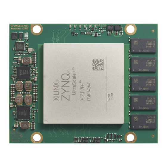
Andromeda XZU90 Module
Purpose
The purpose of this document is to present the characteristics of Andromeda XZU90 module to the user,
and to provide the user with a comprehensive guide to understanding and using the Andromeda XZU90
module.
Summary
This document first gives an overview of the Andromeda XZU90 module followed by a detailed descrip-
tion of its features and configuration options. In addition, references to other useful documents are
included.
Product Information
Product
Document Information
Reference / Version / Date
Approval Information
Written by
Verified by
Approved by
User Manual
Code
AM-XZU90
Reference
D-0000-458-001
Name
WRUH
ABUE, MKON
IJOS
Enclustra GmbH – Räffelstrasse 28 – CH-8045 Zürich – Switzerland
Name
Andromeda XZU90 Module
Version
02
Position
Design Engineer
Design Expert
Manager, BU SP
Phone +41 43 343 39 43 – www.enclustra.com
Date
26.06.2023
Date
28.02.2022
21.03.2022
26.06.2023
Advertisement
Chapters
Table of Contents

Subscribe to Our Youtube Channel
Related Manuals for Enclustra Andromeda XZU90


Summary of Contents for Enclustra Andromeda XZU90
- Page 1 Andromeda XZU90 Module User Manual Purpose The purpose of this document is to present the characteristics of Andromeda XZU90 module to the user, and to provide the user with a comprehensive guide to understanding and using the Andromeda XZU90 module.
- Page 2 Unauthorized duplication of this document, in whole or in part, by any means is prohibited without the prior written permission of Enclustra GmbH, Switzerland. Although Enclustra GmbH believes that the information included in this publication is correct as of the date of publication, Enclustra GmbH reserves the right to make changes at any time without notice.
-
Page 3: Table Of Contents
Enclustra Build Environment ........ - Page 4 2.15 QSPI Flash ..........36 2.15.1 QSPI Flash Characteristics .
- Page 5 Recommended Operating Conditions ....... . . 55 Ordering and Support Ordering .
-
Page 6: Overview
The use of the Andromeda XZU90 module, in contrast to building a custom MPSoC hardware, significantly reduces development effort and redesign risk and improves time-to-market for the embedded system. -
Page 7: Electrostatic Discharge
1.1.7 Electromagnetic Compatibility The Andromeda XZU90 module is a Class A product (as defined in IEC 61000-3-2 standard) and is not intended for use in domestic environments. The product may cause electromagnetic interference, for which appropriate measures must be taken. -
Page 8: Deliverables
1.3.3 Petalinux BSP The Enclustra Petalinux BSPs enable the user to quickly set up a Petalinux project and to run Linux on the Enclustra SoC module or system board. The documentation [14] describes the build process in detail and allows a user without Petalinux knowl- edge to build and run the desired design on the target hardware. -
Page 9: Xilinx Tool Support
Xilinx Tool Support The MPSoC devices assembled on the Andromeda XZU90 module are supported by the Vivado HL Design Edition software for which a paid license is required. Contact Xilinx for further information. D-0000-458-001 9 / 59 Version 02, 26.06.2023... -
Page 10: Module Description
Block Diagram Figure 1: Hardware Block Diagram The main component of the Andromeda XZU90 module is the Xilinx Zynq UltraScale+ MPSoC device. Most of its I/O pins are connected to the Andromeda module connector, making up to 686 regular user I/Os available to the user. -
Page 11: Module Configuration And Product Models
Module Configuration and Product Models Table 1 describes the available standard module configurations. The product model indicates the module type and main features. Figure 2 describes the fields within the product model. Custom configurations are available. Contact Enclustra for more information. Product Model MPSoC... -
Page 12: Module Label
EN-Number EN100000 SN123456 Serial Number Figure 3: Module Label The correspondence between EN-number and product model for each revision is shown in Table 2. The known issues of the product and the changes between the revisions are described in the Andromeda XZU90 Module Known Issues and Changes document [6]. -
Page 13: Top And Bottom Views
Top and Bottom Views Depending on the hardware revision and configuration, the module may look slightly different than shown in this document. 2.4.1 Top View Figure 4: Module Top View 2.4.2 Bottom View Figure 5: Module Bottom View D-0000-458-001 13 / 59 Version 02, 26.06.2023... -
Page 14: Top And Bottom Assembly Drawings
Top and Bottom Assembly Drawings Depending on the hardware revision and configuration, the module may look slightly different than shown in this document. 2.5.1 Top Assembly Drawing Figure 6: Module Top Assembly Drawing 2.5.2 Bottom Assembly Drawing Figure 7: Module Bottom Assembly Drawing D-0000-458-001 14 / 59 Version 02, 26.06.2023... -
Page 15: Module Footprint And Mechanical Data
2.7 for detailed connector information. Figure 8: Module Footprint - Top View and Side View Table 3 describes the mechanical characteristics of the Andromeda XZU90 module. A 3D model (PDF) and a STEP 3D model are available [8], [9]. Parameter... -
Page 16: Pin Numbering For The Module Connector
The pinout of the module connector is found in the Andromeda Master Pinout Excel Sheet [11]. The module connector and its respective base board counter part are presented in Table 4. Refer to the connector datasheet for more information. Reference Type Description Andromeda module connector... -
Page 17: User I/O
2.8.1 Pinout Information on the Andromeda XZU90 module pins can be found in the Enclustra Andromeda Master Pinout [11], and in the additional document Enclustra Module Pin Connection Guidelines [10]. The pin types on the schematic of the module connector and in the Master Pinout document are for reference only. -
Page 18: I/O Pin Exceptions
The I/O pin exceptions are pins with special functions or restrictions (for example, when used in combi- nation with certain Andromeda boards they may have a specific role). PCIe Reset Signal (PERST#) Table 6 lists the I/O pin exceptions on the Andromeda XZU90 module related to the PCIe reset connection. I/O Name Module Connector Pin... -
Page 19: Differential I/Os
The information regarding the length of the signal lines from the MPSoC device to the module connector is available in Andromeda XZU90 Module IO Net Length Excel Sheet [3]. This enables the user to match the total length of the differential pairs on the base board if required by the application. - Page 20 Bank Bank Type Connectivity V_IO VREF Module connector 0.9 V Module connector 0.9 V Module connector 0.9 V Module connector 0.9 V User selectable User selectable Module connector V_IO_B65 V_IO_B65 User selectable User selectable Module connector V_IO_B66 V_IO_B66 User selectable User selectable Module connector V_IO_B69...
-
Page 21: V_Io Usage
V_IO_B[x], respectively V_IO_CFG pins. All V_IO_B[x] or V_IO_CFG pins of the same bank must be connected to the same voltage. For compatibility with other Enclustra Andromeda modules, it is recommended to use a single I/O voltage per module connector. -
Page 22: Signal Terminations
GPIOs; the suggested functions below are for reference only - always verify your MIO pinout with the Xilinx device handbook. Table 9 gives an overview over the MIO pin connections on the Andromeda XZU90 module. Only the pins marked with “user functionality” are available on the module connector. -
Page 23: Analog Inputs
MIO Pins Default Function Connection QSPI0 flash QSPI0 flash QSPI feedback clock 7-12 QSPI1 flash QSPI1 flash 13-22 eMMC flash eMMC flash 23-25 User I2C Module connector, can optionally be connected to PL buck converters (not default) UART0 RX /user functionality Module connector UART0 TX /user functionality... -
Page 24: Multi-Gigabit Transceiver (Mgt)
Note that Samtec module connector has a performance limit of 25 Gbit/s for NRZ encoding. The maximum data rate on the MGT lines on the Andromeda XZU90 module depends on the routing path for these signals. When using MGTs at high performance rates, ensure adequate signal integrity over the full signal path. - Page 25 GTY Transceivers There are 28 GTY MGTs available on the Andromeda XZU90 module organized in 7 FPGA banks - Table 12 describes the connections. The naming convention for the GTY MGT I/Os is: MGT_B<BANK>_<FUNCTION>_<POLARITY>.
-
Page 26: Mgt Gty Pairs
GTY pairs and four corresponding clocks are routed to module connector W. GTH Transceivers There are 44 GTH MGTs available on the Andromeda XZU90 module organized in 11 FPGA banks - Table 13 describes the connections. The naming convention for the GTH MGT I/Os is: MGT_B<BANK>_<FUNCTION>_<POLARITY>. -
Page 27: Mgt Gth Pairs
GTH pairs and two corresponding clocks are routed to module connector U. GTR Transceivers There are four GTR MGT pairs and two reference input clock differential pairs on the Andromeda XZU90 module connected to I/O bank 505; these are routed to module connector X. -
Page 28: Power
Power Generation Overview The Andromeda XZU90 module uses several 12 V DC power inputs for generating the on-board supply voltages for the PS and PL supplies of the MPSoC. Some of the PL voltages (1.8 V, 3.3 V) are accessible on the module connector. -
Page 29: Power Enable/Power Good
PS and PL supplies separately. By default, PWR_EN_PL is generated from PWR_EN signal (acting as a global enable signal), and PWR_GOOD reflects the general power good status for both PS and PL sides. The signals are pulled to V_3V3_PL/PS on the Andromeda XZU90 module with a 4.7 k resistor. -
Page 30: Voltage Supply Inputs
Do not leave V_IO pins floating. 2.10.3 Voltage Supply Inputs Table 17 describes the power supply inputs on the Andromeda XZU90 module. The voltages used as supplies for the I/O banks are described in Section 2.8.5. D-0000-458-001 30 / 59... -
Page 31: Voltage Supply Outputs
RAM and battery-backed RTC Table 17: Voltage Supply Inputs 2.10.4 Voltage Supply Outputs Table 18 presents the supply voltages generated on the Andromeda XZU90 module that are available on the module connector. Supply Name Module Connector Pins Voltage Maximum... -
Page 32: Power Consumption
2.10.7 Voltage Monitoring Two pins on the module connector on the Andromeda XZU90 module are marked as VMON. These are voltage monitoring outputs that are used in the production test for measuring some of the on-board voltages. -
Page 33: Clock Generation
505. A 24 MHz clock and a 25 MHz clock are used for the USB PHYs and Ethernet PHYs respectively. The crystal pads for the MPSoC RTC are connected to a 32.768 kHz oscillator on the Andromeda XZU90 module. -
Page 34: Leds
All the reset signals are automatically asserted if PWR_GOOD is low. 2.13 LEDs There are four active-low user LEDs on the Andromeda XZU90 module - two of them are connected to the PS and two are connected to the PL. Signal Name... -
Page 35: Ddr4 Sdram
2.14 DDR4 SDRAM There is a single DDR4 SDRAM channel on the Andromeda XZU90 module attached directly to the PS side and is available only as a shared resource to the PL side. The DDR4 SDRAM is connected to PS I/O bank 504. The memory configuration on the Andromeda XZU90 module supports ECC error detection and correction;... -
Page 36: Parameters
2.15 QSPI Flash The Andromeda XZU90 module is equipped with two QSPI flash devices in a dual parallel configuration. The QSPI flash can be used to boot the PS, and to store the FPGA bitstream, ARM application code and other user data. -
Page 37: Qspi Flash Characteristics
QSPI Flash Characteristics Table 27 describes the memory availability and configuration on the Andromeda XZU90 module. As there are two QSPI flash chips assembled on the Andromeda XZU90 module, type “dual parallel” must be selected when programming the flash from Vivado tools. -
Page 38: Emmc Flash Characteristics
3.3 V may be required (some level shifters also have built-in pull-ups). SD version 3.0 is supported on Andromeda XZU90 module. In this case, an SD 3.0 compliant level shifter is required on the base board and V_IO_CFG must be set to 1.8 V. For further information on the SD Card interface, refer to [15]. -
Page 39: Mdio Address
RX and TX data, it is recommended to adjust the pad skew delays as specified in Table 30. These values have been successfully tested on Enclustra side. The delays can be adjusted by programming the RGMII pad skew registers of the Ethernet PHY. Refer to the PHY datasheet for details. -
Page 40: Gigabit Ethernet (Pl)
The Xilinx GMII to RGMII converter cannot be used on the Andromeda XZU90 module because this IP core includes I/O delay macros that are not supported in HD I/O banks (where the Ethernet pins are mapped). A suitable GMII to RGMII converter is included in the reference design. -
Page 41: Rgmii Delays Configuration
2 ns delay on the TX clock signal. 2.20 USB 2.0 A USB 2.0 PHY is available on the Andromeda XZU90 module and connected to the PS to MIO bank 502. The USB PHY can be configured to host, device or On-The-Go (OTG) mode. 2.20.1 USB PHY Characteristics Table 33 describes the USB PHY device type assembled on the Andromeda XZU90 module. -
Page 42: Display Port
Zynq UltraScale+ devices include an internal real-time clock. More information on the RTC is available in the Zynq UltraScale+ MPSoC Technical Reference Manual [15]. The RTC crystal pad input and crystal pad output are connected on the Andromeda XZU90 module to a 32.768 kHz oscillator. -
Page 43: Secure Eeprom
An example demonstrating how to read data from the EEPROM is included in the Andromeda XZU90 module reference design [2]. This device is connected in parallel to the same I2C bus. It is currently not used by Enclustra and is reserved for future use. D-0000-458-001 43 / 59 Version 02, 26.06.2023... -
Page 44: Device Configuration
3 Device Configuration Configuration Signals The PS of the MPSoC needs to be configured before the FPGA logic can be used. Xilinx Zynq devices need special boot images to boot from QSPI flash, eMMC flash or SD card. For more information, refer to the Zynq UltraScale+ MPSoC Technical Reference Manual [15]. -
Page 45: Power-On Reset Delay Override
Figure 12 illustrates the configuration of the I/O signals during power-up. Figure 13 indicates the location of the pull-up/pull-down resistors on the module PCB - lower right part on the bottom view drawing. Figure 12: Pull-Up During Configuration (PUDC) and Power-on Reset Delay Override (PORSEL) Figure 13: Pull-Up During Configuration (PUDC) and Power-on Reset Delay Override (PORSEL) Resistors For details on the PUDC signal, refer to the Zynq UltraScale+ MPSoC Technical Reference Manual [15]. -
Page 46: Boot Mode
Boot Mode The boot mode can be selected via four signals available on the module connector. Table 36 describes the available boot modes on the Andromeda XZU90 module. BOOT BOOT BOOT BOOT Description MODE3 MODE2 MODE1 MODE0 JTAG boot mode... -
Page 47: External Connectivity
The VREF pin of the programmer must be connected to V_IO_CFG. It is recommended to add 22 series termination resistors between the module and the JTAG header, close to the source. Refer to the Enclustra Module Pin Connection Guidelines for details on JTAG inter- face. eMMC Boot Mode In the eMMC boot mode, the PS boots from the eMMC flash located on the module. -
Page 48: Qspi Flash Programming Via Jtag
Certain Xilinx tool versions support eMMC flash programming via JTAG. 3.11 QSPI Flash Programming via JTAG The Xilinx Vivado and Vitis software offer QSPI flash programming support via JTAG. Certain Xilinx tools versions support QSPI flash programming via JTAG only when JTAG boot mode is used. -
Page 49: I2C Communication
4 I2C Communication Overview There are two I2C buses on the Andromeda XZU90 module. They are referred to as “I2C_USER” and “I2C_MGMT”. They are connected to the MPSoC device, the EEPROM, the power converters and to the module connector. This allows external devices to read the module type from the EEPROM and allows connecting more devices to the I2C bus. -
Page 50: I2C Address Map
Enclustra Module PS MIO I2C_MGMT_PS I2C_MGMT Level Shift Bank USER PS Buck FRAM EEPROM Converter (optional) PS MIO I2C_USER_PS I2C_USER Bank Level Shift HD 90 I2C_PL I2C_USER PL Buck I2C_BC Bank Converter Figure 14: I2C Interface Overview Signal Name PS Pin... -
Page 51: Secure Eeprom
Address (7-bit) Description Manufacturer Part Number 0x64 Secure EEPROM (default option, refer to ATSHA204A-MAHDA-T Section 2.24) 0x64 Secure EEPROM (assembly option, refer to ATECC608A-MAHDA-S Section 2.24) 0x30 Secure EEPROM (reserved for future use, refer SLS32AIA010MLUSON10XTMA2 to Section 2.24) 0x57 Optional USER FRAM MB85RC64TA 0x13 PS Buck Converter 0... -
Page 52: Product Information
(MSB on the lowest address). Module Product Information This field indicates the type of module and hardware revision. Module Product Family Reserved Revision Product Information Andromeda XZU90 module 0x0338 0x[XX] 0x[YY] 0x0338 [XX][YY] Table 41: Product Information Module Configuration Addr. -
Page 53: Mpsoc Device Types
(Value-1) The memory sizes are defined as Resolution 2 , for example: DRAM = 0: none DRAM = 1: 1 GB DRAM = 2: 2 GB DRAM = 3: 4 GB Table 43 shows the available MPSoC types. Value MPSoC Device Type XCZU17EG XCZU19EG Table 43: MPSoC Device Types... -
Page 54: Operating Conditions
5 Operating Conditions Absolute Maximum Ratings Table 46 indicates the absolute maximum ratings for Andromeda XZU90 module. The values given are for reference only. For details, refer to the Zynq UltraScale+ MPSoC, DC and AC Switching Characteristics Datasheet [17]. Parameter... -
Page 55: Recommended Operating Conditions
Recommended Operating Conditions Table 47 indicates the recommended operating conditions for Andromeda XZU90 module. The values given are for reference only. For details, refer to the Zynq UltraScale+ MPSoC, DC and AC Switching Characteristics Datasheet [17]. Parameter Description Rating Unit... - Page 56 6 Ordering and Support Ordering Use the Enclustra online request/order form for ordering or requesting information: http://www.enclustra.com/en/order/ Support Follow the instructions on the Enclustra online support site: http://www.enclustra.com/en/support/ D-0000-458-001 56 / 59 Version 02, 26.06.2023...
- Page 57 List of Figures Hardware Block Diagram ........10 Product Model Fields .
- Page 58 I2C Signal Description ......... . 50 I2C Addresses .
- Page 59 [1] Enclustra General Business Conditions http://www.enclustra.com/en/products/gbc/ [2] Andromeda XZU90 Module Reference Design https://github.com/enclustra [3] Andromeda XZU90 Module IO Net Length Excel Sheet Ask Enclustra for details [4] Andromeda XZU90 Module FPGA Pinout Excel Sheet Ask Enclustra for details [5] Andromeda XZU90 Module User Schematics...
Need help?
Do you have a question about the Andromeda XZU90 and is the answer not in the manual?
Questions and answers