Table of Contents
Advertisement
Quick Links
Mercury CA1 FPGA Module
Purpose
The purpose of this document is to present the characteristics of Mercury CA1 FPGA module to the user,
and to provide the user with a comprehensive guide to understanding and using the Mercury CA1 FPGA
module.
Summary
This document first gives an overview of the Mercury CA1 FPGA module followed by a detailed description
of its features and configuration options. In addition, references to other useful documents are included.
Product Information
Product
Document Information
Reference / Version / Date
Approval Information
Written by
Verified by
Approved by
User Manual
Code
ME-CA1
Reference
D-0000-421-002
Name
DIUN
GLAC
DIUN
Enclustra GmbH – Räffelstrasse 28 – CH-8045 Zürich – Switzerland
Name
Mercury CA1 FPGA Module
Version
05
Position
Design Engineer
Design Expert
Manager, BU SP
Phone +41 43 343 39 43 – www.enclustra.com
Date
25.07.2019
Date
13.08.2016
10.10.2016
25.07.2019
Advertisement
Chapters
Table of Contents

Subscribe to Our Youtube Channel
Related Manuals for Enclustra Mercury CA1


Summary of Contents for Enclustra Mercury CA1
- Page 1 Mercury CA1 FPGA Module User Manual Purpose The purpose of this document is to present the characteristics of Mercury CA1 FPGA module to the user, and to provide the user with a comprehensive guide to understanding and using the Mercury CA1 FPGA module.
- Page 2 Unauthorized duplication of this document, in whole or in part, by any means is prohibited without the prior written permission of Enclustra GmbH, Switzerland. Although Enclustra GmbH believes that the information included in this publication is correct as of the date of publication, Enclustra GmbH reserves the right to make changes at any time without notice.
-
Page 3: Table Of Contents
Table of Contents Overview General ........... 1.1.1 Introduction . - Page 4 3.10 Enclustra Module Configuration Tool ........41 I2C Communication Overview .
-
Page 5: Overview
Warning! It is possible to mount the Mercury CA1 FPGA module the wrong way round on the base board - always check that the mounting holes on the base board are aligned with the mounting holes of the Mercury CA1 FPGA module. -
Page 6: Electrostatic Discharge
ESD-protected environment. 1.1.7 Electromagnetic Compatibility The Mercury CA1 FPGA module is a Class A product and is not intended for use in domestic environments. The product may cause electromagnetic interference, for which appropriate measures must be taken. Features Intel Cyclone IV 60 nm FPGA EP4CE30/EP4CE75/EP4CE115, FBGA 484 package Up to 168 user I/Os up to 3.3 V, available in one of the following combinations:... -
Page 7: Mercury+ Pe1 Base Board
Intel Tool Support The FPGA devices equipped on the Mercury CA1 FPGA module are supported by the Quartus Prime Lite Edition (or Quartus II Web Edition, for older software versions), which is available free of charge. Please contact Intel for further information. -
Page 8: Module Description
Figure 1: Hardware Block Diagram The main component of the Mercury CA1 FPGA module is the Intel Cyclone IV FPGA device. Most of its I/O pins are connected to the Mercury module connectors, making 25 differential pairs and 98 single-ended user I/Os or 146 single-ended user I/Os (168 in custom configuration where the differential input termination resistors are removed) available to the user. -
Page 9: Module Configuration And Product Codes
Figure 2: Product Code Fields Please note that for the first revision modules or early access modules, the product code may not respect entirely this naming convention. Please contact Enclustra for details on this aspect. Article Numbers and Article Codes Every module is uniquely labeled, showing the article number and serial number. -
Page 10: Module Label
The correspondence between article number and article code is shown in Table 2. The article code repre- sents the product code, followed by the revision; the R suffix and number represent the revision number. The revision changes and product known issues are described in the Mercury CA1 FPGA Module Known Issues and Changes document [6]. -
Page 11: Top And Bottom Views
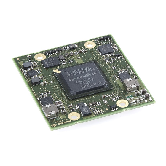
Top and Bottom Views 2.4.1 Top View Figure 4: Module Top View 2.4.2 Bottom View Figure 5: Module Bottom View Please note that depending on the hardware revision and configuration, the module may look slightly dif- ferent than shown in this document. D-0000-421-002 11 / 50 Version 05, 25.07.2019... -
Page 12: Top And Bottom Assembly Drawings
Top and Bottom Assembly Drawings 2.5.1 Top Assembly Drawing Figure 6: Module Top Assembly Drawing 2.5.2 Bottom Assembly Drawing Figure 7: Module Bottom Assembly Drawing Please note that depending on the hardware revision and configuration, the module may look slightly dif- ferent than shown in this document. -
Page 13: Module Footprint
Figure 8: Module Footprint - Top View Warning! It is possible to mount the Mercury CA1 FPGA module the wrong way round on the base board - always check that the mounting holes on the base board are aligned with the mounting holes of the Mercury CA1 FPGA module. -
Page 14: Mechanical Data
Mechanical Data Table 3 describes the mechanical characteristics of the Mercury CA1 FPGA module. A 3D model (PDF) and a STEP 3D model are available [8], [9]. Symbol Value Size 54 mm Component height top 3.0 mm Component height bottom 1.2 mm... -
Page 15: User I/O
User I/O 2.9.1 Pinout Information on the Mercury CA1 FPGA module pinout can be found in the Enclustra Mercury Master Pinout [11], and in the additional document Enclustra Module Pin Connection Guidelines [10]. Warning! Please note that the pin types on the schematics symbol of the module connector and in the Master Pinout document are for reference only. - Page 16 Signal Name Description Dir. Term. Comment IN_B<n>_CLK<x>_<PP>_<p> Differential input clock Each differential input pair clock pair can optionally be used as two single- ended input clocks. For that purpose the 100 termination resistor must be removed. IN_B<n>_CLK<y>_<PP> Single-ended input clock IO_B<n>_L<z>_<PP>_<p>...
-
Page 17: Dual-Purpose Pins
Warning! Using differential signals in single-ended mode may have an effect on other differential signals located in the same FPGA bank. Always check your pinout with Intel Quartus software. Table 6 includes information related to the available I/O types in each I/O bank and to the number of I/Os. Bank 2 Bank 3 Bank 4... -
Page 18: Differential I/Os
The information regarding the length of the signal lines from the FPGA device to the module connector is available in Mercury CA1 FPGA Module IO Net Length Excel Sheet [3]. This enables the user to match the total length of the differential pairs on the base board if required by the application. -
Page 19: Vref Usage
FPGA device, as well as other devices on the Mercury CA1 FPGA module. Do not leave a VREF pin floating when the used I/O standard requires a reference voltage, as this may damage the equipped FPGA device, as well as other devices on the Mercury CA1 FPGA module. 2.9.6... - Page 20 Use only VCC_IO voltages compliant with the equipped FPGA device; any other voltages may damage the equipped FPGA device, as well as other devices on the Mercury CA1 FPGA module. Do not leave a VCC_IO pin floating, as this may damage the equipped FPGA device, as well as other devices on the Mercury CA1 FPGA module.
-
Page 21: Signal Terminations
Power Generation Overview The Mercury CA1 FPGA module uses a 5 - 15 V DC power input for generating the on-board supply voltages (1.2 V, 1.8 V, 2.5 V and 3.3 V). Some of these voltages (2.5 V, 3.3 V) are accessible on the module connector. -
Page 22: Voltage Supply Inputs
Figure 10. 2.10.3 Voltage Supply Inputs Table 12 describes the power supply inputs on the Mercury CA1 FPGA module. The VCC voltages used as supplies for the I/O banks are described in Section 2.9.6. Pin Name Module Connector Pins... -
Page 23: Power Consumption
Logic devices like the Intel Cyclone IV FPGA need cooling in most applications; always make sure the FPGA is adequately cooled. Table 14 lists the heat sink and thermal pad part numbers that are compatible with the Mercury CA1 FPGA module. Details on these parts and additional information that may assist in selecting a suitable heat sink for the Mercury CA1 FPGA module can be found in the Enclustra Modules Heat Sink Application Note [15]. -
Page 24: Clock Generation
2.11 Clock Generation A 50 MHz oscillator is used for the Mercury CA1 FPGA module clock generation. The 50 MHz clock is divided by two and then fed to the FPGA logic and to the Ethernet PHY. The Ethernet PHY generates a 125 MHz reference clock based on the 25 MHz clock, which is further routed to the FPGA. -
Page 25: Ddr2 Sdram
2.14 DDR2 SDRAM The DDR2 SDRAM on the Mercury CA1 FPGA module is connected to FPGA I/O banks 7 and 8. In the stan- dard configuration the DDR bus width is 16-bit. The maximum memory bandwidth on the Mercury CA1 FPGA module is:... -
Page 26: Signal Description
2.14.2 Signal Description Please refer to the Mercury CA1 FPGA Module FPGA Pinout Excel Sheet [4] for detailed information on the DDR2 SDRAM connections. 2.14.3 Termination Warning! No external termination is implemented for the data signals on the Mercury CA1 FPGA module. There- fore, it is strongly recommended to enable the on-die termination (ODT) feature of the DDR2 SDRAM device. -
Page 27: Spi Flash
The SPI flash can be used to store the FPGA bitstream, Nios II application code and other user data. 2.15.1 SPI Flash Type Table 20 describes the memory availability and configuration on the Mercury CA1 FPGA module. Module Flash Type... -
Page 28: Signal Description
Gigabit Ethernet A 10/100/1000 Mbit Ethernet PHY is available on the Mercury CA1 FPGA module, connected to the FPGA via RGMII interface. The 25 MHz clock for the PHY is generated on board from the 50 MHz oscillator. A 125 MHz reference clock generated by the PHY is fed back to the FPGA. -
Page 29: External Connectivity
Table 22: Gigabit Ethernet Signals Description 2.16.3 External Connectivity The Ethernet signal lines can be connected directly to the magnetics. Please refer to the Enclustra Module Pin Connection Guidelines [10] for details regarding the connection of Ethernet signals. 2.16.4 MDIO Address For modules from revision 1 to revision 5 equipped with the Marvell Ethernet PHY, the MDIO address as- signed to the Gigabit Ethernet PHY is 0. -
Page 30: Gigabit Ethernet Phy Configuration
RGMII Delays Configuration The new Ethernet PHY equipped on the Mercury CA1 FPGA module starting with revision 6 requires con- figuration of the RGMII delays in order to achieve the same timing as the Marvell PHY used in the previous revisions. -
Page 31: Ftdi Usb 2.0 Controller
2.17 FTDI USB 2.0 Controller The Mercury CA1 FPGA module features an FTDI USB 2.0 controller, which allows data transfers to a host computer using speeds of up to 40 MB/s. The USB controller is connected to the FPGA module using a synchronous FIFO interface configured for 8-bit mode using an interface clock of 60 MHz. -
Page 32: Real-Time Clock (Rtc)
A real-time clock is connected to the I2C bus. The RTC features a battery-buffered 128 bytes user SRAM and a temperature sensor. See Section 4 for details on the I2C bus on the Mercury CA1 FPGA module. VBAT pin of the RTC is connected to VCC_BAT on the module connector, and can be connected directly to a 3 V battery. -
Page 33: Eeprom Type
Current and Power Monitor A current and power monitor may optionally be equipped on the Mercury CA1 FPGA module to monitor the 1.2 V supply. This circuit is connected to the on-board I2C bus. See Section 4 for details on the I2C bus on the Mercury CA1 FPGA module. -
Page 34: Device Configuration
All configuration signals except for FPGA_MODE must be high impedance as soon as the device is released from reset. Violating this rule may damage the equipped FPGA device, as well as other devices on the Mercury CA1 FPGA module. FPGA Configuration Pins The MSEL pins are used to select an FPGA configuration scheme;... -
Page 35: Configuration Mode
It is recommended to add 22 series termination resistors between the module and the JTAG header, close to the source. Please refer to the Enclustra Module Pin Connection Guidelines for details on JTAG interface. Passive Serial Configuration In the passive serial configuration mode, the bitstream must be transmitted from an external device to the FPGA. -
Page 36: Signal Description
3.4.1 Signal Description Signal Name Description FLASH_DCLK Configuration clock FLASH_DO_FPGA_DI Configuration data FPGA_STATUS# Is pulled low by the FPGA if any CRC error occurs during the configuration; it may be used as an input to delay the start of the FPGA configuration. FPGA_CONFDONE Goes high after a successful FPGA configuration FPGA_CONFIG#... -
Page 37: Signal Description
Table 33: Active Serial Configuration - Signals Description SPI Flash Programming via JTAG The SPI flash device on the Mercury CA1 FPGA module can be programmed via JTAG using different methods: By using Nios II Flash Programmer This option can be used when a Nios II processor is instantiated in the FPGA design It requires the FPGA to be already programmed with an .sof file corresponding to an FPGA design... -
Page 38: Spi Flash Programming From An External Spi Master
Figure 12: SPI Flash Programming from an External SPI Master - Signal Diagrams Warning! Accessing the SPI flash directly without putting the FPGA device into reset may damage the equipped FPGA device, as well as other devices on the Mercury CA1 FPGA module. D-0000-421-002 38 / 50... -
Page 39: Signal Description
3.8.1 Signal Description Signal Name SPI Flash Pin Description FLASH_DCLK SPI CLK FLASH_DO_FPGA_DI SO/IO1 SPI MISO FPGA_CONFIG# Must be pulled low during SPI flash programming. When released, all other pins of the SPI interface must be high impedance. FLASH_DI SI/IO0 SPI MOSI FLASH_CS# SPI CS#... -
Page 40: Fpga Passive Serial Configuration Via Ftdi
The control signals CONFIG_I2C_EN# and CONFIG_EN# are used to configure the way BDBUS0-3 pins are routed on the module: to I2C, SPI flash or FPGA SPI configuration port. Please note that for the SPI flash programming, FPGA_CONFIG# must be pulled to ground. For the passive serial configuration FPGA_MODE must be pulled high or left open, while for active serial configuration FPGA_MODE must be pulled low. -
Page 41: Enclustra Module Configuration Tool
FPGA device, as well as other devices on the Mercury CA1 FPGA module. 3.10 Enclustra Module Configuration Tool The SPI flash on the Mercury CA1 FPGA module can be programmed via FTDI using the Enclustra Module Configuration Tool (MCT) [14]. Passive serial configuration is also supported by the Enclustra MCT software. D-0000-421-002 41 / 50 Version 05, 25.07.2019... -
Page 42: I2C Communication
4 I2C Communication Overview The I2C bus on the Mercury CA1 FPGA module is connected to the FPGA device, EEPROM, RTC and cur- rent and power monitor, and is available on the module connector. This allows external devices to read the module type and to connect more devices to the I2C bus. -
Page 43: Secure Eeprom
Please contact us for further information. Warning! The secure EEPROM is for Enclustra use only. Any attempt to write data to the secure EEPROM causes the warranty to be rendered void. -
Page 44: Product Information
Module Product Family Reserved Revision Product Information Mercury CA1 FPGA module 0x0322 0x[XX] 0x[YY] 0x0322 [XX][YY] Table 42: Product Information Module Configuration Addr. Bits Comment Min. Value Max. Value Comment FPGA Type See FPGA type table (Table 44) 0x08 FPGA device speed grade... - Page 45 Ethernet MAC Address The Ethernet MAC address is stored using big-endian byte order (MSB on the lowest address). Each module is assigned two sequential MAC addresses; only the lower one is stored in the EEPROM. D-0000-421-002 45 / 50 Version 05, 25.07.2019...
-
Page 46: Operating Conditions
5 Operating Conditions Absolute Maximum Ratings Table 45 indicates the absolute maximum ratings for Mercury CA1 FPGA module. The values given are for reference only; for details please refer to the Cyclone IV Datasheet [16]. Symbol Description Rating Unit VCC_IN Supply voltage relative to GND -0.5 to 16... -
Page 47: Ordering And Support
6 Ordering and Support Ordering Please use the Enclustra online request/order form for ordering or requesting information: http://www.enclustra.com/en/order/ Support Please follow the instructions on the Enclustra online support site: http://www.enclustra.com/en/support/ D-0000-421-002 47 / 50 Version 05, 25.07.2019... - Page 48 List of Figures Hardware Block Diagram ........Product Code Fields .
- Page 49 I2C Addresses ..........43 EEPROM Sector 0 Memory Map .
- Page 50 [1] Enclustra General Business Conditions http://www.enclustra.com/en/products/gbc/ [2] Mercury CA1 FPGA Module Reference Design Ask Enclustra for details [3] Mercury CA1 FPGA Module IO Net Length Excel Sheet Ask Enclustra for details [4] Mercury CA1 FPGA Module FPGA Pinout Excel Sheet Ask Enclustra for details...
Need help?
Do you have a question about the Mercury CA1 and is the answer not in the manual?
Questions and answers