Table of Contents
Advertisement
Quick Links
Mars ZX3 SoC Module
Purpose
The purpose of this document is to present the characteristics of Mars ZX3 SoC module to the user, and to
provide the user with a comprehensive guide to understanding and using the Mars ZX3 SoC module.
Summary
This document first gives an overview of the Mars ZX3 SoC module followed by a detailed description of its
features and configuration options. In addition, references to other useful documents are included.
Product Information
Product
Document Information
Reference / Version / Date
Approval Information
Written by
Verified by
Approved by
User Manual
Number
MA-ZX3
Reference
D-0000-424-004
Name
DIUN, GKOE
GLAC
RPAU
Enclustra GmbH – Räffelstrasse 28 – CH-8045 Zürich – Switzerland
Name
Mars ZX3 SoC Module
Version
05
Position
Design Engineer
Technical Expert
Quality Manager
Phone +41 43 343 39 43 – www.enclustra.com
Date
21.08.2018
Date
18.04.2016
27.04.2016
21.08.2018
Advertisement
Chapters
Table of Contents

Related Manuals for Enclustra Mars ZX3


Summary of Contents for Enclustra Mars ZX3
- Page 1 User Manual Purpose The purpose of this document is to present the characteristics of Mars ZX3 SoC module to the user, and to provide the user with a comprehensive guide to understanding and using the Mars ZX3 SoC module. Summary This document first gives an overview of the Mars ZX3 SoC module followed by a detailed description of its features and configuration options.
- Page 2 Unauthorized duplication of this document, in whole or in part, by any means is prohibited without the prior written permission of Enclustra GmbH, Switzerland. Although Enclustra GmbH believes that the information included in this publication is correct as of the date of publication, Enclustra GmbH reserves the right to make changes at any time without notice.
-
Page 3: Table Of Contents
Enclustra Build Environment ........ - Page 4 3.11 Enclustra Module Configuration Tool ........38 I2C Communication Overview .
-
Page 5: Overview
The Enclustra Build Environment [15] is available for the Mars ZX3 SoC module. This build system allows the user to quickly set up and run Linux on any Enclustra SoC module. It allows the user to choose the desired target and download all the required binaries, such as bitstream and FSBL (First Stage Boot Loader). -
Page 6: Electrostatic Discharge
ESD-protected environment. 1.1.7 Electromagnetic Compatibility The Mars ZX3 SoC module is a Class A product and is not intended for use in domestic environments. The product may cause electromagnetic interference, for which appropriate measures must be taken. Features Xilinx Zynq®-7020 All Programmable SoC, CLG484 package... -
Page 7: Accessories
Enclustra Build Environment The Enclustra Build Environment [15] enables the user to quickly set up and run Linux on any Enclustra SoC module. It allows the user to choose the desired target, and download all the required binaries, such as bitstream and FSBL. -
Page 8: Xilinx Tool Support
Please note that the available features depend on the equipped Mars module type. Xilinx Tool Support The SoC devices equipped on the Mars ZX3 SoC module are supported by the Vivado HL WebPACK Edition software, which is available free of charge. Please contact Xilinx for further information. -
Page 9: Module Description
Figure 1: Hardware Block Diagram The main component of the Mars ZX3 SoC module is the Xilinx Zynq-7000 SoC device. Most of its I/O pins are connected to the Mars module connector, making 108 user I/Os available to the user. -
Page 10: Article Numbers And Article Codes
The correspondence between article number and article code is shown in Table 2. The article code repre- sents the product code, followed by the revision; the R suffix and number represent the revision number. The revision changes and product known issues are described in the Mars ZX3 SoC Module Known Issues and Changes document [6]. -
Page 11: Article Numbers And Article Codes
Article Number Article Code EN100021 MA-ZX3-20-1C-D9-R2 EN100022 MA-ZX3-20-2I-D10-R2 EN100079 MA-ZX3-20-2I-D10-R3 EN100080 MA-ZX3-20-1C-D9-R3 EN100915 MA-ZX3-20-1C-D9-R4 EN100916 MA-ZX3-20-2I-D10-R4 EN101311 MA-ZX3-20-1C-D9-R5 EN101312 MA-ZX3-20-2I-D10-R5 EN101493 MA-ZX3-20-1C-D9-R6 EN101494 MA-ZX3-20-2I-D10-R6 EN101556 MA-ZX3-20-1C-D9-R6.1 EN101557 MA-ZX3-20-2I-D10-R6.1 Table 2: Article Numbers and Article Codes D-0000-424-004 11 / 48 Version 05, 21.08.2018... -
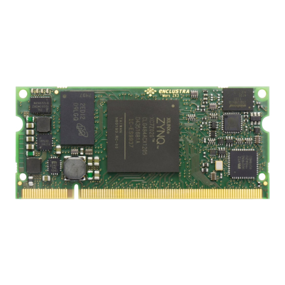
Page 12: Top And Bottom Views
Top and Bottom Views 2.4.1 Top View Figure 4: Module Top View 2.4.2 Bottom View Figure 5: Module Bottom View Please note that depending on the hardware revision and configuration, the module may look slightly dif- ferent than shown in this document. D-0000-424-004 12 / 48 Version 05, 21.08.2018... -
Page 13: Top And Bottom Assembly Drawings
Top and Bottom Assembly Drawings 2.5.1 Top Assembly Drawing Figure 6: Module Top Assembly Drawing 2.5.2 Bottom Assembly Drawing Figure 7: Module Bottom Assembly Drawing Please note that depending on the hardware revision and configuration, the module may look slightly dif- ferent than shown in this document. -
Page 14: Mechanical Data
Module Connector The Mars ZX3 SoC module fits into a 200-pin DDR2 SO-DIMM (1.8 V) socket. Up to four M2 screws may be used to mechanically fasten the module to the base board. Do not use excessive force to tighten the screws, as this could damage the module. -
Page 15: User I/O
User I/O 2.9.1 Pinout Information on the Mars ZX3 SoC module pinout can be found in the Enclustra Mars Master Pinout [11], and in the additional document Enclustra Module Pin Connection Guidelines [10]. The naming convention for the user I/Os is: IO_B<BANK>_L<PAIR><_SPECIAL_FUNCTION>_<PACKAGE_PIN>_<POLARITY>. -
Page 16: Differential I/Os
The information regarding the length of the signal lines from the SoC device to the module connector is available in Mars ZX3 SoC Module IO Net Length Excel Sheet [3]. This enables the user to match the total length of the differential pairs on the base board if required by the application. -
Page 17: Vref Usage
Some of the system pins must be defined as input or high impedance. Please refer to the Mars ZX3 SoC module reference design for details [2]. -
Page 18: Signal Terminations
Internal differential termination is available only for certain VCCO voltages; please refer to Xilinx AR# 43989 for details. Single-Ended Outputs There are no series termination resistors on the Mars ZX3 SoC module for single-ended outputs. If required, series termination resistors may be equipped on the base board (close to the module pins). D-0000-424-004 18 / 48 Version 05, 21.08.2018... -
Page 19: Multiplexed I/O (Mio) Pins
GPIOs; the suggested functions below are for reference only - always verify your MIO pinout with the Xilinx device handbook. Table 9 gives an overview over the MIO pin connections on the Mars ZX3 SoC module. Only the pins marked with “user functionality” are available on the module connector. -
Page 20: Analog Inputs
Power Generation Overview The Mars ZX3 SoC module uses a 3.3 - 5.0 V DC power input for generating the on-board supply voltages (1.0 V, 1.35 V/1.5 V, 1.8 V). These internally-generated voltages are accessible on the module connector. In addition, a separate 3.3 V power input is used to supply peripherals, such as the Ethernet PHY, QSPI flash,... -
Page 21: Power Enable/Power Good
SDRAM unpowered, and detaching the separate 3.3 V power input from the peripherals. The PWR_EN input is pulled to VCC_3V3 on the Mars ZX3 SoC module with a 10 k resistor. The PWR_GOOD signal is pulled to VCC_3V3 on the Mars ZX3 SoC module with a 10 k resistor. -
Page 22: Voltage Supply Outputs
Battery voltage for the RTC and SoC en- cryption key storage Table 13: Voltage Supply Inputs 2.10.4 Voltage Supply Outputs Table 14 presents the supply voltages generated on the Mars ZX3 SoC module, that are available on the module connector. Pin Name Module Connector Pins Voltage... -
Page 23: Heat Dissipation
For Enclustra Mars modules an Enclustra heat sink is available for purchase along with the product. It represents an optimal solution to cool the Mars ZX3 SoC module- it is low profile (less than 7 mm tall) and covers the whole module surface. It comes with a gap pad for the SoC device and four screws to attach it to the module PCB. -
Page 24: Reset
2.14 DDR3 SDRAM There is a single DDR3 SDRAM channel on the Mars ZX3 SoC module attached directly to the PS side and is available only as a shared resource to the PL side. The DDR3 SDRAM is operated at 1.35 V (low power mode) or at 1.5 V, depending on a selection signal. Two 16-bit memory chips are used to build a 32-bit wide memory. -
Page 25: Ddr3 Sdram Type
Other DDR3 memory devices may be equipped in future revisions of the Mars ZX3 SoC module. Please check the user manual regularly for updates. 2.14.2 Signal Description Please refer to the Mars ZX3 SoC Module FPGA Pinout Excel Sheet [4] for detailed information on the DDR3 SDRAM connections. 2.14.3 Termination Warning! No external termination is implemented on the Mars ZX3 SoC module. -
Page 26: Ddr3 Low Voltage Operation
Parameter Value Memory type DDR3/DDR3L DRAM bus width 32 bit Operating frequency 400-533 MHz DRAM chip bus width 16 bit DRAM chip capacity 2048-4096 Mbits Speed bin DDR3_1066F/DDR3L_1066F Bank bits Row bits 14-15 (depending on the module type) Column bits CAS latency CAS write latency RAS to CAS delay... -
Page 27: Qspi Flash Type
512 bytes instead of 256 bytes. This may require adjustments of the programming algorithm. As there is one QSPI flash chip equipped on the Mars ZX3 SoC module, type “single” must be selected when programming the flash from Vivado tools. -
Page 28: Nand Flash
Please refer to the NAND flash memory device datasheet to extract the required parameter values. Refer- ence values to be used in Vivado are given in Table 24. The indicated parameter values may be used for booting from NAND flash memory on the Mars ZX3 SoC module. -
Page 29: Sd Card
An SD card can be connected to the PS MIO pins 40-45 or 46-51, or alternatively via EMIO pins to the PL. The corresponding MIO pins are available on the module connector. Note that only MIO pins 40-45 allow the Mars ZX3 SoC module to boot from the SD card. Information on this boot mode is available in Section 3.6. -
Page 30: Signal Description
Table 26: Gigabit Ethernet Signal Description 2.18.3 External Connectivity The Ethernet signal lines can be connected directly to the magnetics. Please refer to the Enclustra Module Pin Connection Guidelines [10] for details regarding the connection of Ethernet signals. 2.18.4 MDIO Address The MDIO address assigned to the Gigabit Ethernet PHY is 3. -
Page 31: Phy Configuration
MHz. 2.19 USB 2.0 The Mars ZX3 SoC module has an on-board USB 2.0 PHY connected to the SoC device. The USB interface can be configured for USB host, USB device and USB On-The-Go (host and device capable) operations. 2.19.1 USB PHY Type Table 28 describes the equipped USB PHY device type on the Mars ZX3 SoC module. -
Page 32: Rtc Type
Manufacturer ISL12020M Intersil Table 29: RTC Type An example demonstrating how to use the RTC is included in the Mars ZX3 SoC module reference design [2]. 2.21 Secure EEPROM The secure EEPROM is used to store the module type and serial number, as well as the Ethernet MAC address and other information. -
Page 33: Device Configuration
3 Device Configuration Configuration Signals The PS of the SoC needs to be configured before the FPGA logic can be used. Xilinx Zynq devices need special boot images to boot from QSPI flash or SD card. For more information, please refer to the Xilinx Zynq-7000: Concepts, Tools, and Techniques document [20]. -
Page 34: Pull-Up During Configuration
For details on the PUDC signal please refer to the Zynq-7000 All Programmable SoC Technical Reference Manual [18]. Boot Mode The boot mode can be selected via a signal available on the module connector. Table 33 describes the available boot modes on the Mars ZX3 SoC module. BOOT_MODE Description Boot from QSPI flash... -
Page 35: Jtag Boot Mode
3.3.1 JTAG Boot Mode For JTAG boot mode selection, the following steps must be followed: BOOT_MODE must be set to logic low MIO5 (NAND_IO0/FLASH_IO3) must be pulled to GND (refer to Table 34 for details) Module Hardware changes required to pull MIO5 to GND MA-ZX3 - R1 R111 must be mounted MA-ZX3 - R2 and R3... -
Page 36: Jtag On Module Connector
It is recommended to add 22 series termination resistors between the module and the JTAG header, close to the source. Please refer to the Enclustra Module Pin Connection Guidelines for details on JTAG interface. QSPI Boot Mode In the QSPI boot mode, the PS boots from the QSPI flash located on the module. The flash device is con- nected to the PS MIO pins 1-6. -
Page 37: Qspi Flash Programming From An External Spi Master
SoC device, as well as other devices on the Mars ZX3 SoC module. NAND Flash Programming The NAND flash on the Mars ZX3 SoC module can be programmed via JTAG or from u-boot. The Xilinx SDK software offers NAND flash programming support via JTAG. For the programming operation, type “nand_8”... -
Page 38: Fpga And Qspi Flash Programming Using Xilinx Impact
For Zynq-7000 devices, Xilinx Impact requires JTAG boot mode to be selected in order to download the bitstream or program the QSPI flash. As this operation on the Mars ZX3 SoC module requires hardware changes (please refer to Section 3.3.1), it is recommended to use Xilinx SDK or Vivado for FPGA or QSPI flash programming. -
Page 39: I2C Communication
Overview The I2C bus on the Mars ZX3 SoC module is connected to the SoC device, EEPROM and RTC, and is available on the module connector. This allows external devices to read the module type and to connect more devices to the I2C bus. -
Page 40: I2C Address Map
An example demonstrating how to read the module information from the EEPROM memory is included in the Mars ZX3 SoC module reference design. Warning! The secure EEPROM is for Enclustra use only. Any attempt to write data to the secure EEPROM causes the warranty to be rendered void. 4.4.1... -
Page 41: Product Information
Module Product Information This field indicates the type of module and hardware revision. Module Product Family Reserved Revision Product Information Mars ZX3 SoC module 0x0323 0x[XX] 0x[YY] 0x0323 [XX][YY] Table 39: Product Information Module Configuration Addr. Bits Comment Min. Value Max. - Page 42 Ethernet MAC Address The Ethernet MAC address is stored using big-endian byte order (MSB on the lowest address). Each module is assigned two sequential MAC addresses; only the lower one is stored in the EEPROM. D-0000-424-004 42 / 48 Version 05, 21.08.2018...
-
Page 43: Operating Conditions
5 Operating Conditions Absolute Maximum Ratings Table 42 indicates the absolute maximum ratings for Mars ZX3 SoC module. The values given are for refer- ence only; for details please refer to the Zynq-7000 DC and AC Switching Characteristics Datasheet [23]. -
Page 44: Recommended Operating Conditions
Recommended Operating Conditions Table 43 indicates the recommended operating conditions for Mars ZX3 SoC module. The values given are for reference only; for details please refer to the Zynq-7000 DC and AC Switching Characteristics Datasheet [23]. Symbol Description Rating Unit... -
Page 45: Ordering And Support
6 Ordering and Support Ordering Please use the Enclustra online request/order form for ordering or requesting information: http://www.enclustra.com/en/order/ Support Please follow the instructions on the Enclustra online support site: http://www.enclustra.com/en/support/ D-0000-424-004 45 / 48 Version 05, 21.08.2018... - Page 46 List of Figures Hardware Block Diagram ........Product Code Fields .
- Page 47 Product Information ......... . . 41 Module Configuration .
- Page 48 [1] Enclustra General Business Conditions http://www.enclustra.com/en/products/gbc/ [2] Mars ZX3 SoC Module Reference Design Ask Enclustra for details [3] Mars ZX3 SoC Module IO Net Length Excel Sheet Ask Enclustra for details [4] Mars ZX3 SoC Module FPGA Pinout Excel Sheet Ask Enclustra for details...
Need help?
Do you have a question about the Mars ZX3 and is the answer not in the manual?
Questions and answers