Table of Contents
Advertisement
Quick Links
Andromeda XZU65 Module
Purpose
The purpose of this document is to present the characteristics of Andromeda XZU65 module to the user,
and to provide the user with a comprehensive guide to understanding and using the Andromeda XZU65
module.
Summary
This document first gives an overview of the Andromeda XZU65 module followed by a detailed descrip-
tion of its features and configuration options. In addition, references to other useful documents are
included.
Product Information
Product
Document Information
Reference / Version / Date
Approval Information
Written by
Verified by
Approved by
User Manual
Code
AM-XZU65
Reference
D-0000-483-001
Name
MGOS
MKON
SJOK
Enclustra GmbH – Räffelstrasse 28 – CH-8045 Zürich – Switzerland
Name
Andromeda XZU65 Module
Version
01
Position
Technical Writer
Design Expert
Manager, BU SP
Phone +41 43 343 39 43 – www.enclustra.com
Date
13.03.2023
Date
13.03.2023
13.03.2023
13.03.2023
Advertisement
Chapters
Table of Contents

Related Manuals for Enclustra Andromeda XZU65


Summary of Contents for Enclustra Andromeda XZU65
- Page 1 Andromeda XZU65 Module User Manual Purpose The purpose of this document is to present the characteristics of Andromeda XZU65 module to the user, and to provide the user with a comprehensive guide to understanding and using the Andromeda XZU65 module.
- Page 2 Unauthorized duplication of this document, in whole or in part, by any means is prohibited without the prior written permission of Enclustra GmbH, Switzerland. Although Enclustra GmbH believes that the information included in this publication is correct as of the date of publication, Enclustra GmbH reserves the right to make changes at any time without notice.
-
Page 3: Table Of Contents
Enclustra Build Environment ........ - Page 4 3.12 Enclustra Module Configuration Tool ....... . . 48 D-0000-483-001 4 / 60 Version 01, 13.03.2023...
- Page 5 I2C Communication Overview ..........49 Signal Description .
-
Page 6: Overview
DDR channels. The use of the Andromeda XZU65 module, in contrast to building a custom MPSoC hardware, significantly reduces development effort and redesign risk and improves time-to-market for the embedded system. -
Page 7: Electrostatic Discharge
1.1.7 Electromagnetic Compatibility The Andromeda XZU65 module is a Class A product (as defined in IEC 61000-3-2 standard) and is not intended for use in domestic environments. The product may cause electromagnetic interference, for which appropriate measures must be taken. -
Page 8: Deliverables
1.3.3 Petalinux BSP The Enclustra Petalinux BSPs enable the user to quickly set up a Petalinux project and to run Linux on the Enclustra SoC module or system board. The documentation [14] describes the build process in detail and allows a user without Petalinux knowl- edge to build and run the desired design on the target hardware. -
Page 9: Accessories
Accessories 1.4.1 Enclustra Heat Sink An Enclustra heat sink is available for the Andromeda XZU65 module. Refer to Section 2.10.6 for further information on the available cooling options. 1.4.2 Andromeda-Mercury ADA1 Adapter The Andromeda-Mercury ADA1 adapter is an adapter board to connect an Andromeda XZU65 module to a Mercury ST1 base board. -
Page 10: Module Description
Connector Y Figure 1: Hardware Block Diagram The main component of the Andromeda XZU65 module is the Xilinx Zynq UltraScale+ MPSoC device. Most of its I/O pins are connected to the Andromeda module connector, making up to 322 regular user I/Os available to the user. -
Page 11: Module Configuration And Product Models
Figure 2: Product Model Fields Please note that for the first revision modules or early access modules, the product model may not respect entirely this naming convention. Please contact Enclustra for details on this aspect. D-0000-483-001 11 / 60... -
Page 12: Numbers And Product Models
Figure 3: Module Label The correspondence between EN-number and product model for each revision is shown in Table 2. The revision changes and product known issues are described in the Andromeda XZU65 Module Known Issues and Changes document [6]. EN-Number... -
Page 13: Top And Bottom Views
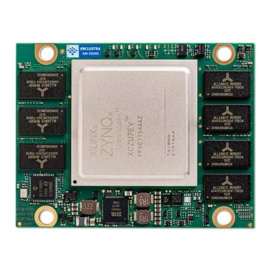
Top and Bottom Views 2.4.1 Top View Figure 4: Module Top View 2.4.2 Bottom View Figure 5: Module Bottom View Please note that depending on the hardware revision and configuration, the module may look slightly different than shown in this document. D-0000-483-001 13 / 60 Version 01, 13.03.2023... -
Page 14: Top And Bottom Assembly Drawings
Top and Bottom Assembly Drawings 2.5.1 Top Assembly Drawing R1709 Q1900 Q1901 Z2303 R1902 R1538 R1537 R504 R1340 R1339 C1514 C1513 R502 C1501 C1314 C1505 R1402 R1403 C1506 C1517 C1527 C1313 C1303 C1301 R1531 R1532 C1504 C1316 C1327 U1300 U1401 C1325 R501 U1201... -
Page 15: Module Footprint And Mechanical Data
The maximum component height under the module is dependent on the connector type - refer to Section 2.7 for detailed connector information. Figure 8: Module Footprint and Dimensionss - Top View Table 3 describes the mechanical characteristics of the Andromeda XZU65 module. A 3D model (PDF) and a STEP 3D model are available [8], [9]. Parameter... -
Page 16: Pin Numbering For The Module Connector
Reference Type Description Andromeda module connector ADM6-60-01.5-L-4-2 Samtec ADM6, 240-pin, 0.635 mm pitch Base board connector ADF6-60-03.5-L-4-2 Samtec ADM6, 240-pin, 0.635 mm pitch, 5 mm stacking height Table 4: Module Connector Types Connector W: J200 A1-A60, B1-B60, C1-C60, D1-D60 Connector X: J300 A1-A60, B1-B60, C1-C60, D1-D60 Connector Y: J400 A1-A60, B1-B60, C1-C60, D1-D60 Figure 9: Pin Numbering for the Module Connector NOTICE... -
Page 17: User I/O
2.8.1 Pinout Information on the Andromeda XZU65 module pinout can be found in the Enclustra Andromeda Master Pinout [11], and in the additional document Enclustra Module Pin Connection Guidelines [10]. The pin types on the schematic of the module connector and in the Master Pinout document are for reference only. -
Page 18: I/O Pin Exceptions
The I/O pin exceptions are pins with special functions or restrictions (for example, when used in combi- nation with certain Andromeda boards they may have a specific role). PCIe Reset Signal (PERST#) Table 6 lists the I/O pin exceptions on the Andromeda XZU65 module related to the PCIe reset connection. I/O Name Module Connector Pin... -
Page 19: Differential I/Os
The information regarding the length of the signal lines from the MPSoC device to the module connector is available in Andromeda XZU65 Module IO Net Length Excel Sheet [3]. This enables the user to match the total length of the differential pairs on the base board if required by the application. -
Page 20: V_Io Usage
V_IO_B[x], respectively V_IO_CFG pins. All V_IO_B[x] or V_IO_CFG pins of the same bank must be connected to the same voltage. For compatibility with other Enclustra Andromeda modules, it is recommended to use a single I/O voltage per module connector. -
Page 21: Signal Terminations
NOTICE Damage to the device due to unsuitable voltage Unsuitable voltages may damage the MPSoC device as well as other devices on the Andromeda XZU65 module. Only use V_IO voltages compliant with the assembled MPSoC device. NOTICE Damage to the device due to floating V_IO pins Floating V_IO pins reduce ESD protection. -
Page 22: Multiplexed I/O (Mio) Pins
GPIOs; the suggested functions below are for reference only - always verify your MIO pinout with the Xilinx device handbook. Table 9 gives an overview over the MIO pin connections on the Andromeda XZU65 module. Only the pins marked with “user functionality” are available on the module connector. -
Page 23: Analog Inputs
MIO Group Default Function Connection QSPI0 flash QSPI0 flash QSPI feedback clock 7-12 QSPI1 flash QSPI1 flash 13-22 eMMC flash eMMC flash 23-25 User I2C Module connector, can optionally be connected to PL buck converters (not default) UART0 RX /user functionality Module connector UART0 TX /user functionality... -
Page 24: Multi-Gigabit Transceiver (Mgt)
Note that Samtec module connector has a performance limit of 25 Gbit/s for NRZ encoding. GTH Transceivers There are 20 GTH MGTs available on the Andromeda XZU65 module organized in 5 FPGA banks. Table 12 describes the connections. The naming convention for the GTH MGT I/Os is: MGT_B<BANK_LETTER>_<FUNCTION>_<POLARITY>. -
Page 25: Mgt Gth Pairs
6 reference input clock differential pairs are routed to module connector Y. GTR Transceivers There are four GTR MGT pairs and two reference input clock differential pairs on the Andromeda XZU65 module connected to I/O bank 505; these are routed to module connector X. -
Page 26: Power
The maximum data rate on the MGT lines on the Andromeda XZU65 module depends on the routing path for these signals. When using MGTs at high performance rates, ensure adequate signal integrity over the full signal path. NOTICE Damage to the MGT lines No AC coupling capacitors are placed on the Andromeda XZU65 module on the MGT lines. -
Page 27: Generated Pl Power Supplies
DC/DC converters can be configured to generate the required voltages for MPSoC as specified in the Xilinx documentation. Please refer to the Enclustra Module Pin Connection Guidelines for general rules on the power pins [10]. Power Converter Synchronization Some switching converters used on the Andromeda XZU65 module support synchronization of the switch- ing frequency with an external clock. -
Page 28: Power Enable/Power Good
PS and PL supplies separately. By default, PWR_EN_PL is generated from PWR_EN signal (acting as a global enable signal), and PWR_GOOD reflects the general power good status for both PS and PL sides. The signals are pulled to V_3V3_PL/PS on the Andromeda XZU65 module with a 4.7 k resistor. -
Page 29: Voltage Supply Inputs
Do not leave V_IO pins floating. 2.10.3 Voltage Supply Inputs Table 16 describes the power supply inputs on the Andromeda XZU65 module. The voltages used as supplies for the I/O banks are described in Section 2.8.5. Pin Name Module Connector Pins... -
Page 30: Power Consumption
For Andromeda modules an Enclustra heat sink kit is available for purchase along with the product. It represents an optimal solution to cool the Andromeda XZU65 module - the heat sink body is low profile and usually covers the whole module surface. The kit comes with a gap pad for the MPSoC device, a fan and required mounting material to attach the heat sink to the module PCB and baseboard PCB. -
Page 31: Voltage Monitoring
2.11 Clock Generation A 33.333 MHz oscillator is used for the Andromeda XZU65 module clock generation; the 33.333 MHz clock is fed to the PS. For the PL side, an additional 33.333 MHz oscillator is connected to HD bank N. -
Page 32: Reset
Pulling PS_POR# low resets the MPSoC device, the PS Ethernet and the USB PHYs, the QSPI and eMMC flash devices and the secure EEPROM. Please refer to the Enclustra Module Pin Connection Guidelines [10] for general rules regarding the connection of reset pins. -
Page 33: Leds
Please note that all reset signals are automatically asserted if PWR_GOOD is low. 2.13 LEDs There are four active-low user LEDs on the Andromeda XZU65 module - two of them are connected to the PS and two are connected to the PL. Signal Name... -
Page 34: Ddr4 Sdram Characteristics
16 bit Table 23: DDR4 SDRAM (PS) Characteristics 2.14.2 Signal Description Please refer to the Andromeda XZU65 Module FPGA Pinout Excel Sheet [4] for detailed information on the DDR4 SDRAM connections. 2.14.3 Termination No external termination is implemented for the data signals on the Andromeda XZU65 module. Enclus- tra strongly recommends enabling the on-die termination (ODT) feature of the DDR4 SDRAM device. -
Page 35: Ddr4 Sdram (Pl)
64-bit. The DDR4 SDRAM memory controller on the MPSoC device supports speeds up to 2666 Mbit/s (1333 MHz), however the memories assembled on the Andromeda XZU65 module are rated 2400 Mbit/s (1200 MHz). The maximum PL memory bandwidth on the Andromeda XZU65 module is: 2400 Mbit/sec 64 bit = 19’200 MB/sec... -
Page 36: Ddr4 Sdram Characteristics
16 bit Table 25: DDR4 SDRAM (PL) Characteristics 2.15.2 Signal Description Please refer to the Andromeda XZU65 Module FPGA Pinout Excel Sheet [4] for detailed information on the DDR4 SDRAM connections. 2.15.3 Termination No external termination is implemented for the data signals on the Andromeda XZU65 module. Enclus- tra strongly recommends enabling the on-die termination (ODT) feature of the DDR4 SDRAM device. -
Page 37: Qspi Flash Characteristics
QSPI Flash Characteristics Table 27 describes the memory availability and configuration on the Andromeda XZU65 module. As the Andromeda XZU65 module is equipped with two QSPI flash chips, type “dual parallel” must be selected when programming the flash from Vivado tools. -
Page 38: Emmc Flash Characteristics
V_IO_CFG, a level shifter to 3.3 V may be required (some level shifters also have built-in pull-ups). SD version 3.0 is supported on Andromeda XZU65 module. In this case, an SD 3.0 compliant level shifter is required on the base board and V_IO_CFG must be set to 1.8 V. For further information on the SD Card interface please refer to [17]. -
Page 39: Mdio Address
RX and TX data, it is recommended to adjust the pad skew delays as specified in Table 30. These values have been successfully tested on Enclustra side. The delays can be adjusted by programming the RGMII pad skew registers of the Ethernet PHY; please refer to the PHY datasheet for details. -
Page 40: Gigabit Ethernet (Pl)
Please note that the Xilinx GMII to RGMII converter cannot be used on the Andromeda XZU65 module because this IP core includes I/O delay macros that are not supported in HD I/O banks (where the Ethernet pins are mapped). -
Page 41: Rgmii Delays Configuration
2 ns delay on the TX clock signal. 2.21 USB 2.0 A USB 2.0 PHY is available on the Andromeda XZU65 module and connected to the PS to MIO bank 502. The USB PHY can be configured to host, device or On-The-Go (OTG) mode. 2.21.1 USB PHY Characteristics Table 33 describes the USB PHY device that is assembled on the Andromeda XZU65 module. -
Page 42: Display Port
Zynq UltraScale+ devices include an internal real-time clock. More information on the RTC is available in the Zynq UltraScale+ MPSoC Technical Reference Manual [17]. The RTC crystal pad input and crystal pad output are connected on the Andromeda XZU65 module to a 32.768 kHz oscillator. -
Page 43: Secure Eeprom
An example demonstrating how to read data from the EEPROM is included in the Andromeda XZU65 module reference design [2]. This device is connected in parallel to the same I2C bus. It is currently not used by Enclustra and is reserved for future use. D-0000-483-001 43 / 60 Version 01, 13.03.2023... -
Page 44: Device Configuration
3 Device Configuration Configuration Signals The PS of the MPSoC needs to be configured before the FPGA logic can be used. Xilinx Zynq devices need special boot images to boot from QSPI flash, eMMC flash or SD card. For more information, please refer to the Zynq UltraScale+ MPSoC Technical Reference Manual [17]. -
Page 45: Power-On Reset Delay Override
Figure 12 illustrates the configuration of the I/O signals during power-up. Figure 13 indicates the location of the pull-up/pull-down resistors on the module PCB - lower right part on the bottom view drawing. Figure 12: Pull-Up During Configuration (PUDC) and Power-on Reset Delay Override (PORSEL) Figure 13: Pull-Up During Configuration (PUDC) and Power-on Reset Delay Override (PORSEL) Resistors For details on the PUDC signal please refer to the Zynq UltraScale+ MPSoC Technical Reference Manual [17]. -
Page 46: Boot Mode
For details on the POR_OVERRIDE signal please refer to the Zynq UltraScale+ MPSoC Technical Reference Manual [17]. Boot Mode The boot mode can be selected via four signals available on the module connector. Table 36 describes the available boot modes on the Andromeda XZU65 module. BOOT BOOT BOOT... -
Page 47: External Connectivity
The VREF pin of the programmer must be connected to V_IO_CFG. It is recommended to add 22 series termination resistors between the module and the JTAG header, close to the source. Please refer to the Enclustra Module Pin Connection Guidelines for details on JTAG interface. eMMC Boot Mode In the eMMC boot mode, the PS boots from the eMMC flash located on the module. -
Page 48: Qspi Flash Programming Via Jtag
3.12 Enclustra Module Configuration Tool When used in combination with an Enclustra base board, the QSPI flash can be programmed using En- clustra Module Configuration Tool (MCT) [15]. For this method, a non-QSPI boot mode must be used during QSPI flash programming. The entire procedure is described in the reference design documenta- tion. -
Page 49: I2C Communication
4 I2C Communication Overview There are two I2C buses on the Andromeda XZU65 module. They are referred to as “I2C_USER” and “I2C_MGMT”. They are connected to the MPSoC device, the EEPROM, the power converters and to the module connector. This allows external devices to read the module type from the EEPROM and allows connecting more devices to the I2C bus. -
Page 50: I2C Address Map
Enclustra Module PS MIO I2C_MGMT_PS I2C_MGMT Level Shift Bank USER PS Buck FRAM EEPROM Converter (optional) PS MIO I2C_USER_PS I2C_USER Bank Level Shift HD N I2C_PL I2C_USER PL Buck I2C_BC Bank Converter Figure 14: I2C Interface Overview Signal Name PS Pin... -
Page 51: Secure Eeprom
ROM will be used for copy protection and licensing features. Please contact us for further information. An example demonstrating how to read the module information from the EEPROM memory is included in the Andromeda XZU65 module reference design. Any attempt to write data to the secure EEPROM causes the warranty to be rendered void. -
Page 52: Product Information
(MSB on the lowest address). Module Product Information This field indicates the type of module and hardware revision. Module Product Family Reserved Revision Product Information Andromeda XZU65 module 0x033A 0x[XX] 0x[YY] 0x033A [XX][YY] Table 41: Product Information D-0000-483-001 52 / 60... -
Page 53: Module Configuration
Module Configuration Addr. Bits Comment Min. Value Max. Value Comment MPSoC type See MPSoC type table (Table 43) 0x08 MPSoC device speed grade Temperature range See temperature range table (Table 44) Power grade 0 (Normal) 1 (Low power) Gigabit Ethernet port count 0x09 QSPI flash interface See QSPI flash type... -
Page 54: Module Temperature Range
Value Module Temperature Range Commercial Extended Industrial Table 44: Module Temperature Range Table 45 shows the QSPI interface configuration options. Value Interface Type Single Dual parallel Dual stacked Table 45: QSPI flash interface Ethernet MAC Address The Ethernet MAC address is stored using big-endian byte order (MSB on the lowest address). Each module is assigned two sequential MAC addresses;... -
Page 55: Operating Conditions
5 Operating Conditions Absolute Maximum Ratings Table 46 indicates the absolute maximum ratings for Andromeda XZU65 module. The values given are for reference only; for details please refer to the Zynq UltraScale+ MPSoC, DC and AC Switching Charac- teristics Datasheet [19]. -
Page 56: Recommended Operating Conditions
Recommended Operating Conditions Table 47 indicates the recommended operating conditions for Andromeda XZU65 module. The values given are for reference only; for details please refer to the Zynq UltraScale+ MPSoC, DC and AC Switching Characteristics Datasheet [19]. Symbol Description Rating... -
Page 57: Ordering And Support
6 Ordering and Support Ordering Please use the Enclustra online request/order form for ordering or requesting information: http://www.enclustra.com/en/order/ Support Please follow the instructions on the Enclustra online support site: http://www.enclustra.com/en/support/ D-0000-483-001 57 / 60 Version 01, 13.03.2023... - Page 58 List of Figures Hardware Block Diagram ........10 Product Model Fields .
- Page 59 I2C Signal Description ......... . 50 I2C Addresses .
- Page 60 [1] Enclustra General Business Conditions http://www.enclustra.com/en/products/gbc/ [2] Andromeda XZU65 Module Reference Design https://github.com/enclustra [3] Andromeda XZU65 Module IO Net Length Excel Sheet Ask Enclustra for details [4] Andromeda XZU65 Module FPGA Pinout Excel Sheet Ask Enclustra for details [5] Andromeda XZU65 Module User Schematics...
Need help?
Do you have a question about the Andromeda XZU65 and is the answer not in the manual?
Questions and answers