
Subscribe to Our Youtube Channel
Related Manuals for GE Mini COM Express 10


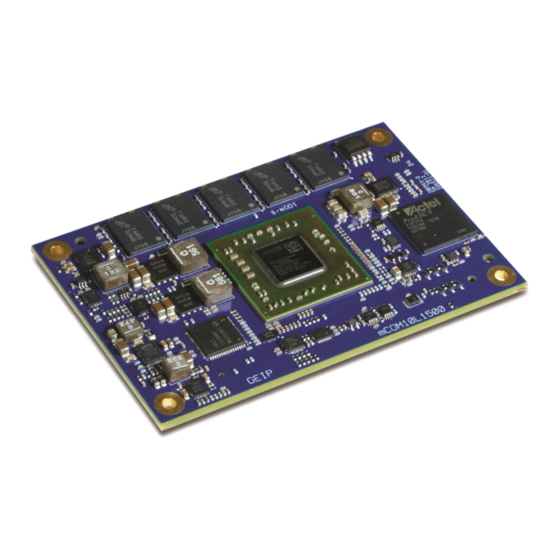
Summary of Contents for GE Mini COM Express 10
- Page 1 GFK-2896 Intelligent Platforms Mini COM Express Type 10 Module mCOM10-L1500 Hardware Reference Manual For public disclosure...
- Page 2 It is understood that GE may make changes, modifications, or improvements to the equipment referenced herein or to the document itself at any time. This document is intended for trained personnel familiar with the GE products referenced herein.
- Page 3 Acronyms and Abbreviations ACPI Advanced Configuration and Power Interface APIC Advanced Programmable Interrupt Controller AT Attachment BIOS Basic Input/Output System Built-In Test Computer on Module Central Processing Unit DDR3 SDRAM Third-Generation Double Data Rate Synchronous Dynamic RAM Direct Memory Access DIMM Dual In-line Memory Module DisplayPort...
- Page 4 SIMD Single Instruction, Multiple Data Stock-keeping unit SMBus System Management Bus System Management Interrupt Serial Presence Detect Serial Peripheral Interconnect SR-IOV Single Root I/O Virtualization Test Access Port Thermal Design Power Trusted Platform Module UART Universal Asynchronous Receiver/Transmitter UDIMM Unbuffered DIMM UEFI Unified EFI UHCI...
- Page 5 Safety Symbol Legend Indicates a procedure, condition, or statement that, if not strictly observed, could result in personal injury or death. Warning Indicates a procedure, condition, or statement that, if not strictly observed, could result in damage to or destruction of equipment.
- Page 6 Warranty ge-ip.com/. The manufacturer grants the original purchaser of GE Intelligent Platforms products a warranty of 24 months from the date of delivery. For details regarding this warranty, refer to the Terms and Conditions of the initial sale. Support The GE Intelligent Platforms’...
-
Page 7: Table Of Contents
Contents 1 Introduction ............................. 11 1.1 Features ............................... 12 2 Unpacking and Inspection ......................15 2.1 Electrostatic Discharge ........................... 15 2.2 Package Contents........................... 16 2.3 Unpacking and Inspecting ........................16 2.4 Handling .............................. 17 3 Installation and Startup......................... 19 3.1 Required Materials..........................19 3.1.1 Carrier Board and Power Supply ...................... - Page 8 4.7 LED Status Indicators..........................30 5 Configuration........................... 31 5.1 Hardware ............................. 31 5.1.1 COM Express Type 10 Module Connectors..................31 5.1.2 JTAG Connector ..........................40 5.1.3 PCIe Ports ............................. 41 5.2 Software .............................. 42 5.2.1 Memory and I/O Address Mapping..................... 42 5.2.2 SMBus Slave Devices........................
- Page 9 6.7.7 Modem Control ..........................61 6.7.8 Line Status............................. 62 6.7.9 Modem Status ..........................63 6.7.10 Scratchpad............................. 64 6.7.11 Divisor Latch ..........................64 6.8 Board Supervision Run-Time Registers...................... 65 6.8.1 Reset Cause ........................... 65 6.8.2 Last Reset............................66 6.9 I C Controller Run-Time Registers......................67 6.9.1 Clock Prescale..........................
- Page 10 Notes GFK-2896 Mini COM Express Type 10 Module mCOM10-L1500 For public disclosure...
-
Page 11: Introduction
1 Introduction The mCOM10-L1500 is a miniature Computer-on-Module (mCOM) Type 10 single-board computer approximately the size of a credit card, based on an AMD G-Series System-on-chip (SoC). It contains one channel of DDR3L 72-bit ECC memory and all components necessary for the bootable host computer packaged as a super component. -
Page 12: Features
1.1 Features The mCOM10-L1500 provides the following core hardware and firmware features: • AMD G-Series SoC, including: − Two or four CPU cores − GPU core − Northbridge − DDR3 memory controller − Integrated display output − I/O controller − Dual-core 9W TDP and quad-core 15W TDP SKUs available •... - Page 13 G-Series SoC FPGA User Supv Ser0 CPU Core UART CPU Core CPU Core CPU Core Ser1 L1 Cache L1 Cache EeeP UART L1 Cache L1 Cache WDog L2 Cache LVDS/eDP DDR3 L North Bridge DDI0 2 /4/8GB PCIe GbE0 I210 PCIe[0:3] SMBus Debug...
- Page 14 Notes GFK-2896 Mini COM Express Type 10 Module mCOM10-L1500 For public disclosure...
-
Page 15: Unpacking And Inspection
2 Unpacking and Inspection This chapter describes unpacking, initial inspection, and required preparation considerations prior to using the mCOM10-L1500. Follow the procedures provided in this chapter to verify proper operation after shipping and prior to system integration. 2.1 Electrostatic Discharge Electrostatic Discharge (ESD), the discharge of static electricity, is a major cause of electronic component failure. -
Page 16: Package Contents
If evidence of damage or rough handling is found, notify the shipping service and GE Intelligent Platforms as soon as possible. GFK-2896 Mini COM Express Type 10 Module mCOM10-L1500... -
Page 17: Handling
2.4 Handling Proper handling of the board or module is critical to ensure proper operation and long-term reliability. When unpacking and handling the board, be sure to hold the board as displayed in the following figure. Board Handling Unpacking and Inspection GFK-2896 Hardware Reference Manual 17 For public disclosure... - Page 18 Notes GFK-2896 Mini COM Express Type 10 Module mCOM10-L1500 For public disclosure...
-
Page 19: Installation And Startup
3 Installation and Startup This chapter describes the installation of the mCOM10-L1500 module on a carrier board and initial startup operations. 3.1 Required Materials The following items are required to start the board in a standard configuration: • Carrier board and power supply •... -
Page 20: General Installation Guidelines
3.2 General Installation Guidelines Adhere to the following guidelines during installation: • Observe all safety procedures to avoid damaging the system and protect operators and users. • Before installing or removing any board, verify that the system power and external supplies have been turned off. -
Page 21: Installation Procedures
3.3 Installation Procedures 3.3.1 Install the mCOM10-L1500 onto the Carrier Board A carrier board with a matching connector is required. Refer to the carrier board manual. � � To install the mCOM10-L1500 onto the carrier board Carefully slide the mCOM10-L1500 board onto the connector on the carrier board. Fasten the mCOM10-L1500 to the board using four M2.5 screws. -
Page 22: Install The Combined Unit
3.4.1 UEFI Firmware Setup � � To enter setup during the initial startup sequence: press the Delete or F2 Contact GE Intelligent during the boot up sequence. Adhere to the applicable on-screen messages when Platforms for technical prompted. -
Page 23: System Architecture
4 System Architecture This chapter describes the features, capabilities, and compatibilities of the mini COM Express Type 10 module. 4.1 G-Series SoC Processor The main component of the mCOM10-L1500 is the AMD G-Series SoC, which integrates the following functions: • Two or four processor cores •... -
Page 24: Memory
4.1.1 Memory The main memory array contains one channel of 72-bit wide DDR3L SDRAM, with optional 2 GB, 4 GB, or 8 GB density. The system memory controller is integrated in the G-Series SoC processor. A Serial Presence Detect (SPD) EEPROM, attached to the internal SMBus, provides memory configuration information to the boot firmware. -
Page 25: Bios/Uefi Firmware
4.1.4 BIOS/UEFI Firmware Refer to PICMG COM.0 R2.1 The mCOM10-L1500 has an on-board 8 MByte SPI Flash ROM device that holds the COM Express Module Base BIOS/UEFI firmware load. Alternatively, the module may be configured to boot from the Specification located at Flash located on the carrier board, on either the external SPI bus or LPC bus. -
Page 26: Clocks
4.1.9 Clocks Most of the system clocks are generated from a 48 MHz crystal by an integrated clock generator within the G-Series SoC. The following clock groups are provided by the clock generator: Internal clocks are supplied to the CPU cores, cache, GPU, peripheral controllers, and the intra-chip buses. -
Page 27: Gigabit Ethernet Interface
4.2 Gigabit Ethernet Interface The mCOM10-L1500 provides one 10/100/1000 Mbps MDI through an Intel I210 Gigabit Ethernet Controller. The I210 controller supports the following features: • Jumbo frames up to 9.5 KB • 802.1q VLAN • 64-bit addressing • IEEE 1588 time synchronization (per-packet timestamp) The I210 MDI port is wired directly to the COM Express connector. -
Page 28: Fpga
4.3 FPGA Refer to Chapter, FPGA The mCOM10-L1500 includes an FPGA that provides board supervision with control of Registers. the powerup, power down, and reset sequencing. It also contains the watchdog timer, I²C controller, and two UARTS. System interface is provided through the LPC bus. 4.3.1 Watchdog Timer The FPGA provides a dedicated two-stage watchdog timer (WDT) for the mCOM10-L1500 processor that checks for non-recoverable software errors/loops. -
Page 29: Power Distribution
4.4 Power Distribution The mCOM10-L1500 module draws all required load current from the carrier board through the COM Express connector. There are three power sources: • RTC (VCC_RTC) • Standby (VCC_5V_SBY) • Primary (VCC_12V) RTC battery power is required and must be stable prior to the application of standby or primary power. -
Page 30: Test And Debug
4.5 Test and Debug The mCOM10-L1500 module provides JTAG access for the compatible ICs on the following: • G-Series SoC • FPGA • I210 Ethernet controller JTAG is used for multiple purposes (FPGA programming, board testing, and processor debugging), and the devices reside on different power domains (standby/auxiliary for the FPGA and I210 Ethernet controller, and primary for the SoC). -
Page 31: Configuration
5 Configuration There are no user-configurable The mCOM10-L1500 has been thoroughly tested, and is ready for use in your system. To hardware options on the verify mCOM10-L1500 operation for the first time, only configure a minimal system. It is mCOM10-L1500. not necessary to have disk drives, a Flash disk, or other accessories connected to perform the mCOM10-L1500 UEFI boot sequence. - Page 32 Signal Signal Pin # Pin # AC/HDA_RST# AC/HDA_SDIN0 AC/HDA_BITCLK SPKR AC/HDA_SDOUT I2C_CK BIOS_DIS0# I2C_DAT THRMTRIP# THRM# USB6– USB7– USB6+ USB7+ USB_6_7_OC# USB_4_5_OC# USB4– USB5– USB4+ USB5+ USB2– USB3– USB2+ USB3+ USB_2_3_OC# USB_0_1_OC# USB0– USB1– USB0+ USB1+ VCC_RTC EXCD1_PERST# EXCD0_PERST# EXCD1_CPPE# EXCD0_CPPE# SYS_RESET# LPC_SERIRQ...
- Page 33 Signal Signal Pin # Pin # LVDS_A3– LVDS_BKLT_EN LVDS_A_CK+ DDI0_PAIR3+ LVDS_A_CK– DDI0_PAIR3– LVDS_I2C_CK LVDS_BKLT_CTRL LVDS_I2C_DAT VCC_5V_SBY VCC_5V_SBY GPI3 VCC_5V_SBY RSVD eDP_HPD VCC_5V_SBY PCIE_CLK_REF+ BIOS_DIS1# PCIE_CLK_REF– DDI0_HPD SPI_POWER DDI0_PAIR5+ SPI_MISO DDI0_PAIR5– DDI0_PAIR6+ GPO0 SPI_CLK DDI0_PAIR6– SPI_MOSI DDI0_DDC_AUX_SEL TPM_PP USB_HOST_PRSNT SPI_CS# TYPE10# SER0_TX DDI0_CTRLCLK_AUX+ SER0_RX...
- Page 34 5.1.1.1 Signal Descriptions HDA Interface Signal Pin Type Voltage Supply Description HDA_RST# 3.3 V Suspend Reset output to CODEC CMOS 3.3 V HDA_SYNC 3.3 V Sample synchronization signal to CODEC CMOS 3.3 V HDA_BITCLK 3.3 V Serial data clock generated by external CODEC CMOS 3.3 V HDA_SDOUT...
- Page 35 PCIe Board Signal Pin Type Voltage Supply Description EXCD[0:1]_CPPE# 3.3 V PCI Express capable board request CMOS 3.3 V EXCD[0:1] 3.3 V PCI Express Board reset _PERST# CMOS 3.3 V Signal Pin Type Voltage Supply Description USB[0:7]± 3.3 V suspend USB channels 0-7 differential pairs 3.3 V USB_0_1_OC#...
- Page 36 LPC Bus Signal Pin Type Voltage Supply Description LPC_AD[0:3] 3.3 V Multiplexed address, command, and data bus CMOS 3.3 V LPC_FRAME# 3.3 V Frame start of cycle indicator CMOS 3.3 V LPC_DRQ[0:1]# 3.3 V Serial DMA request. LPC_DRQ1# is not supported. CMOS 3.3 V LPC_SERIRQ...
- Page 37 Serial Interfaces Signal Pin Type Voltage Supply Description SER[0:1]_TX 3.3 V General-purpose serial port 0-1 transmitter CMOS 12 V SER[0:1]_RX 3.3 V General-purpose serial port 0-1 receiver CMOS 12 V C Bus Signal Pin Type Voltage Supply Description I2C_CK 3.3 V Serial clock CMOS 3.3 V...
- Page 38 Thermal Protection Signal Pin Type Voltage Supply Description THRM# 3.3 V suspend Overtemperature indication from off-module sensor CMOS 3.3 V THRMTRIP# 3.3 V CPU thermal shutdown CMOS 3.3 V SMBus Signal Pin Type Voltage Supply Description SMB_CK I/O OD 3.3 V suspend Clock line CMOS 3.3 V...
- Page 39 5.1.1.2 Carrier Board Termination The following signals require carrier board termination for proper operation. If the signals and features are not used, no carrier board termination is required and the pins may be left open. Ethernet External Ethernet magnetics are implemented on the carrier board. LVDS The LVDS flat panel differential pairs (LVDS_A/B[0:3] ±, LVDS_A/B_CK ±) should have 100 [ termination across the pairs at the destination.
-
Page 40: Jtag Connector
5.1.2 JTAG Connector A 23-pin 0.3 mm (0.01 in) pitch flexible printed circuit receptacle provides access to the board JTAG chain to allow programming of the FPGA, processor debug access, and manufacturing board test. The mating cable is Molex series 15015. 5.1.2.1 Pin Assignments JTAG Pin Assignments Signal... -
Page 41: Pcie Ports
5.1.3 PCIe Ports 5.1.3.1 Pin Assignments PCI Express root complex port assignments for the G-Series SoC are provided in the following table. Note The Subsystem ID for mCOM10-L1500 is 0x0C15. The Subsystem Vendor ID is 0x1775. PCIe Port Assignments Speed Lane Device/Connector Width... -
Page 42: Software
5.2 Software 5.2.1 Memory and I/O Address Mapping The system memory and I/O address mapping is controlled by the G-Series SoC. Refer to the appropriate datasheet for further details. 5.2.2 SMBus Slave Devices The G-Series SoC provides two SMBus masters with attached on-board slave devices. SMBus 1 is also routed to the carrier board. -
Page 43: Gpio
5.2.5 GPIO The board-specific usage of the G-Series SoC GPIO is provided in the following table. Any GPIO not listed should be considered unused. G-Series SoC GPIO Usage Signal Description GEVENT0_L — — Unused GEVENT2_L SPI_VOLT_SEL GEVENT3_L — — Unused GEVENT4_L WAKE1# GEVENT5_L... - Page 44 Signal Description — — GPIO65 Unused GPIO66 SPKR SATA_ACT# GPIO67 ETH_ALERT# GPIO68 — — GPIO69 Unused BIOS_DIS0# GPIO70 BIOS_DIS1# GPIO71 SD_CLK GPIO73 SD_CMD GPIO74 SD_CD# GPIO75 SD_WP GPIO76 SD_DATA0 GPIO77 SD_DATA1 GPIO78 SD_DATA2 GPIO79 SD_DATA3 GPIO80 SPI_WP# GPIO161 SPI_CLK GPIO162 SPI_MOSI GPIO163 SPI_MISO...
-
Page 45: Fpga Registers
6 FPGA Registers The LPC bus hosts several functions: two UARTs, the board supervision controller, an C bus controller, and a watchdog timer. These functions are configured through a bank of registers indirectly accessed through a pair of I/O ports to configure the I/O address, interrupt line, and operating parameters. -
Page 46: General Configuration Registers
6.2 General Configuration Registers Configuration register access uses a banked logical device method to facilitate standard plug-and-play software. Each functional block is assigned a separate logical device number. For index range 0x00-0x2F, the data port accesses map into the general device configuration registers. -
Page 47: Revision
6.2.4 Revision The Revision register provides the minor load number of the FPGA firmware. Firmware Revision Register (Index 0x23) Description Name Access Default Firmware revision (minor release) — number 6.2.5 Build Information The Build Information is constantly incrementing a 16-bit value that changes each time the FPGA firmware is built using the make command. -
Page 48: Uart Configuration Registers
6.3 UART Configuration Registers UART Configuration Registers Description Index Name Logical device activation control 0x30 Control UART Base (High) UART registers base I/O address (upper 8 bits) 0x60 UART Base (Low) UART registers base I/O address (lower 8 bits) 0x61 UART interrupt request assignment 0x70 UART IRQ... -
Page 49: Uart Interrupt Request
6.3.3 UART Interrupt Request The UART Interrupt Request (IRQ) register sets the interrupt request line used by the UART port. UART IRQ Register (LDN 0x02/0x03, Index 0x70) Description Name Access Default — 7:04 0b0000 Reserved Interrupt request line assignment 0b0000: None 0b0001: IRQ1 0b0010: IRQ2 0b0011: IRQ3... -
Page 50: Uart Mode
6.3.4 UART Mode The UART Mode registers set the extended configuration parameters for the UART port. UART Mode Register 0 (LDN 0x02/0x03, Index 0xF0) Description Name Access Default Baud-rate pre-divider disable. When set to 1, the by-18 pre-divider for the baud-rate PRE_DIV_DIS generator is disabled. -
Page 51: Supervision Configuration Registers
6.4 Supervision Configuration Registers Supervision Configuration Registers Description Index Name Logical device activation control 0x30 Control Supervision Supervision registers base I/O address (upper 8 bits) 0x60 Base (High) Supervision Supervision registers base I/O address (lower 8 bits) 0x61 Base (Low) 6.4.1 Supervision Control The Supervision Control register allows the logical device to be activated or deactivated. -
Page 52: C Controller Configuration Registers
6.5 I C Controller Configuration Registers C Controller Configuration Registers Description Index Name Logical device activation control 0x30 Control I2C Base (High) I2C registers base I/O address (upper 8 bits) 0x60 I2C Base (Low) I2C registers base I/O address (lower 8 bits) 0x61 I2C interrupt request assignment 0x70... -
Page 53: I C Irq
6.5.3 I C IRQ The I C IRQ register sets the interrupt request line used by the I C controller. C IRQ Register (LDN 0x0C, Index 0x70) Description Name Access Default — 7:04 0b0000 Reserved Interrupt request line assignment 0b0000: None 0b0001: IRQ1 0b0010: IRQ2 0b0011: IRQ3... -
Page 54: Watchdog Timer Configuration Registers
6.6 Watchdog Timer Configuration Registers Watchdog Timer Configuration Registers Description Index Name Logical device activation control 0x30 Control Watchdog registers base I/O address (upper 8 Wdog Base (High) 0x60 bits) Watchdog registers base I/O address (lower 8 Wdog Base (Low) 0x61 bits) Wdog IRQ... -
Page 55: Watchdog Timer Irq
6.6.3 Watchdog Timer IRQ The Watchdog Timer IRQ register sets the interrupt request line used by the Watchdog Timer. Watchdog Timer IRQ Register (LDN 0x14, Index 0x70) Description Name Access Default — 7:04 0b0000 Reserved Interrupt request line assignment 0b0000: None 0b0001: IRQ1 0b0010: IRQ2 0b0011: IRQ3... -
Page 56: Uart Run-Time Registers
6.7 UART Run-Time Registers UART run-time registers are listed in the following table. The address indicates the offset from the port base address programmed in the configuration registers. UART Run-Time Registers Description Offset DLAB Name Receive data buffer (read) Receive Buffer Transmit data buffer (write) Transmit Buffer Interrupt Enable... -
Page 57: Interrupt Enable
6.7.3 Interrupt Enable This register provides the means to enable or mask individual causes from generating an external UART interrupt. When set to 0, the interrupt cause is masked. When set to 1, the interrupt cause is enabled. Access to the DMA interrupt and transfer enable bits is allowed only when DMA is enabled in the UART mode configuration register. -
Page 58: Interrupt Identification
6.7.4 Interrupt Identification This register provides the status and source of the highest-priority pending UART interrupt. The various UART interrupt indications are cleared in different manners, depending upon the source of the interrupt. A receiver line status interrupt is cleared by reading the Line Status register. -
Page 59: Fifo Control
6.7.5 FIFO Control This register is used to enable and clear the transmit and receive data FIFOs, and to set the trigger levels. UART FIFO Control Register (Offset 0x2) Description Name Access Default Receive FIFO interrupt trigger level 16-byte FIFO 0b00: 1 byte 0b01: 4 bytes 0b10: 8 bytes... -
Page 60: Line Control
6.7.6 Line Control The Line Control register provides access to line control on the UART line interface. UART Line Control Register (Offset 0x3) Description Name Access Default Divisor latch access bit 0: Normal registers are accessed at 0x0 and DLAB 0x1 offset 1: Divisor latch registers are accessed Break control... -
Page 61: Modem Control
6.7.7 Modem Control This register controls the UART interface to a modem. UART Modem Control Register (Offset 0x4) Description Name Access Default — 7:05 0b000 Reserved Loop-back mode 0: Normal operation 1: Loop-back operation. In this mode, the serial transmit output is set to 1, the transmit LOOPBACK shift register is internally connected to the receive shift register, DTR is connected to... -
Page 62: Line Status
6.7.8 Line Status This register provides access to status indicators on the UART line interface. UART Line Status Register (Offset 0x5) Description Name Access Default Error in FIFO. Always cleared in register mode. In FIFO mode, this bit indicates that at least one parity error, framing error, or break indication has ERR_INF been received and is inside the receive FIFO. -
Page 63: Modem Status
6.7.9 Modem Status This register provides access to status indicators on the UART modem interface. UART Modem Status Register (Offset 0x6) Description Name Access Default Complement of external DCD input. Equals OUT2 in loopback mode. Complement of external RI input. Equals OUT1 in loopback mode. -
Page 64: Scratchpad
6.7.10 Scratchpad This register is an 8-bit read/write register for scratchpad data or test purposes. Writes have no impact on the operation of the UART. When the UART is configured for extended FIFO size (FIFO_SIZE ≠ 0b00) and FIFO mode is enabled, this register provides a secondary function: it indicates the actual number of bytes in the receive FIFO when a timeout interrupt is generated. -
Page 65: Board Supervision Run-Time Registers
6.8 Board Supervision Run-Time Registers Board supervision run-time registers are listed in the following table. The address indicates the offset from the base address programmed in the configuration register. Supervision Run-Time Registers Description Offset Name Reset Cause Cumulative reset cause indication Last Reset Last reset cause indication —... -
Page 66: Last Reset
6.8.2 Last Reset The Last Reset register is similar to the Reset Cause register, but it only indicates the most recent reset event. Note This register cannot detect software-controlled hard or soft resets issued by the SoC. Last Reset Register (Offset 0x1) Description Name Access... -
Page 67: C Controller Run-Time Registers
6.9 I C Controller Run-Time Registers C controller run-time registers are listed in the following table. The address indicates the offset from the port base addresses programmed in the configuration registers. C Controller Run-Time Registers Description Offset Name Prescale (low byte) Clock prescale –... -
Page 68: Control
6.9.2 Control The I C run-time Control register is used to enable and disable the core, and to enable and mask its interrupt. C Control Register (Offset 0x2) Description Name Access Default Controller core enable 0: I2C controller is disabled 1: I2C controller is enabled Interrupt enable 0: External interrupt is disabled... -
Page 69: Command
6.9.5 Command The I C Command register is used to control the I C bus state, issue read and write commands, and clear pending interrupts. It can be written at address offset 0x4 and read back at offset 0x6. C Command Register (Offset 0x4/0x6) Description Name Access... -
Page 70: Status
6.9.6 Status The I C Status register provides the state of the external I C bus, receive acknowledgement indications, and the interrupt flag. C Status Register (Offset 0x4) Description Name Access Default Received acknowledge flag from the slave RXACK 0: ACK 1: NACK SMBus busy BUSY... -
Page 71: Watchdog Timer Run-Time Registers
6.9.7 Watchdog Timer Run-Time Registers The Watchdog timer run-time registers are listed in the following table. The address indicates the offset from the port base addresses programmed in the configuration registers. The Watchdog timer is capable of timing intervals ranging from 8 μsec to over 128 seconds. - Page 72 Watchdog Timer Control Register (Offset 0x8) Description Name Access Default — 7:02 0x00 Reserved Watchdog timer lock LOCK 0: Unlocked 1: Locked Watchdog timer enable 0: Disabled 1: Enabled The Reload register provides a means to service the Watchdog timer while it is enabled. Watchdog Timer Reload Register (Offset 0xA) Description Name...
-
Page 73: Specifications
7 Specifications Note Refer to PICMG COM.0 R2.1 COM Express Module Base Specification located at www.picmg.org. mCOM10-L1500 Specifications Physical Characteristics Dimensions Height: 55 ±0.25 mm (2.17 ±0.01 in) Width: 84 ±0.25 mm (3.31 ±0.01 in) Module thickness: 13 ±0.65 mm (0.512 ±0.03 in), measured from bottom side of circuit board to top surface of heat spreader Maximum component height: 3.8 mm (0.15 in) (primary side), 3.8 mm (0.15 in) (secondary side) Insertion/extraction Cycles TBD min... - Page 74 Notes GFK-2896 Mini COM Express Type 10 Module mCOM10-L1500 For public disclosure...
-
Page 75: Glossary Of Terms
Glossary of Terms ACPI Open standard for O/S device configuration and power management ATA A standard for connecting hard disk drives to an AT (Advanced Technology) bus Mini Module mCOM10-L1500 form factor BIOS Firmware resident in an Intel Architecture computer responsible for testing and initializing system components, controlling the basic I/O (keyboard, display, disk drives, COM ports, and such), and loading the operating system software Carrier Board An application-specific circuit board that accepts a mCOM10-L1500... - Page 76 RTC Battery-backed circuit in PC-AT systems that keeps system time and date as well as certain system setup parameter SDVO Intel-defined format for digital video output used with carrier board conversion ICs to create parallel, TMDS, and LVDS flat panel formats, as well as NTSC and PAL TV outputs SPD Serial EEPROM associated with a bank of memory that contains the characteristics and operating parameters of the memory...
-
Page 77: Index
FPGA Registers 45 Board Supervision Run-Time Registers 65 Index Build Information 47 Clock Prescale 67 Command 69 Configuration Access Port 45 Control 68 Data Port 45 Audio 25 Device ID 46 Divisor Latch 64 FIFO Control 59 General Configuration Registers 46 BIOS/UEFI Firmware 25 C Address 52 Board Supervision Run-Time Registers 65... - Page 78 Handling 17 Non-Volatile Memory 28 Hardware Configuration Connectors 31 HDA Interface 34 Package Contents 16 PCI Express (PCIe) 24 PCIe Ports 41 I210 Ethernet controller 30 Pin Assignments C Base Address 52 JTAG 40 C bus 28 Module 31 C Control 52 PCIe Ports 41 C Controller Configuration Registers 52 Power Distribution 29...
- Page 79 C Slave Devices 42 SMBus Slave devices 42 Specifications Standards 73 Standby (VCC_5V_SBY) 29 Startup 19 Initial 22 Required materials 19 Status 70 Supervision Base Address 51 Supervision Configuration Registers 51 Supervision Control 51 Supervision Reset Power Reset Sequence 29 System Architecture 23 System Management Bus (SMBus) 26 Thermal Management 29...
- Page 80 Notes Mini COM Express Type 10 Module mCOM10-L1500 For public disclosure...
- Page 82 1-800-433-2682 1-434-978-5100 GE Intelligent Platforms www.ge-ip.com GFK-2896 For public disclosure...
Need help?
Do you have a question about the Mini COM Express 10 and is the answer not in the manual?
Questions and answers