Advertisement
Quick Links
Download this manual
See also:
User Manual
MODEL:T1200H/HB
1.1 GENERAL
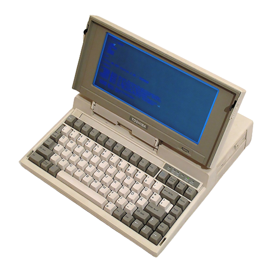
Toshiba Personal Computer T1200 (hereinafter referred to as T1200) is a
portable personal computer which is compatible with IBM PC situated at
higher rank of portable computer than Toshiba T1100 PLUS. It provides
many powerful functions in spite of its compact size and internal
battery pack which is removal. Hardware of the T1200, most of IC chips
are C-MOS type so that the power consumption is very little and Gate
Array chips are applied so that it is very compact and light weight.
The T1200 is composed of as follows:
System PCB (Printed
3.5-inch floppy disk drive
3.5-inch hard disk drive
LCD (Liquid crystal display)
Keyboard
Intelligent power supply PCB
Built-in modem
FIGURE 1-1 T1200 Personal Computer
Page 1-2
A 3.5-inch Floppy disk drive (FDD) is double-sided, double-density,
double-track with storage capacity of 720 kilobytes (formatted). A
3.5-inch hard disk drive (HDD) with storage capacity of 20 megabytes is
an equipment of the former. The high-resolution liquid crystal display
(LCD) with pixels of 640 in columns and 200 in rows.
The keyboard has 82 keys. For most applications it can be used exactly
like a standard typewriter keyboard.
Intelligent power supply apart from those ordinary power serving
functions, this unit contains a so-called "one-chip microcomputer", and
it controls the whole system PCB, FDD, HDD and HDC.
The built-in modem expands the capabilities of your system. The
built-in modem enables the system to communicate with an asynchronous
communications device through a telephone line. The modem can operate
communications at either low (300
The T1200 provided connecting to the optional devices at the rear panel
of the system. There are six connectors such as a parallel printer, an
RGB direct drive CRT display, an external FDD, an external key pad and
an RS-232C device.
MODEL:T1200H/HB
Page 1-3
1.2 SYSTEM PCB
curcuit board)
bps) or high (1200
bps) speed.
Advertisement

Related Manuals for Toshiba T1200


Summary of Contents for Toshiba T1200
- Page 1 Toshiba T1100 PLUS. It provides many powerful functions in spite of its compact size and internal battery pack which is removal. Hardware of the T1200, most of IC chips are C-MOS type so that the power consumption is very little and Gate Array chips are applied so that it is very compact and light weight.
- Page 2 System PCB is composed of the following devices: Central processor: CPU (80C86-2) (9.54 MHz/4.77 MHz) Numeric data processor: NPU (8087, optional) Memory System memory kbytes Expanded memory ... kbytes BIOS ROM kbytes Video RAM kbytes System support elements Direct memory access: DMA (82C37) Timer : (82C53) Programmable interrupt controller: PIC (82C59) Floppy disk controller: FDC (8565)
- Page 3 ³ ³ ³ F/H type ³ ÃÄÄÄÄÄÄÄÅÄÄÄÄÄÄÄÄÄÄÄÄÄÄÄÄÄÄÅÄÄÄÄÄÄÄÄÄÄÄÄÄÄÄÄÄÄÄÄÄÄÄÄÄÄÄÄÄÄÄÄÄÄÄÄÄÄÄÄÄÄÄÄ ÄÄÄÄÄÄÄ´ ³ ³ PJ18 ³ ³ ³ ³ ÚÄÄÄÄÄÄÄ¿ ³ ³ ³ ³ ³ 1 2 ³ 3 ³ Normal ³ ³ PJ18 ³ ÀÄÄÄÄÄÄÄÙ ³ ³ ³ PJ19 ³ PJ19 1 ³ ³...
- Page 4 Page 1-6 1.3 3.5-INCH FLOPPY DISK DRIVE The floppy disk drive (FDD) used in the T1200 is high performance, high reliable, slim sized FDD for 3.5-inch floppy disks with recording capacity of 1 Mbyte (unformatted) in double-sided, double density and 135 tracks per inch operation.
- Page 5 The hard disk drive (HDD) is random access storage, having recording capacity of 20 Mbytes. This is equipped with the storage media of non-removable 3.5-inch magnetic disks and mini- winchester type magnetic heads. The specifications are as following table. FIGURE 1-4 3.5-inch Hard Disk Drive TABLE 1-3 3.5-inch Hard Disk Drive Specifications ÚÄÄÄÄÄÄÄÄÄÄÄÄÄÄÄÄÄÄÄÄÄÄÄÄÄÄÄÄÄÄÄÄÄÄÄÄÄÄÄÄÄÂÄÄÄÄÄÄÄÄÄÄÄÄÄÄÄÄÄÄÄÄÄÄÄÄÄÄÄÄÄ...
- Page 6 1.5 HARD DISK CONTROL PCB Hard disk control PCB (HDC) is accompanied by hard disk drive (HDD) and connects to the system PCB through a cable. This HDC can interface the HDD to the system PCB. The specifications are as following table. FIGURE 1-5 Hard Disk Control PCB TABLE 1-4 Hard Disk Control PCB Specifications ÚÄÄÄÄÄÄÄÄÄÄÄÄÄÄÄÄÄÄÄÄÄÄÄÄÄÄÄÄÄÄÄÄÄÄÄÄÄÄÄÄÄÄÄÄÄÄÄÄÄÂÄÄÄÄÄÄÄÄÄÄÄÄÄÄÄÄÄÄÄÄÄ...
- Page 7 FIGURE 1-6 Keyboard MODEL:T1200H/HB Page 1-10 1.7 LIQUID CRYSTAL DISPLAY The liquid crystal display (LCD) is a graphics type display unit which has a resolution of 640 in horizontal (or column) by 200 in vertical (or row) directions. This unit is composed of the display panel, power supply and driver circuits.
- Page 8 contains the following functions. Control and monitoring of the stored main battery. This performs recharge control, detection of the available capacity, and that of the low battery. 1. Monitoring of AC adapter 2. Monitoring of DC output voltage 3. Power on/off control of the system unit 4.
- Page 9 ³ ³ ³ ³ 10mA ³ ÃÄÄÄÄÄÄÄÄÄÄÄÄÄÄÄÄÄÄÄÄÄÄÄÄÄÄÄÄÄÄÄÄÄÄÄÄÄÅÄÄÄÄÄÄÄÄÄÄÄÄÅÄÄÄÄÄÄÄÄÄÄÄÄÄÄÄÄÅÄÄÄ ÄÄÄÄÄÄ´ ³ ³ ³ ³ 10mA ³ ÃÄÄÄÄÄÄÄÄÄÄÄÄÄÄÄÄÄÄÄÄÄÄÄÄÄÄÄÄÄÄÄÄÄÄÄÄÄÅÄÄÄÄÄÄÄÄÄÄÄÄÅÄÄÄÄÄÄÄÄÄÄÄÄÄÄÄÄÅÄÄÄ ÄÄÄÄÄÄ´ ³ RS-232C, BUILT IN MODEM OR I/O SLOT³ ³ ³ 30mA ³ ÀÄÄÄÄÄÄÄÄÄÄÄÄÄÄÄÄÄÄÄÄÄÄÄÄÄÄÄÄÄÄÄÄÄÄÄÄÄÁÄÄÄÄÄÄÄÄÄÄÄÄÁÄÄÄÄÄÄÄÄÄÄÄÄÄÄÄÄÁÄÄÄ ÄÄÄÄÄÄÙ MODEL:T1200H/HB Page 1-12 1.9 BUILT-IN MODEM The built-in modem is connected to the connector that is used exclusively for this system PCB.
- Page 10 Multimeter Printer port LED The problem isolation flowchart described in part 2.2 can be used to determine the necessary isolation procedures to be followed when there is a problem with the T1200. MODEL:T1200H/HB Page 2-1 2.2 PROBLEM ISOLATION FLOWCHART This flowchart is used as a guide for determining which FRU is defective.
- Page 11 No disk is in the FDD. The HDD switch is off. The ac adapter is disconnected. All optional equipment is disconnected. See next page. Page 2-2 FIGURE 2-1 Problem Isolation Flowchart Page 2-3 FIGURE 2-1 Problem Isolation Flowchart con't. If an error is generated on the system test, memory test, display test and real time test, go to system PCB isolation procedures in part 2.4.
- Page 12 Turn the POWER switch on. If the Low Battery indicator lights, plug the ac adapter into the DC IN 12V jack. If the indicator then goes out, the battery is normal and you should go to PROCEDURE 3; if it remains lit, go to PROCEDURE 2.
- Page 13 Turn the POWER switch off. Remove the power supply PCB. (Refer to part 4.8) Plug the ac adapter into an electrical outlet and the DC IN 12V jack. Turn the POWER switch on. Use a multimeter to confirm that the output voltages for the three power supply PCB connectors conform to the values given in the following table.
- Page 14 defective. The defective unit must be isolated and replaced. MODEL:T1200H/HB Page 2-10 2.4 SYSTEM PCB ISOLATION PROCEDURES This section describes how to determine whether the system PCB is defective or not. The procedures below are outlined in the following pages. They should be performed in the order indicated. PROCEDURE 1: Message Check PROCEDURE 2:...
- Page 15 Page 2-12 PROCEDURE 2 Printer Port LED Check Turn the POWER switch off. Plug the printer port LED into the PRT (printer) connector on the back of the unit. Turn the POWER switch on while watching the printer port LED. The printer port LED will light at the same time that the POWER switch is turned on.
- Page 16 Confirm that the jumper straps status is normal. (Refer to part 1.2.1.) If the jumper strap status is normal, go to PROCEDURE 4. If the jumper strap status is not normal, set them correctly. FIGURE 2-5 Jumper Straps Page 2-14 PROCEDURE 4 Test Program Execution Execute the following test program.
- Page 17 This section describes how to determine whether the floppy disk drive is defective or not. The procedures below are outlined in the following pages. They should be performed in the order indicated. PROCEDURE 1: Test and Diagnostic Program Loading Check PROCEDURE 2: Message Check PROCEDURE 3: Head Cleaning PROCEDURE 4: FDD Test Execution...
- Page 18 go to PROCEDURE 3. If neither of the above messages appears, go to PROCEDURE 5. Page 2-19 PROCEDURE 3 Head Cleaning Turn the POWER switch off. Insert the cleaning disk to the FDD. Turn the POWER switch on, then will clean the head of the FDD. Remove the cleaning disk from the FDD.
- Page 19 ÃÄÄÄÄÄÄÄÄÄÅÄÄÄÄÄÄÄÄÄÄÄÄÄÄÄÄÄÄÄÄÄÄÄÄÄÄÄÄÄÄÄÄÄÄÄÄÄÄ´ ³ ³ SEEK ERROR ³ ÃÄÄÄÄÄÄÄÄÄÅÄÄÄÄÄÄÄÄÄÄÄÄÄÄÄÄÄÄÄÄÄÄÄÄÄÄÄÄÄÄÄÄÄÄÄÄÄÄ´ ³ ³ FDD not drive ³ ÃÄÄÄÄÄÄÄÄÄÅÄÄÄÄÄÄÄÄÄÄÄÄÄÄÄÄÄÄÄÄÄÄÄÄÄÄÄÄÄÄÄÄÄÄÄÄÄÄ´ ³ ³ Time Out Error (Not Ready) ³ ÃÄÄÄÄÄÄÄÄÄÅÄÄÄÄÄÄÄÄÄÄÄÄÄÄÄÄÄÄÄÄÄÄÄÄÄÄÄÄÄÄÄÄÄÄÄÄÄÄ´ ³ ³ Write buffer error ³ ÀÄÄÄÄÄÄÄÄÄÁÄÄÄÄÄÄÄÄÄÄÄÄÄÄÄÄÄÄÄÄÄÄÄÄÄÄÄÄÄÄÄÄÄÄÄÄÄÄÙ Page 2-21 PROCEDURE 5 FDD Connector Check Turn the POWER switch off and disconnect the ac adapter from the DC IN 12V jack.
- Page 20 This section describes how to determine whether the Hard Disk Drive is defective or not. The procedures below are outlined in the following pages. They should be performed in the order indicated. PROCEDURE 1: HDD Indicator Check PROCEDURE 2: Format Execution PROCEDURE 3: Hard Disk Test Execution PROCEDURE 4: Connector Check PROCEDURE 5: Jumper Strap Check...
- Page 21 Page 2-26 PROCEDURE 3 Hard Disk Drive Test Execution CAUTION: The contents of the hard disk will be erased when the test program is run. Before running the test, transfer the contents of the hard disk on the floppy disk. This can be done with the MS-DOS BACKUP command.
- Page 22 ÃÄÄÄÄÄÄÄÄÄÅÄÄÄÄÄÄÄÄÄÄÄÄÄÄÄÄÄÄÄÄÄÄÄÄÄÄÄÄÄÄÄÄÄÄÄÄÄÄ´ ³ ³ Write fault ³ ÃÄÄÄÄÄÄÄÄÄÅÄÄÄÄÄÄÄÄÄÄÄÄÄÄÄÄÄÄÄÄÄÄÄÄÄÄÄÄÄÄÄÄÄÄÄÄÄÄ´ ³ ³ Status error ³ ÃÄÄÄÄÄÄÄÄÄÅÄÄÄÄÄÄÄÄÄÄÄÄÄÄÄÄÄÄÄÄÄÄÄÄÄÄÄÄÄÄÄÄÄÄÄÄÄÄ´ ³ ³ Not sense error ( HW.code = FF) ³ ÀÄÄÄÄÄÄÄÄÄÁÄÄÄÄÄÄÄÄÄÄÄÄÄÄÄÄÄÄÄÄÄÄÄÄÄÄÄÄÄÄÄÄÄÄÄÄÄÄÙ Page 2-27 PROCEDURE 4 Connector Check Turn the POWER switch off. Disconnect the ac adapter from the DC IN 12V jack. Remove the top cover assembly.
- Page 23 Replace the HDC. (Refer to part 4.11.) Connect the new HDC to the system PCB and HDD, then other connectors too. If normal operation is restored, the previous HDC was defective. Assemble the system. If normal operation is not restored, HDD is probably defective. Go to PROCEDURE 7.
- Page 24 (any character or the space bar). If the character you hit appears on the screen, go to PROCEDURE 2. If the character does not appear, go to PROCEDURE 3. ÚÄÄÄÄÄÄÄÄÄÄÄÄÄÄÄÄÄÄÄÄÄÄÄÄÄÄÄÄÄÄÄÄÄÄÄÄÄÄÄÄÄÄÄÄÄÄÄÄÄÄÄÄÄÄÄÄ¿ ³ Toshiba Personal Computer MS-DOS Version 3.20/(RXXXXX) ³ ³ ³ ³...
- Page 25 PROCEDURE 4 New Keyboard Connection Turn the POWER switch off and disconnect the ac adapter from the DC IN 12V jack. Remove the keyboard unit. (Refer to part 4.4.) Connect the new keyboard to the system PCB. If normal operation is restored after connect the keyboard, the previous keyboard was defective.
- Page 26 If the message appears, go to PROCEDURE 3. If the message does not appear, first do the following: Confirm that the contrast knob is adjusted correctly. Confirm that the display is not on an external CRT. (The CRT indicator lamp will be lit if the display is on an external CRT.) After confirming (a) and (b) above, perform steps 1 and 2 again.
- Page 27 If it is not connected securely, reconnect it. FIGURE 2-13 System PCB Connector Check Page 2-41 PROCEDURE 5 LCD Module Connector Check Turn the POWER switch off and disconnect the ac adapter from the DC IN 12V jack. Take out the LCD module (Refer to part 4.15.) and confirm that the LCD cable is connected securely to the module.
- Page 28 This part explains test and diagnostic programs. The purpose of the test and diagnostic programs is to check the functions of all hardware modules of the T1200 Personal Computer. There are 17 programs; they are composed of two modules: the service program module (DIAGNOSTICS MENU) and test program module (DIAGNOSTIC TEST MENU).
- Page 29 ÚÄÄÄÄÄÄÄÄÄÄÄÄÄÄÄÄÄÄÄÄÄÄÄÄÄÄÄÄÄÄÄÄÄÄÄÄÄÄÄÄÄÄÄÄÄÄÄÄÄÄ¿ ³ TOSHIBA personal computer T1200 DIAGNOSTICS ³ ³ Version 1.00 (C) copyright TOSHIBA Corp. 1987 ³ ³ ³ ³ DIAGNOSTIC MENU ³ ³ ³ ³ 1 - DIAGNOSTIC TEST ³ ³ 2 - HARD DISK FORMAT ³ ³ ³...
- Page 30 When select the FLOPPY DISK TEST, the following messages will appear. Test drive number select (1:FDD1,2:FDD2,0:FDD1&2)? Media in drive#1 mode (1:360k,2:360k-1.2M/720k,3:1.2M,4:720k)? When select the HARD DISK TEST, the following message will appear. Test drive number select (1:HDD1,2:HDD2,0:HDD1&2)? After pressing the test number (1 to 11) of the DIAGNOSTIC TEST MENU, the following display (sample) will appear.
- Page 31 When select the (NO); When an error occurs, it displays the error status then it increments the error counter by one and goes to the next test. Type the 1 or 2 then press the Enter. The test program will run. Each subtest names described in the part 3.3.
- Page 32 ³ ³ ³ ³ Character attributes ³ ³ ³ ³ ³ Character set ³ ³ ³ ³ ³ 80*25 Character display ³ ³ 4 ³ DISPLAY ³ ³ 320*200 Graphics display ³ ³ ³ ³ ³ 640*200 Graphics display ³ ³...
- Page 33 PCB. (Test extent : F0000H - FFFFFH 64KB) Subtest 02 HDD off-SW Note: Confirm that turn the HDD switch on. After checking the operation of the HDD switch, confirm that signals are being exchange between the CPU and the PS (Power Supply). Operation for the test is as follows.
- Page 34 can not be carried out here. Subtest 05 Backup RAM (Execution time: 1 second) This test writes data (FFH, AAH, 55H, 00H) to the memory address (F0000H to F07FFH); then read it the data out and compares it to the original data. Page 3-8 Subtest 06 EMS function (Execution time: 16 seconds;...
- Page 35 changed to the character "*" only when it is pressed, and if released, it gets back to the original state. Ctrl key, Shift key, Alt key KEYBOARD TEST IN PROGRESS 30100 Page 3-10 Subtest 02 Tenkey pad display Note: This test can be executed only when the Tenkey pad is connected to the key pad connector.
- Page 36 ³ ³ ³ ³ ÃÄÄÄÄÄÄÄÄÄÄÅÄÄÄÄÄÄÄÄÄÄÄÄÄÄÄÄÅÄÄÄÄÄÄÄÄÄÄÄÄÄÄÄÄÄ´ ³ ³ ³ ³ ÃÄÄÄÄÄÄÄÄÄÄÅÄÄÄÄÄÄÄÄÄÄÄÄÄÄÄÄÅÄÄÄÄÄÄÄÄÄÄÄÄÄÄÄÄÄ´ ³ ³ ³ ³ ÃÄÄÄÄÄÄÄÄÄÄÅÄÄÄÄÄÄÄÄÄÄÄÄÄÄÄÄÅÄÄÄÄÄÄÄÄÄÄÄÄÄÄÄÄÄ´ ³ ³ ³ ³ ÃÄÄÄÄÄÄÄÄÄÄÅÄÄÄÄÄÄÄÄÄÄÄÄÄÄÄÄÅÄÄÄÄÄÄÄÄÄÄÄÄÄÄÄÄÄ´ ³ ³ ³ ³ ÃÄÄÄÄÄÄÄÄÄÄÅÄÄÄÄÄÄÄÄÄÄÄÄÄÄÄÄÅÄÄÄÄÄÄÄÄÄÄÄÄÄÄÄÄÄ´ ³ ³ ³ ³ ÃÄÄÄÄÄÄÄÄÄÄÅÄÄÄÄÄÄÄÄÄÄÄÄÄÄÄÄÅÄÄÄÄÄÄÄÄÄÄÄÄÄÄÄÄÄ´ ³ ³ ³ ³ ÃÄÄÄÄÄÄÄÄÄÄÅÄÄÄÄÄÄÄÄÄÄÄÄÄÄÄÄÅÄÄÄÄÄÄÄÄÄÄÄÄÄÄÄÄÄ´ ³ ³ ³ ³ ÃÄÄÄÄÄÄÄÄÄÄÅÄÄÄÄÄÄÄÄÄÄÄÄÄÄÄÄÅÄÄÄÄÄÄÄÄÄÄÄÄÄÄÄÄÄ´ ³...
- Page 37 ³ ³ ³ ³ ÃÄÄÄÄÄÄÄÄÄÄÅÄÄÄÄÄÄÄÄÄÄÄÄÄÄÄÄÅÄÄÄÄÄÄÄÄÄÄÄÄÄÄÄÄÄ´ ³ ³ ³ ³ ÃÄÄÄÄÄÄÄÄÄÄÅÄÄÄÄÄÄÄÄÄÄÄÄÄÄÄÄÅÄÄÄÄÄÄÄÄÄÄÄÄÄÄÄÄÄ´ ³ ³ ³ ³ ÃÄÄÄÄÄÄÄÄÄÄÅÄÄÄÄÄÄÄÄÄÄÄÄÄÄÄÄÅÄÄÄÄÄÄÄÄÄÄÄÄÄÄÄÄÄ´ ³ ³ ³ ³ ÃÄÄÄÄÄÄÄÄÄÄÅÄÄÄÄÄÄÄÄÄÄÄÄÄÄÄÄÅÄÄÄÄÄÄÄÄÄÄÄÄÄÄÄÄÄ´ ³ ³ ³ ³ ÃÄÄÄÄÄÄÄÄÄÄÅÄÄÄÄÄÄÄÄÄÄÄÄÄÄÄÄÅÄÄÄÄÄÄÄÄÄÄÄÄÄÄÄÄÄ´ ³ ³ ³ ³ ÀÄÄÄÄÄÄÄÄÄÄÁÄÄÄÄÄÄÄÄÄÄÄÄÄÄÄÄÁÄÄÄÄÄÄÄÄÄÄÄÄÄÄÄÄÄÙ <fig id=MMS\1200\12003_12.TIF>Page 3-12 TABLE 3-2 Scan Code, Character Code, and Key Top Name ÚÄÄÄÄÄÄÄÄÄÄÂÄÄÄÄÄÄÄÄÄÄÄÄÄÄÄÄÂÄÄÄÄÄÄÄÄÄÄÄÄÄÄÄÄÄ¿...
- Page 38 ÃÄÄÄÄÄÄÄÄÄÄÅÄÄÄÄÄÄÄÄÄÄÄÄÄÄÄÄÅÄÄÄÄÄÄÄÄÄÄÄÄÄÄÄÄÄ´ ³ ³ ³ ³ ÃÄÄÄÄÄÄÄÄÄÄÅÄÄÄÄÄÄÄÄÄÄÄÄÄÄÄÄÅÄÄÄÄÄÄÄÄÄÄÄÄÄÄÄÄÄ´ ³ ³ ³ ³ ÃÄÄÄÄÄÄÄÄÄÄÅÄÄÄÄÄÄÄÄÄÄÄÄÄÄÄÄÅÄÄÄÄÄÄÄÄÄÄÄÄÄÄÄÄÄ´ ³ ³ ³ ³ ÃÄÄÄÄÄÄÄÄÄÄÅÄÄÄÄÄÄÄÄÄÄÄÄÄÄÄÄÅÄÄÄÄÄÄÄÄÄÄÄÄÄÄÄÄÄ´ ³ Home ³ ³ ³ ÃÄÄÄÄÄÄÄÄÄÄÅÄÄÄÄÄÄÄÄÄÄÄÄÄÄÄÄÅÄÄÄÄÄÄÄÄÄÄÄÄÄÄÄÄÄ´ ³ ³ ³ ³ ÃÄÄÄÄÄÄÄÄÄÄÅÄÄÄÄÄÄÄÄÄÄÄÄÄÄÄÄÅÄÄÄÄÄÄÄÄÄÄÄÄÄÄÄÄÄ´ ³ Pg Dn ³ ³ ³ ÃÄÄÄÄÄÄÄÄÄÄÅÄÄÄÄÄÄÄÄÄÄÄÄÄÄÄÄÅÄÄÄÄÄÄÄÄÄÄÄÄÄÄÄÄÄ´ ³ ³ ³ ³ ÃÄÄÄÄÄÄÄÄÄÄÅÄÄÄÄÄÄÄÄÄÄÄÄÄÄÄÄÅÄÄÄÄÄÄÄÄÄÄÄÄÄÄÄÄÄ´ ³ Sys Req ³...
- Page 39 Subtest Character set (Execution time: 1 second) In this test the character code (00H to FFH) characters are displayed in the 40 x 25 pixel mode as shown below. CHARACTER SET IN 40X25 Subtest 04 80*25 Character display (Execution time: 1 second) In this test the shift characters are displayed in the 80 x 25 pixel mode as shown below.
- Page 40 shown below. ÚÄÄÄÄÄÄÄÄÄÄÄÄÄÄÄÄÄÄÄÄÄÄÄÄÄÄÄÄÄÄÄÄÄÄÄÄÄÄÄÄÄÄÄÄÄÄÄÄÄÄÄÄÄÄÄ¿ ³HHHHHHHHHHHHHHHHHHHHHHHHHHHHHHHHHHHHHHHHHHHHHHHHHHHHHHH³ ³HHHHHHHHHHHHHHHHHHHHHHHHHHHHHHHHHHHHHHHHHHHHHHHHHHHHHHH³ ³HHHHHHHHHHHHHHHHHHHHHHHHHHHHHHHHHHHHHHHHHHHHHHHHHHHHHHH³ ³HHHHHHHHHHHHHHHHHHHHHHHHHHHHHHHHHHHHHHHHHHHHHHHHHHHHHHH³ ³HHHHHHHHHHHHHHHHHHHHHHHHHHHHHHHHHHHHHHHHHHHHHHHHHHHHHHH³ ³HHHHHHHHHHHHHHHHHHHHHHHHHHHHHHHHHHHHHHHHHHHHHHHHHHHHHHH³ ³HHHHHHHHHHHHHHHHHHHHHHHHHHHHHHHHHHHHHHHHHHHHHHHHHHHHHHH³ ³HHHHHHHHHHHHHHHHHHHHHHHHHHHHHHHHHHHHHHHHHHHHHHHHHHHHHHH³ ³HHHHHHHHHHHHHHHHHHHHHHHHHHHHHHHHHHHHHHHHHHHHHHHHHHHHHHH³ ³HHHHHHHHHHHHHHHHHHHHHHHHHHHHHHHHHHHHHHHHHHHHHHHHHHHHHHH³ ³HHHHHHHHHHHHHHHHHHHHHHHHHHHHHHHHHHHHHHHHHHHHHHHHHHHHHHH³ ³HHHHHHHHHHHHHHHHHHHHHHHHHHHHHHHHHHHHHHHHHHHHHHHHHHHHHHH³ ³HHHHHHHHHHHHHHHHHHHHHHHHHHHHHHHHHHHHHHHHHHHHHHHHHHHHHHH³ ³HHHHHHHHHHHHHHHHHHHHHHHHHHHHHHHHHHHHHHHHHHHHHHHHHHHHHHH³ ³HHHHHHHHHHHHHHHHHHHHHHHHHHHHHHHHHHHHHHHHHHHHHHHHHHHHHHH³ ÀÄÄÄÄÄÄÄÄÄÄÄÄÄÄÄÄÄÄÄÄÄÄÄÄÄÄÄÄÄÄÄÄÄÄÄÄÄÄÄÄÄÄÄÄÄÄÄÄÄÄÄÄÄÄÄÙ Page 3-17 Subtest 09 Special attribute test This test executes the following test. 1. EXT/FDD SW test 2. CRT, Speed, Caps, Num, Scroll LED test 3.
- Page 41 Page 3-18 3. After pressing the Enter, the following message will appear. ÚÄÄÄÄÄÄÄÄÄÄÄÄÄÄÄÄÄÄÄÄÄÄÄÄÄÄÄÄÄÄÄÄÄÄÄÄÄÄÄÄÄÄÄÄÄÄÄÄÄÄÄÄÄÄ¿ ³ [ Speed/CRT LCD test ] ³ ³ ³ ³ (1) Press [ Fn + Pgdn I key ! ... Speed (red) ³ ³ (2) Press [ Fn + Pgup ] key ! ...
- Page 42 Track 0 to 79 Subtest 02 Sequential read/write (Execution time: 130 seconds) This test writes data to all tracks (as defined above) continuously and then reads the data out and compares it to original data. (The data pattern is B5ADADH repeated.) Subtest 03 Random address/data (Execution time: 12 seconds) This test writes random data to random address on all...
- Page 43 Subtest 03 Wrap around (Execution time: 1 second) Note: A printer wraparound connector is necessary for executing this test. Wiring diagram of the printer wrap around connector described in the part 3.22. Checks the data, control, and status lines with the printer wrap around connector.
- Page 44 Page 3-22 Subtest 05 Card modem loopback (Execution time: 5 seconds) Note: If there is no modem card in the system, this test can not be executed. Press the Fn + SysReq key, then confirm that the Built-in modem power is on. This test is used to check whether the data, which is from the modem to the RS232C inside the system, is same as the original data which had first been sent to the...
- Page 45 This test performs forward reading of contents from track 0 to track 610 and then performs reverse reading of the contents from track 610 to track 0. Subtest 02 Address uniquence (Execution time: 10 minutes) This test writes the address data(sector by sector) track by track, then reads the data and compares it to the original data.
- Page 46 MODEL:T1200H/HB Page 3-25 3.12 REAL TIMER TEST Subtest 01 Real time A new data and time can be input during this test when the current data and time are displayed. Operations for the test is as follows. 1. After executing the test, the following message will appear.
- Page 47 Confirm that the jumper strap is removed on the system PCB (PJ 20). If there is no NDP mounted and is removed the jumper strap on the system PCB, system is hung up. Must be turn the POWER switch off. Subtest 01 NDP test (Execution time: 1 second) This test checks the control word, status word, bus, and...
- Page 48 ÃÄÄÄÄÄÄÄÄÄÄÄÄÄÅÄÄÄÄÄÄÄÄÄÄÅÄÄÄÄÄÄÄÄÄÄÄÄÄÄÄÄÄÄÄÄÄÄÄÄÄÄÄÄÄÄÄÄÄÄÄ´ ³ ³ ³ Compare error ³ ÃÄÄÄÄÄÄÄÄÄÄÄÄÄÅÄÄÄÄÄÄÄÄÄÄÅÄÄÄÄÄÄÄÄÄÄÄÄÄÄÄÄÄÄÄÄÄÄÄÄÄÄÄÄÄÄÄÄÄÄÄ´ ³ ³ ³ Bad Command ³ ³ ³ ³ Address Mark Not Found ³ ³ ³ ³ Write Protected ³ ³ ³ ³ Record Not Found ³ ³ ³ ³ Media removed on dual attach card³...
- Page 49 ³ ³ ³ Write fault ³ ³ ³ ³ Status error ³ ³ ³ ³ Not sense error ( HW.code = FF) ³ ÃÄÄÄÄÄÄÄÄÄÄÄÄÅÄÄÄÄÄÄÄÄÄÄÄÅÄÄÄÄÄÄÄÄÄÄÄÄÄÄÄÄÄÄÄÄÄÄÄÄÄÄÄÄÄÄÄÄÄÄÄ´ ³ ³ ³ No NDP ³ ³ ³ ³ Control word error ³ ³ ³ ³ Status word error ³...
- Page 50 Executes the formatting of a specified cylinder and track as a good track. 3. Bad track FORMAT (Execution time: 1 second) Executes the formatting of a specified cylinder and track as a bad track. 4. Bad track CHECK (Execution time: 1 and 1/2 minutes) Checks for bad tracks by performing a read operation for all tracks on the hard disk;...
- Page 51 ÀÄÄÄÄÄÄÄÄÄÄÄÄÄÄÄÄÄÄÄÄÄÄÄÄÄÄÄÄÄÄÄÄÄÄÄÄÄÄÄÄÄÄÄÄÄÄÄÄÄÄÄÄÄÄÄÄÄÄÄÙ Page 3-31 (4) After checking all cylinders of the hard disk, the following message will appear. If founds the bad track, displays the bad track number. Press [Bad track number (CCCH) key ? (5) If the hard disk has except the displayed the bad track number, type a bad-track number (four digits) and press Enter.
- Page 52 (5) After formatting the track of the hard disk, the Format complete message will appear. (6) Press the Enter to return to the HARD DISK FORMAT menu. Page 3-33 Bad track CHECK Selection (1) When Bad track CHECK is selected, the following message will appear.
- Page 53 After the above message appears, remove the Diagnostics disk, insert the cleaning disk, and press any key. When the following message appears, FDD head cleaning will begin. ÚÄÄÄÄÄÄÄÄÄÄÄÄÄÄÄÄÄÄÄÄÄÄÄÄÄÄÄÄÄÄÄÄÄÄÄÄÄÄÄÄÄÄÄÄÄÄÄÄÄÄÄÄÄÄÄÄÄÄÄ¿ ³ HEAD CLEANING ³ ³ ³ ³ Mount cleaning disk(s) on drive(s). ³...
- Page 54 The 1 key scrolls the display to the next page. The 2 key scrolls the display to the previous page. The 3 key returns the display to the DIAGNOSTIC MENU. The 4 key erases all error log information in RAM. The 5 key outputs error log information to a printer.
- Page 55 This program is repeated continuously. To stop the program, press Ctrl + Break key. MODEL:T1200H/HB Page 3-38 3.20 FDD UTILITIES 3.20.1 Program description These programs format and copy floppy disks, and display dump list for both the FDD and the HDD. FORMAT This program can format floppy disk (5.25"/3.5") as follows.
- Page 56 Page 3-39 FORMAT Selection (1) When FORMAT is selected, the following message appears. ÚÄÄÄÄÄÄÄÄÄÄÄÄÄÄÄÄÄÄÄÄÄÄÄÄÄÄÄÄÄÄÄÄÄÄÄÄÄÄÄÄÄÄÄÄÄÄÄÄÄÄÄÄÄÄÄÄÄÄÄ¿ ³ DIAGNOSTICS - FORMAT ³ ³ Drive number select (1:A, 2:B) ? _ ³ ÀÄÄÄÄÄÄÄÄÄÄÄÄÄÄÄÄÄÄÄÄÄÄÄÄÄÄÄÄÄÄÄÄÄÄÄÄÄÄÄÄÄÄÄÄÄÄÄÄÄÄÄÄÄÄÄÄÄÄÄÙ (2) Select a drive number. Type the number and the following message will then appear.
- Page 57 (3) Remove the diagnostics disk from the FDD and insert the source disk; press any key. The Copy started message will then appear. After that, the following message will appear. ÚÄÄÄÄÄÄÄÄÄÄÄÄÄÄÄÄÄÄÄÄÄÄÄÄÄÄÄÄÄÄÄÄÄÄÄÄÄÄÄÄÄÄÄÄÄÄÄÄÄÄÄÄÄÄÄÄÄÄÄ¿ ³ Insert target disk into drive A: ³ ³ Press any key when ready. ³...
- Page 58 (7) The Sector number ?? message will then appear. Type the sector number and press Enter. The dump list for the floppy disk will be displayed. (8) After a dump list appears on the screen, the Press number key (1:up,2:down,3:end) ? message will appear. 1.
- Page 59 ÀÄÄÄÄÄÄÄÄÄÄÄÄÄÄÄÄÄÄÄÄÄÄÄÄÄÄÄÄÄÄÄÄÄÄÄÄÄÄÄÄÄÄÄÄÄÄÄÄÄÄÙ Press Enter key to return to the DIAGNOSTICS MENU. MODEL:T1200H/HB Page 3-43 3.22 WIRING DIAGRAM 1. Printer wrap around connector (9) +DATA7(4)+DATA2 ÄÄÄÄ + SELECT (13) (8) +DATA6(3)+DATA1 ÄÄÄÄ + P.END (12) (7) +DATA5(2)+DATA0 ÄÄÄÄ + BUSY (11) (6) +DATA4(16)-INT PRT ÄÄÄÄ...
- Page 60 4. RS232C direct cable (9-pin to 25-pin) (1) CD ÄÄÄÄÄÄÄÄÄÄÄÄÄÄÄÄÄÄÄÄÄÄÄÄÄÄÄÄÄÄÄÄÄÄÄ> (2) RD (4) DTR ÄÄÄÄÄÄÄÄÄÄÄÄÄÄÄÄÄÄÄÄÂÄÄÄÄÄÄÄÄÄÄÄÄÄÄ> ³ ÃÄÄÄÄÄÄÄÄÄÄÄÄÄÄ> ³ ÀÄÄÄÄÄÄÄÄÄÄÄÄÄÄ> (22) (5) GND ÄÄÄÄÄÄÄÄÄÄÄÄÄÄÄÄÄÄÄÄÄÄÄÄÄÄÄÄÄÄÄÄÄÄÄÄ (7) RTS ÄÄÄÄÄÄÄÄÄÄÄÄÄÄÄÄÄÄÄÄÄÄÄÄÄÄÄÄÄÄÄÄÄÄÄ> (6) DSR <ÄÄÄÄÄÄÄÄÄÄÄÄÄÄÂÄÄÄÄÄÄÄÄÄÄÄÄÄÄÄÄÄÄÄ (20) ³ (8) CTS <ÄÄÄÄÄÄÄÄÄÄÄÄÄÄ´ ³ (9) RI <ÄÄÄÄÄÄÄÄÄÄÄÄÄÄÙ <fig id=MMS\1200\12003_44.TIF>FIGURE 3-4 RS232C Direct Cable (9-pin to 25-pin) MODEL:T1200H/HB Page 4-1...
- Page 61 The following points must be kept in mind: The system should never be disassembled unless there is a problem (abnormal operation, etc.). Only approved tools may be used. After deciding the purpose of replacing the unit, and the procedures required, do not carry out any other procedures which are not absolutely necessary.
- Page 62 FIGURE 4-4 Removing the Screws from the Top Cover Assembly Page 4-4 Open the LCD by sliding the two side latches (J) forward while pulling the LCD upward. FIGURE 4-5 Opening the LCD The top cover assembly can now be lifted and separated from the base subassembly.
- Page 63 bridge (A). Release the pressure plate (B) of connector PJ1 (C) to disconnect the keyboard cable from the system PCB. FIGURE 4-8 Disconnecting the Keyboard Unit To install a new keyboard unit, follow the above procedures in reverse. MODEL:T1200H/HB Page 4-7 4.5 REMOVING/REPLACING THE MEMORY CARD, RTC BATTERY, AND SPEAKER CAUTION: The expanded memory contents will remain in the old expanded memory.
- Page 64 Confirm that the POWER switch is off. Remove and disconnect the top cover assembly and lift out the keyboard unit as directed in parts 4.2 and 4.3. It is not necessary to disconnect the keyboard cable. Disconnect the two cables (A) and (B) from the system PCB (C). Lift up the keyboard bridge (D) and disconnect the LED cable (E) from the system PCB.
- Page 65 Page 4-10 4.8 REMOVING/REPLACING THE POWER SUPPLY PCB Confirm that the POWER switch is off. Remove the top cover assembly as directed in part 4.2. Disconnect the two forward cables (A) from the system PCB. DO NOT disconnect them from the power supply PCB (B). Disconnect the remaining three cables (C) from the power supply PCB.
- Page 66 Page 4-13 Remove the three screws (H) from the FDD base. After disconnecting the FDD cable (I) from the system PCB, gently lift the FDD base up and toward the front of the unit. At this time, remove the HDD mask panel (J) from the FDD base. To remove the expansion bus cable (K), remove the two screws (L) from the FDD base.
- Page 67 To remove the hard disk control PCB from the hard disk drive (D), disconnect the hard disk drive connector (E). FIGURE 4-17 Removing the Hard Disk Control PCB To install a new hard disk control PCB, follow the above procedures in reverse.
- Page 68 Open the LCD by sliding the two side latches (A) forward while pulling upward. FIGURE 4-21 Opening the LCD Page 4-20 Using tweezers or a fine-pointed instrument, peel off the TOSHIBA label (B) and keep it in a clean place. Remove the single flatheaded countersunk screw (C) and take the LCD mask (D) off by pulling it slightly forward and upward.
- Page 69 Confirm that the POWER switch is off. Remove the LCD mask from the LCD cover subassembly as directed in part 4.14. Remove the four screws (A) on the LCD module (B). FIGURE 4-23 Removing the LCD Screws Disconnect the LCD cable (C) from the LCD module. FIGURE 4-24 Removing and Disconnecting the LCD Module To install a new LCD module, follow the above procedures in reverse.
- Page 70 4.17 REPLACING THE LCD COVER SUBASSEMBLY Confirm that the POWER switch is off. Insert the torsion bar (A) into the hole (B) provided in the top cover. Make sure that the torsion bar is fully seated before proceeding; the hooked portion should be positioned vertically. FIGURE 4-28 Inserting the Torsion Bar Insert the short end of the hinge cover plastic cable shield (C) into the main unit;...
- Page 71 (E) Power supply PCB (L) Memory card (F) Sub battery (M) RTC battery (G) 3.5-inch floppy disk drive (N) Speaker (O) Base subassembly FIGURE 5-1 Inside the System Unit Page 5-2 5.1.2 Rear panel (A) RGB connector (9-pin D-shell) (B) COMP connector (2-pin) (C) Printer connector (25-pin D-shell) (D) Line jack (for built-in modem) (E) Battery pack...
- Page 72 Page 5-4 5.2 SYSTEM PCB 5.2.1 System PCB connectors FIGURE 5-4 System PCB Connectors Page 5-5 (A) PJ 1 Keyboard connector (B) PJ 2 System memory connector (C) PJ 3 System memory connector (D) PJ 4 HDC connector (E) PJ 5 RTC battery connector (F) PJ 6 Speaker connector (G) PJ 7 LED connector (H) PJ 8 Modem connector...
- Page 73 (A) CPU: Central processor (80C86A-2) (B) NDP socket (C) BIOS ROM (D) Gate Array (Display controller) (E) Gate Array (PRT/FDC) (F) Gate Array (Bus driver) (G) Gate Array (Bus controller) (H) Gate Array (EXP-MEM controller) (I) FDC: Floppy disk controller (TC8565) (J) ACE: Asynchronous communication element (TC8570) (K) PIC: Programmable interrupt controller (82C59A) (L) TIMER (82C54A)
- Page 74 ÃÄÄÄÄÄÄÄÄÄÅÄÄÄÄÄÄÄÄÄÅÄÄÄÄÄÄÄÅÄÄÄÄÄÄÄÄÄÄÄÄÄÄÄÄÄÄÄÄÄÄÄÄÄÄÄÄÄ´ ³ ³ PD51 ³ ³ +DATA BIT 5 ³ ÃÄÄÄÄÄÄÄÄÄÅÄÄÄÄÄÄÄÄÄÅÄÄÄÄÄÄÄÅÄÄÄÄÄÄÄÄÄÄÄÄÄÄÄÄÄÄÄÄÄÄÄÄÄÄÄÄÄ´ ³ ³ PD61 ³ ³ +DATA BIT 6 ³ ÃÄÄÄÄÄÄÄÄÄÅÄÄÄÄÄÄÄÄÄÅÄÄÄÄÄÄÄÅÄÄÄÄÄÄÄÄÄÄÄÄÄÄÄÄÄÄÄÄÄÄÄÄÄÄÄÄÄ´ ³ ³ PD71 ³ ³ +DATA BIT 7 ³ ÃÄÄÄÄÄÄÄÄÄÅÄÄÄÄÄÄÄÄÄÅÄÄÄÄÄÄÄÅÄÄÄÄÄÄÄÄÄÄÄÄÄÄÄÄÄÄÄÄÄÄÄÄÄÄÄÄÄ´ ³ ³ ACK0 ³ ³ -ACKNOWLEDGE ³ ÃÄÄÄÄÄÄÄÄÄÅÄÄÄÄÄÄÄÄÄÅÄÄÄÄÄÄÄÅÄÄÄÄÄÄÄÄÄÄÄÄÄÄÄÄÄÄÄÄÄÄÄÄÄÄÄÄÄ´ ³ ³...
- Page 75 ÃÄÄÄÄÄÅÄÄÄÄÄÄÄÄÄÄÄÅÄÄÄÄÄÄÄÅÄÄÄÄÄÄÄÄÄÄÄÄÄÄÄÄÄÄÄÄÄÄÄÄÄÄÄÄÄÄ´ ³ 15 ³ FSIDE0 ³ ³ -SIDE SELECT ³ ÃÄÄÄÄÄÅÄÄÄÄÄÄÄÄÄÄÄÅÄÄÄÄÄÄÄÅÄÄÄÄÄÄÄÄÄÄÄÄÄÄÄÄÄÄÄÄÄÄÄÄÄÄÄÄÄÄ´ ³ 16 ³ FDIRC0 ³ ³ -DIRECTION ³ ÃÄÄÄÄÄÅÄÄÄÄÄÄÄÄÄÄÄÅÄÄÄÄÄÄÄÅÄÄÄÄÄÄÄÄÄÄÄÄÄÄÄÄÄÄÄÄÄÄÄÄÄÄÄÄÄÄ´ ³ 17 ³ STEP0 ³ ³ -STEP ³ ÃÄÄÄÄÄÅÄÄÄÄÄÄÄÄÄÄÄÅÄÄÄÄÄÄÄÅÄÄÄÄÄÄÄÄÄÄÄÄÄÄÄÄÄÄÄÄÄÄÄÄÄÄÄÄÄÄ´ ³18-25³ ³ ³ GROUND (0 V) ³ ÀÄÄÄÄÄÁÄÄÄÄÄÄÄÄÄÄÄÁÄÄÄÄÄÄÄÁÄÄÄÄÄÄÄÄÄÄÄÄÄÄÄÄÄÄÄÄÄÄÄÄÄÄÄÄÄÄÙ Note Pin Number 14 is not supported at present, but it will be supported in the near future.
- Page 76 ÃÄÄÄÄÄÄÅÄÄÄÄÄÄÄÄÄÅÄÄÄÄÄÄÄÅÄÄÄÄÄÄÄÄÄÄÄÄÄÄÄÄÄÄÄÄÄÄÄÄÄÄÄÄÄÄ´ ³ ³ DSR1 ³ ³ +DATA SET READY ³ ÃÄÄÄÄÄÄÅÄÄÄÄÄÄÄÄÄÅÄÄÄÄÄÄÄÅÄÄÄÄÄÄÄÄÄÄÄÄÄÄÄÄÄÄÄÄÄÄÄÄÄÄÄÄÄÄ´ ³ ³ RTS1 ³ ³ +REQUEST TO SEND ³ ÃÄÄÄÄÄÄÅÄÄÄÄÄÄÄÄÄÅÄÄÄÄÄÄÄÅÄÄÄÄÄÄÄÄÄÄÄÄÄÄÄÄÄÄÄÄÄÄÄÄÄÄÄÄÄÄ´ ³ ³ CTS1 ³ ³ +CLEAR TO SEND ³ ÃÄÄÄÄÄÄÅÄÄÄÄÄÄÄÄÄÅÄÄÄÄÄÄÄÅÄÄÄÄÄÄÄÄÄÄÄÄÄÄÄÄÄÄÄÄÄÄÄÄÄÄÄÄÄÄ´ ³ ³ ³ ³ +RING INDICATOR ³ ÀÄÄÄÄÄÄÁÄÄÄÄÄÄÄÄÄÁÄÄÄÄÄÄÄÁÄÄÄÄÄÄÄÄÄÄÄÄÄÄÄÄÄÄÄÄÄÄÄÄÄÄÄÄÄÄÙ Page 5-11 5.3.5 COMP connector FIGURE 5-10 COMP Connector TABLE 5-5 COMP Connector Signal Names...
- Page 77 ³ ³ ³ ³ ³ ³ ³ ³ DATA BUS ³ ÃÄÄÄÄÄÅÄÄÄÄÄÄÄÄÅÄÄÄÄÄÄÅÄÄÄÄÄÄÄÄÄÄÄÄÄÄÄÄÄÄÄÄÄÄÄÄÅÄÄÄÄÄÅÄÄÄÄÄÄÄÄÅÄÄÄÄÄÅÄÄÄ ÄÄÄÄÄÄÄÄÄÄÄÄÄÄÄÄÄij ³ ³ MVEE ³ ³ -9VDC ³ 33 ³ SYD11 ³ I/O ³ BIDIRECTIONAL 8-BIT ³ ³ ³ ³ ³ ³ ³ ³ ³ DATA BUS ³ ÃÄÄÄÄÄÅÄÄÄÄÄÄÄÄÅÄÄÄÄÄÄÅÄÄÄÄÄÄÄÄÄÄÄÄÄÄÄÄÄÄÄÄÄÄÄÄÅÄÄÄÄÄÅÄÄÄÄÄÄÄÄÅÄÄÄÄÄÅÄÄÄ...
- Page 78 ³ ³ ³ ³ ³ ³ ³ ³ COMMAND ³ ÃÄÄÄÄÄÅÄÄÄÄÄÄÄÄÅÄÄÄÄÄÄÅÄÄÄÄÄÄÄÄÄÄÄÄÄÄÄÄÄÄÄÄÄÄÄÄÅÄÄÄÄÄÅÄÄÄÄÄÄÄÄÅÄÄÄÄÄÅÄÄÄ ÄÄÄÄÄÄÄÄÄÄÄÄÄÄÄÄÄÄ´ ³ 13 ³ A031 ³ ³ LOWER 16-BIT ADDRESS ³ 43 ³ GND ³ ³ GROUND(0V) ³ ÃÄÄÄÄÄÅÄÄÄÄÄÄÄÄÅÄÄÄÄÄÄÅÄÄÄÄÄÄÄÄÄÄÄÄÄÄÄÄÄÄÄÄÄÄÄÄÅÄÄÄÄÄÅÄÄÄÄÄÄÄÄÅÄÄÄÄÄÅÄÄÄ ÄÄÄÄÄÄÄÄÄÄÄÄÄÄÄÄÄÄ´ ³ 14 ³ A041 ³ ³ LOWER 16-BIT ADDRESS ³...
- Page 79 ÃÄÄÄÄÄÅÄÄÄÄÄÄÄÄÅÄÄÄÄÄÄÅÄÄÄÄÄÄÄÄÄÄÄÄÄÄÄÄÄÄÄÄÄÄÄÄÅÄÄÄÄÄÅÄÄÄÄÄÄÄÄÅÄÄÄÄÄÅÄÄÄ ÄÄÄÄÄÄÄÄÄÄÄÄÄÄÄÄÄÄ´ ³ 26 ³ A151 ³ ³ LOWER 16-BIT ADDRESS ³ 56 ³ DACK30 ³ O ³ DMA ACKNOWLEDGE ³ ³ ³ ³ ³ ³ ³ ³ ³ SIGNAL ³ ÃÄÄÄÄÄÅÄÄÄÄÄÄÄÄÅÄÄÄÄÄÄÅÄÄÄÄÄÄÄÄÄÄÄÄÄÄÄÄÄÄÄÄÄÄÄÄÅÄÄÄÄÄÅÄÄÄÄÄÄÄÄÅÄÄÄÄÄÅÄÄÄ ÄÄÄÄÄÄÄÄÄÄÄÄÄÄÄÄÄÄ´ ³ 27 ³ ³ ³ GROUND(0V) ³ 57 ³...
- Page 80 ÃÄÄÄÄÄÅÄÄÄÄÄÄÄÄÅÄÄÄÄÄÄÅÄÄÄÄÄÄÄÄÄÄÄÄÄÄÄÄÄÄÄÅÄÄÄÄÄÅÄÄÄÄÄÄÄÄÅÄÄÄÄÄÅÄÄÄÄÄÄÄÄ ÄÄÄÄÄÄÄÄÄÄÄÄÄ´ ³ ³ ³ ³ NOT USED ³ 27 ³ - ³ ³ NOT USED ³ ÃÄÄÄÄÄÅÄÄÄÄÄÄÄÄÅÄÄÄÄÄÄÅÄÄÄÄÄÄÄÄÄÄÄÄÄÄÄÄÄÄÄÅÄÄÄÄÄÅÄÄÄÄÄÄÄÄÅÄÄÄÄÄÅÄÄÄÄÄÄÄÄ ÄÄÄÄÄÄÄÄÄÄÄÄÄ´ ³ ³ ³ ³ NOT USED ³ 28 ³ IOERR0 ³ I ³ I/O ERROR ³ ÃÄÄÄÄÄÅÄÄÄÄÄÄÄÄÅÄÄÄÄÄÄÅÄÄÄÄÄÄÄÄÄÄÄÄÄÄÄÄÄÄÄÅÄÄÄÄÄÅÄÄÄÄÄÄÄÄÅÄÄÄÄÄÅÄÄÄÄÄÄÄÄ ÄÄÄÄÄÄÄÄÄÄÄÄÄ´ ³ ³ ³ ³...
- Page 81 ÀÄÄÄÄÄÁÄÄÄÄÄÄÄÄÁÄÄÄÄÄÄÁÄÄÄÄÄÄÄÄÄÄÄÄÄÄÄÄÄÄÄÁÄÄÄÄÄÁÄÄÄÄÄÄÄÄÁÄÄÄÄÄÁÄÄÄÄÄÄÄÄ ÄÄÄÄÄÄÄÄÄÄÄÄÄÙ MODEL:T1200H/HB Page 5-14 5.4 KEYBOARD LAYOUT 5.4.1 USA version FIGURE 5-12 USA Version Page 5-15 5.4.2 England version FIGURE 5-13 England Version Page 5-16 5.4.3 German version FIGURE 5-14 German Version Page 5-17 5.4.4 France version FIGURE 5-15 France Version Page 5-18 5.4.5 Spain version FIGURE 5-16 Spain Version...
- Page 82 Page 5-22 5.4.9 Keycap number FIGURE 5-20 Keycap Number MODEL:T1200H/HB Page 5-23 5.5 DISPLAY CODE TABLE 5-9 Display Code MODEL:T1200H/HB Page A-1 A.1 GENERAL The Bus Controller Gate Array is a 2,000 gate flat package type chip with 100 lead pins. It contains the following functions. Signal name and meaning of each pin used in this chip are explained in this section together with its detailed definitions.
- Page 83 FIGURE A-2 Block Diagram MODEL:T1200H/HB Page A-3 A.3 PIN DESCRIPTION TABLE A-1 Pin Description ÚÄÄÄÄÄÂÄÄÄÄÄÂÄÄÄÄÄÄÄÄÄÄÄÂÄÄÄÄÄÄÄÄÄÄÄÄÄÄÄÄÄÄÄÄÄÄÄÄÄÄÄÄÄÄÄÄÄÄÄÄÄÄÄÄ¿ ³ Pin ³ I/O ³ SYMBOL ³ Signal name and Description ³ ÃÄÄÄÄÄÅÄÄÄÄÄÅÄÄÄÄÄÄÄÄÄÄÄÅÄÄÄÄÄÄÄÄÄÄÄÄÄÄÄÄÄÄÄÄÄÄÄÄÄÄÄÄÄÄÄÄÄÄÄÄÄÄÄÄ´ ³ ³ I/O ³ ³ IOD71 ³ ³ ³ ³ ³ Bidirectional data bus bit 7 ³...
- Page 84 ÀÄÄÄÄÄÁÄÄÄÄÄÁÄÄÄÄÄÄÄÄÄÄÄÁÄÄÄÄÄÄÄÄÄÄÄÄÄÄÄÄÄÄÄÄÄÄÄÄÄÄÄÄÄÄÄÄÄÄÄÄÄÄÄÄÙ Page A-4 ÚÄÄÄÄÄÂÄÄÄÄÄÄÂÄÄÄÄÄÄÄÄÄÄÂÄÄÄÄÄÄÄÄÄÄÄÄÄÄÄÄÄÄÄÄÄÄÄÄÄÄÄÄÄÄÄÄÄÄÄÄÄÄÄÄÄÄÄ¿ ³ Pin ³ I/O ³ SYMBOL ³ Signal name and Description ³ ÃÄÄÄÄÄÅÄÄÄÄÄÄÅÄÄÄÄÄÄÄÄÄÄÅÄÄÄÄÄÄÄÄÄÄÄÄÄÄÄÄÄÄÄÄÄÄÄÄÄÄÄÄÄÄÄÄÄÄÄÄÄÄÄÄÄÄÄ´ ³ 14 ³ I ³ DACKO ³ DACK00 ³ ³ ³ ³ ³ DMA acknowledge signal for channel 0 ³ ÃÄÄÄÄÄÅÄÄÄÄÄÄÅÄÄÄÄÄÄÄÄÄÄÅÄÄÄÄÄÄÄÄÄÄÄÄÄÄÄÄÄÄÄÄÄÄÄÄÄÄÄÄÄÄÄÄÄÄÄÄÄÄÄÄÄÄÄ´ ³ 15 ³ ³...
- Page 85 ³Pin ³ I/O ³ SYMBOL ³ Signal name and Description ³ ÃÄÄÄÄÅÄÄÄÄÄÅÄÄÄÄÄÄÄÄÄÄÄÅÄÄÄÄÄÄÄÄÄÄÄÄÄÄÄÄÄÄÄÄÄÄÄÄÄÄÄÄÄÄÄÄÄÄÄÄÄÄÄÄÄÄÄÄÄ´ ³ 28 ³ ³ ³ + 5V ³ ÃÄÄÄÄÅÄÄÄÄÄÅÄÄÄÄÄÄÄÄÄÄÄÅÄÄÄÄÄÄÄÄÄÄÄÄÄÄÄÄÄÄÄÄÄÄÄÄÄÄÄÄÄÄÄÄÄÄÄÄÄÄÄÄÄÄÄÄÄ´ ³ 29 ³ I ³ XIOW ³ XWOIR0 ³ ³ ³ ³ ³ I/O write command (Buffer) ³ ÃÄÄÄÄÅÄÄÄÄÄÅÄÄÄÄÄÄÄÄÄÄÄÅÄÄÄÄÄÄÄÄÄÄÄÄÄÄÄÄÄÄÄÄÄÄÄÄÄÄÄÄÄÄÄÄÄÄÄÄÄÄÄÄÄÄÄÄÄ´ ³...
- Page 86 ³ 37 ³ I ³ INT87 ³ INT871 ³ ³ ³ ³ ³ 8087 interactive ³ ÃÄÄÄÄÅÄÄÄÄÄÅÄÄÄÄÄÄÄÄÄÄÄÅÄÄÄÄÄÄÄÄÄÄÄÄÄÄÄÄÄÄÄÄÄÄÄÄÄÄÄÄÄÄÄÄÄÄÄÄÄÄÄÄÄÄÄÄÄ´ ³ 38 ³ I ³ KSCLK ³ KSCLK1 ³ ³ ³ ³ ³ Keyboard status clock ³ ÃÄÄÄÄÅÄÄÄÄÄÅÄÄÄÄÄÄÄÄÄÄÄÅÄÄÄÄÄÄÄÄÄÄÄÄÄÄÄÄÄÄÄÄÄÄÄÄÄÄÄÄÄÄÄÄÄÄÄÄÄÄÄÄÄÄÄÄÄ´ ³ 39 ³ I ³ KSDAT ³...
- Page 87 ³ 45 ³ O ³ FAST ³ FAST1 ³ ³ ³ ³ ³ CPU clock mode ("High" 9.54 MHz, ³ ³ ³ ³ ³ "low" = 4.77 MHz) ³ ÃÄÄÄÄÄÄÅÄÄÄÄÄÅÄÄÄÄÄÄÄÄÄÄÄÅÄÄÄÄÄÄÄÄÄÄÄÄÄÄÄÄÄÄÄÄÄÄÄÄÄÄÄÄÄÄÄÄÄÄÄÄÄÄÄÄÄÄÄÄÄ´ ³ 46 ³ I ³ TEST 1 ³ PO3A0 ³ ³...
- Page 88 ÀÄÄÄÄÄÄÁÄÄÄÄÄÁÄÄÄÄÄÄÄÄÄÄÄÁÄÄÄÄÄÄÄÄÄÄÄÄÄÄÄÄÄÄÄÄÄÄÄÄÄÄÄÄÄÄÄÄÄÄÄÄÄÄÄÄÄÄÄÄÄÙ Page A-7 ÚÄÄÄÄÄÂÄÄÄÄÄÂÄÄÄÄÄÄÄÄÄÄÄÂÄÄÄÄÄÄÄÄÄÄÄÄÄÄÄÄÄÄÄÄÄÄÄÄÄÄÄÄÄÄÄÄÄÄÄÄÄÄÄÄÄÄÄÄ¿ ³ Pin ³ I/O ³ SYMBOL ³ Signal name and Description ³ ÃÄÄÄÄÄÅÄÄÄÄÄÅÄÄÄÄÄÄÄÄÄÄÄÅÄÄÄÄÄÄÄÄÄÄÄÄÄÄÄÄÄÄÄÄÄÄÄÄÄÄÄÄÄÄÄÄÄÄÄÄÄÄÄÄÄÄÄÄ´ ³ 56 ³ ³ IOER ³ IOERR0 ³ ³ ³ ³ ³ I/O error. It is low active. ³ ÃÄÄÄÄÄÅÄÄÄÄÄÅÄÄÄÄÄÄÄÄÄÄÄÅÄÄÄÄÄÄÄÄÄÄÄÄÄÄÄÄÄÄÄÄÄÄÄÄÄÄÄÄÄÄÄÄÄÄÄÄÄÄÄÄÄÄÄÄ´ ³ 57 ³ ³...
- Page 89 ³ Pin³ I/O ³ SYMBOL ³ Signal name and Description ³ ÃÄÄÄÄÅÄÄÄÄÄÄÅÄÄÄÄÄÄÄÄÄÄÄÅÄÄÄÄÄÄÄÄÄÄÄÄÄÄÄÄÄÄÄÄÄÄÄÄÄÄÄÄÄÄÄÄÄÄÄÄÄÄÄÄÄÄÄÄ´ ³ 72³ ³ ³ DMAEN ³ ³ ³ ³ ³ DMA address enable signal. This ³ ³ ³ ³ ³ signal is generated ³ ³ ³ ³ ³ from the AEN signal of the 82C37 ³...
- Page 90 ÃÄÄÄÄÅÄÄÄÄÅÄÄÄÄÄÄÅÄÄÄÄÄÄÄÄÄÄÄÄÄÄÄÄÄÄÄÄÄÄÄÄÄÄÄÄÄÄÄÄÄÄÄÄÄÄÄÄÄ´ ³ 89 ³O ³WDLEN ³ WDLEN0 ³ ³ ³ ³ ³ Low data (even) enable signal for word ³ ³ ³ ³ ³ read operation to 8-bit bus. ³ ÃÄÄÄÄÅÄÄÄÄÅÄÄÄÄÄÄÅÄÄÄÄÄÄÄÄÄÄÄÄÄÄÄÄÄÄÄÄÄÄÄÄÄÄÄÄÄÄÄÄÄÄÄÄÄÄÄÄÄ´ ³ 90 ³ ³GND ³ Ground ³ ÃÄÄÄÄÅÄÄÄÄÅÄÄÄÄÄÄÅÄÄÄÄÄÄÄÄÄÄÄÄÄÄÄÄÄÄÄÄÄÄÄÄÄÄÄÄÄÄÄÄÄÄÄÄÄÄÄÄÄ´ ³ 91 ³I ³OSC ³...
- Page 91 Timer clock : 1.18MHz (Duty 50%) CPU clock rate is changed by selecting one of the two modes (Fast/Low). A.4.2 Command decoder Commands to the I/O controller or memory are generated by decoding the CPU status. TABLE A-2 Command Decoder ÚÄÄÄÄÄÄÄÄÄÄÄÄÄÄÄÄÄÄÄÄÄÄÄÄÄÄÂÄÄÄÄÄÄÄÄÄÄÄÄÄÄÄÄÄÄÄÄÄÄÄÄÄÄ¿...
- Page 92 changes the bus connection to the CPU by sending a signal to the RQ/GT gate of the CPU. A.4.7 DMA Page register This register is to save the upper 4 bits of the address lines (A19-A16) during the DMA cycle. This is composed of 3 sets of 4-bit registers and they are assigned to the following I/O addresses.
- Page 93 of the mode register is usually set to "1" (when power on reset) and the following data is acquired when read operation is executed. When mode register bit4 = "1" A.4.11 DMA page register This register is to save the upper 4 bits of the address lines (A19-A16) during the DMA cycle.
- Page 94 power on reset) and the following data is acquired when read operation is executed. When mode register bit 4 = "1" ÚÄÄÄÄÄÄÂÄÄÄÄÄÄÄÄÄÄÂÄÄÄÄÄÄÄÄÄÄÄÄÄÄÄÄÄÂÄÄÄÄÄÄÄÄÄÄÄÄÄÄÄÄÄÄ¿ ³ ³ ³ PB7 = "0" ³ PB7 = "0" ³ ÃÄÄÄÄÄÄÅÄÄÄÄÄÄÄÄÄÄÅÄÄÄÄÄÄÄÄÄÄÄÄÄÄÄÄÄÅÄÄÄÄÄÄÄÄÄÄÄÄÄÄÄÄÄÄ´ ³ I ³ PA 0 ³ ³...
- Page 95 ³ ³ 1 ³ KB data is selected as read data of PA. ³ ÃÄÄÄÅÄÄÄÅÄÄÄÄÄÄÄÄÄÄÄÄÄÄÄÄÄÄÄÄÄÄÄÄÄÄÄÄÄÄÄÄÄÄÄÄÄÄÄÄÄÄÄÄÄÄÄÄÄÄÄÄÄÄÄÄÄÄÄ´ ³ ³ 0 ³ Not used ³ ³ 7 ÃÄÄÄÅÄÄÄÄÄÄÄÄÄÄÄÄÄÄÄÄÄÄÄÄÄÄÄÄÄÄÄÄÄÄÄÄÄÄÄÄÄÄÄÄÄÄÄÄÄÄÄÄÄÄÄÄÄÄÄÄÄÄÄ´ ³ ³ 1 ³ Enable to set mode control register. Resets PortA, ³ ³ ³ ³...
- Page 96 Page B-2 B.2 BLOCK DIAGRAM FIGURE B-1 PRT/FDD Gate Array Block Diagram MODEL:T1200H/HB Page B-3 B.3 PIN DESCRIPTION TABLE B-1 Pin Description ÚÄÄÄÂÄÄÄÂÄÄÄÄÄÄÄÂÄÄÄÄÄÄÄÄÄÄÄÄÄÄÄÄÄÄÄÄÄÄÄÄÄÄÄÄÄÄÄÄÄÄÄÄÄÄÄÄÄÄÄÄÄÄÄÄÄÄÄÄÄ¿ ³Pin³I/O³SYMBOL ³Signal name and Description ³ ÃÄÄÄÅÄÄÄÅÄÄÄÄÄÄÄÅÄÄÄÄÄÄÄÄÄÄÄÄÄÄÄÄÄÄÄÄÄÄÄÄÄÄÄÄÄÄÄÄÄÄÄÄÄÄÄÄÄÄÄÄÄÄÄÄÄÄÄÄÄ´ ³01 ³ O ³AUTF ³AUTFD1: When this bit is set to "1", the set paper is³...
- Page 97 ³18 ³ O ³DRQ2 ³DRQ21: DMA request to 82C37, but is suspended ³ ÃÄÄÄÅÄÄÄÅÄÄÄÄÄÄÄÅÄÄÄÄÄÄÄÄÄÄÄÄÄÄÄÄÄÄÄÄÄÄÄÄÄÄÄÄÄÄÄÄÄÄÄÄÄÄÄÄÄÄÄÄÄÄÄÄÄÄÄÄÄ´ ³19 ³ O ³IRQ6 ³IRQ61: Interrupt request to 82C59 ³ ÃÄÄÄÅÄÄÄÅÄÄÄÄÄÄÄÅÄÄÄÄÄÄÄÄÄÄÄÄÄÄÄÄÄÄÄÄÄÄÄÄÄÄÄÄÄÄÄÄÄÄÄÄÄÄÄÄÄÄÄÄÄÄÄÄÄÄÄÄÄ´ ³20 ³ O ³TC1 ³TC1: Output signal (inverted from TC0 signal) to EXP.³ ³ ³ ³...
- Page 98 ÃÄÄÄÅÄÄÄÅÄÄÄÄÄÄÄÅÄÄÄÄÄÄÄÄÄÄÄÄÄÄÄÄÄÄÄÄÄÄÄÄÄÄÄÄÄÄÄÄÄÄÄÄÄÄÄÄÄÄÄÄÄÄÄÄÄÄÄÄÄÄÄ ´ ³34 ³ I ³D0 ³SYDO1: System data bus bit 0 ³ ÃÄÄÄÅÄÄÄÅÄÄÄÄÄÄÄÅÄÄÄÄÄÄÄÄÄÄÄÄÄÄÄÄÄÄÄÄÄÄÄÄÄÄÄÄÄÄÄÄÄÄÄÄÄÄÄÄÄÄÄÄÄÄÄÄÄÄÄÄÄÄÄ ´ ³35 ³ I ³D1 ³SYD11: " bit 1 ³ ÃÄÄÄÅÄÄÄÅÄÄÄÄÄÄÄÅÄÄÄÄÄÄÄÄÄÄÄÄÄÄÄÄÄÄÄÄÄÄÄÄÄÄÄÄÄÄÄÄÄÄÄÄÄÄÄÄÄÄÄÄÄÄÄÄÄÄÄÄÄÄÄ ´ ³36 ³ I ³D2 ³SYD21 " bit 2 ³ ÃÄÄÄÅÄÄÄÅÄÄÄÄÄÄÄÅÄÄÄÄÄÄÄÄÄÄÄÄÄÄÄÄÄÄÄÄÄÄÄÄÄÄÄÄÄÄÄÄÄÄÄÄÄÄÄÄÄÄÄÄÄÄÄÄÄÄÄÄÄÄÄ ´ ³37 ³ I ³D3 ³SYD31 "...
- Page 99 ÃÄÄÄÅÄÄÄÅÄÄÄÄÄÄÄÅÄÄÄÄÄÄÄÄÄÄÄÄÄÄÄÄÄÄÄÄÄÄÄÄÄÄÄÄÄÄÄÄÄÄÄÄÄÄÄÄÄÄÄÄÄÄÄÄÄÄÄÄÄÄÄ ´ ³46 ³ I ³CKFD ³$CKFD1: Clock signal from Variable Frequency Oscillator³ ÃÄÄÄÅÄÄÄÅÄÄÄÄÄÄÄÅÄÄÄÄÄÄÄÄÄÄÄÄÄÄÄÄÄÄÄÄÄÄÄÄÄÄÄÄÄÄÄÄÄÄÄÄÄÄÄÄÄÄÄÄÄÄÄÄÄÄÄÄÄÄÄ ´ ³47 ³ I ³FDCWD ³FDCWD1 Write data signal from FDC ³ ÃÄÄÄÅÄÄÄÅÄÄÄÄÄÄÄÅÄÄÄÄÄÄÄÄÄÄÄÄÄÄÄÄÄÄÄÄÄÄÄÄÄÄÄÄÄÄÄÄÄÄÄÄÄÄÄÄÄÄÄÄÄÄÄÄÄÄÄÄÄÄÄ ´ ³48 ³ I ³FDCWE ³FDCWE1 Write enable signal from FDC ³ ÃÄÄÄÅÄÄÄÅÄÄÄÄÄÄÄÅÄÄÄÄÄÄÄÄÄÄÄÄÄÄÄÄÄÄÄÄÄÄÄÄÄÄÄÄÄÄÄÄÄÄÄÄÄÄÄÄÄÄÄÄÄÄÄÄÄÄÄÄÄÄÄ ´...
- Page 100 ³ ³ ³ ³ DOR bit 3 ³ ÃÄÄÄÅÄÄÄÅÄÄÄÄÄÄÄÅÄÄÄÄÄÄÄÄÄÄÄÄÄÄÄÄÄÄÄÄÄÄÄÄÄÄÄÄÄÄÄÄÄÄÄÄÄÄÄÄÄÄÄÄÄÄÄÄÄÄÄÄÄ´ ³58 ³ O ³ FDACK ³ FDACK0: DMA acknowledge signal output to DMA, ³ ³ ³ ³ ³ controlled by DOR bit 3 ³ ÃÄÄÄÅÄÄÄÅÄÄÄÄÄÄÄÅÄÄÄÄÄÄÄÄÄÄÄÄÄÄÄÄÄÄÄÄÄÄÄÄÄÄÄÄÄÄÄÄÄÄÄÄÄÄÄÄÄÄÄÄÄÄÄÄÄÄÄÄÄ´ ³59 ³ O ³ FWDAT ³ FWDAT1: Write data signal with write precomp.
- Page 101 ³ ³ ³ ³the state of "End of paper". ³ ÃÄÄÄÅÄÄÄÅÄÄÄÄÄÄÄÄÅÄÄÄÄÄÄÄÄÄÄÄÄÄÄÄÄÄÄÄÄÄÄÄÄÄÄÄÄÄÄÄÄÄÄÄÄÄÄÄÄÄÄÄÄÄÄÄÄÄÄÄÄ´ ³88 ³ I ³ SEL ³ISLCT1: When this bit is set to "1", the printer is ³ ³ ³ ³ ³in the state of "selected". ³ ÃÄÄÄÅÄÄÄÅÄÄÄÄÄÄÄÄÅÄÄÄÄÄÄÄÄÄÄÄÄÄÄÄÄÄÄÄÄÄÄÄÄÄÄÄÄÄÄÄÄÄÄÄÄÄÄÄÄÄÄÄÄÄÄÄÄÄÄÄÄ´ ³89 ³ I ³ ERR ³IERR0: When this bit is set to "0", the printer is ³...
- Page 102 ³ 1-2 ³ ³ ³ Ext. FDD Off ³ ÃÄÄÄÄÄÄÄÄÄÄÄÄÄÄÄÄÄÄÅÄÄÄÄÄÄÄÄÅÄÄÄÄÄÄÄÅÄÄÄÄÄÄÄÄÄÄÄÄÄÄÄÄÄÄÄ´ ³ Off ³ ³ ³ Ext. FDD Drive B ³ ÃÄÄÄÄÄÄÄÄÄÄÄÄÄÄÄÄÄÄÅÄÄÄÄÄÄÄÄÅÄÄÄÄÄÄÄÅÄÄÄÄÄÄÄÄÄÄÄÄÄÄÄÄÄÄÄ´ ³ 2-3 ³ ³ ³ Ext. FDD Drive A ³ ÀÄÄÄÄÄÄÄÄÄÄÄÄÄÄÄÄÄÄÁÄÄÄÄÄÄÄÄÁÄÄÄÄÄÄÄÁÄÄÄÄÄÄÄÄÄÄÄÄÄÄÄÄÄÄÄÙ Page B-8 + DSL "OR" of the drive select signals A and B is output from the G.A..
- Page 103 ³ ³ ³ 360rpm, 300 kb/s, MFM ³ ÃÄÄÄÄÄÄÄÄÄÄÄÅÄÄÄÄÄÄÄÄÄÄÄÅÄÄÄÄÄÄÄÄÄÄÄÄÄÄÄÄÄÄÄÄÄÄÄÄÄÄ´ ³ ³ ³ 300rpm, 250 kb/s, MFM ³ ÃÄÄÄÄÄÄÄÄÄÄÄÅÄÄÄÄÄÄÄÄÄÄÄÅÄÄÄÄÄÄÄÄÄÄÄÄÄÄÄÄÄÄÄÄÄÄÄÄÄÄ´ ³ ³ ³ Not used ³ ÀÄÄÄÄÄÄÄÄÄÄÄÁÄÄÄÄÄÄÄÄÄÄÄÁÄÄÄÄÄÄÄÄÄÄÄÄÄÄÄÄÄÄÄÄÄÄÄÄÄÄÙ Page B-10 FIGURE B-3 Printer/FDD Gate Array - Write Precompensation ÚÄÄÄÄÄÄÄÄÄÄÄÄÄÂÄÄÄÄÄÄÄÄÄÄÄÄÄÄ¿ ³ Input ³ Output ³...
- Page 104 ÚÄÄÄÄÄÂÄÄÄÄÄÂÄÄÄÄÄÂÄÄÄÄÄÂÄÄÄÄÄÂÄÄÄÄÄÂÄÄÄÄÄÂÄÄÄÄÄÂÄÄÄÄÄÄ¿ ³ Bit ³ ³ ³ ³ ³ ³ ³ ³ ³ ÃÄÄÄÄÄÅÄÄÄÄÄÅÄÄÄÄÄÅÄÄÄÄÄÅÄÄÄÄÄÅÄÄÄÄÄÅÄÄÄÄÄÅÄÄÄÄÄÅÄÄÄÄÄÄ´ ³ ³Data7³Data6³Data5³Data4³Data3³Data2³Data1³Data0 ³ ÀÄÄÄÄÄÁÄÄÄÄÄÁÄÄÄÄÄÁÄÄÄÄÄÁÄÄÄÄÄÁÄÄÄÄÄÁÄÄÄÄÄÁÄÄÄÄÄÁÄÄÄÄÄÄÙ By this register, 8-bit write data is set. These bits are sent to the printer through the driver (LSO5). B.5.2 Data register input (378H) By this register, the response data from the printer connector can be read.
- Page 105 "1", input from the connector is enabled, and when "0", output from the Data Register is enabled. STRB - This signal is inverted to be output to the connector. AUFD - This signal is inverted to be output to the connector. This bit returns from the connector after being sent to it.
- Page 106 Page C-1 C.2 FUNCTIONS This gate array contains the following functions. - Latches the CPU address and data - Switches the CPU address/data and those of the DMA. - Controls the data transfer between the CPU and the I/O bus or the system bus.
- Page 107 - IODIR I/O data bus direction signal. When this signal is "1", writing operation is enabled, and when "0", reading is enabled. ÄÄÄÄÄÄÄÄÄÄÄÄÄÄÄÄÄÄÄÄÄÄÄÄÄÄÄÄ INTA+ IODMSùMERD+IORDùA8ùA9 - YIODEN I/O data input/output buffer is enabled. IODIRùIODENùBWDIRù(BDLEN+BDHEN) - SYDEN SYD bus input/output buffer is enabled. BWDIRù(BDLEN+BDHEN) MODEL:T1200H/HB Page C-4...
- Page 108 ³ ³ ³ ³ DMA cycle, they become in the state of high ³ ³ 21 ³ ³ ³ impedance ³ ÃÄÄÄÄÄÅÄÄÄÄÅÄÄÄÄÄÄÄÄÄÅÄÄÄÄÄÄÄÄÄÄÄÄÄÄÄÄÄÄÄÄÄÄÄÄÄÄÄÄÄÄÄÄÄÄÄÄÄÄÄÄÄÄÄÄÄÄÄÄÄ´ ³ 22 ³ O ³ A15~13 ³ A151~131: ³ ³ ~ ³ ³ ³ Three of the lower 16 bits of the address bus, ³...
- Page 109 ³ 46 ³ O ³ ³ A001: Address bit 0 ³ ÀÄÄÄÄÄÁÄÄÄÄÁÄÄÄÄÄÄÄÄÄÁÄÄÄÄÄÄÄÄÄÄÄÄÄÄÄÄÄÄÄÄÄÄÄÄÄÄÄÄÄÄÄÄÄÄÄÄÄÄÄÄÄÄÄÄÄÄÄÄÄÙ Page C-6 ÚÄÄÄÄÄÂÄÄÄÄÂÄÄÄÄÄÄÄÄÄÂÄÄÄÄÄÄÄÄÄÄÄÄÄÄÄÄÄÄÄÄÄÄÄÄÄÄÄÄÄÄÄÄÄÄÄÄÄÄÄÄÄÄÄÄÄÄÄÄÄ¿ ³ Pin ³I/O ³ SYMBOL ³ Signal name and Description ³ ÃÄÄÄÄÄÅÄÄÄÄÅÄÄÄÄÄÄÄÄÄÅÄÄÄÄÄÄÄÄÄÄÄÄÄÄÄÄÄÄÄÄÄÄÄÄÄÄÄÄÄÄÄÄÄÄÄÄÄÄÄÄÄÄÄÄÄÄÄÄÄ´ ³ 47 ³ I ³ BWDIR ³ BWDIR1: ³ ³ ³ ³ ³ This signal shows the direction of EVEN/ODD data³...
- Page 110 ÃÄÄÄÄÄÅÄÄÄÄÅÄÄÄÄÄÄÄÄÄÅÄÄÄÄÄÄÄÄÄÄÄÄÄÄÄÄÄÄÄÄÄÄÄÄÄÄÄÄÄÄÄÄÄÄÄÄÄÄÄÄÄÄÄÄÄÄÄÄÄ´ ³ 76 ³ I ³ INTA ³ INTA0: Interrupt acknowledge signal ³ ÃÄÄÄÄÄÅÄÄÄÄÅÄÄÄÄÄÄÄÄÄÅÄÄÄÄÄÄÄÄÄÄÄÄÄÄÄÄÄÄÄÄÄÄÄÄÄÄÄÄÄÄÄÄÄÄÄÄÄÄÄÄÄÄÄÄÄÄÄÄÄ´ ³ 77 ³ O ³ DMAD7 ³ DMAD71: ³ ³ ³ ³ ³ One of the upper 4 bits of the DMA address input³ ³ ³ ³...
- Page 111 DMA Page Reg. 080-09F PAGWR0 NMI Mask Reg. 0A0-0BF NMICS0 060-07F PPICS0 Machine Reg. 0E0-0E4 MCRCS0 In the DMA mode, chip select signal should not be output, and therefore, HLDA1 signal must be set to "1" (See C-5 Pin 37). Each signal is described by the logical mode as follows;...
- Page 112 when power is on. On writing data, the address of the above 5 registers are as follows; - CWR#0 (82C53) 043H and moreover, bit 6 and 7 of the write data are "0". - CWR#2 (82C53) 043H and moreover, bit 6 of the write data is "0", and 7 "1".
- Page 113 the keyboard operation. Fn + Home ..LCD is selected. Fn + End ..External CRT display is selected. MODEL:T1200H/HB Page D-2 D.2 DISPLAY CONTROLLER SUBSYSTEM (DCS) FIGURE D-2 Display Controller Subsystem MODEL:T1200H/HB Page D-3 D.3 DISPLAY CONTROLLER Table D-1 Pin Description ÚÄÄÄÄÄÂÄÄÄÄÂÄÄÄÄÄÄÄÄÄÂÄÄÄÄÄÄÄÄÄÄÄÄÄÄÄÄÄÄÄÄÄÄÄÄÄÄÄÄÄÄÄÄÄÄÄÄÄÄÄÄÄÄÄÄÄÄÄ¿...
- Page 114 ³ 10 ³ I ³ CG00 ³ CG01: ³ ³ ³ ³ ³ Character generator output signal bit 0. ³ ÃÄÄÄÄÄÅÄÄÄÄÅÄÄÄÄÄÄÄÄÄÅÄÄÄÄÄÄÄÄÄÄÄÄÄÄÄÄÄÄÄÄÄÄÄÄÄÄÄÄÄÄÄÄÄÄÄÄÄÄÄÄÄÄÄÄÄÄÄ´ ³ 11 ³ O ³ RS01 ³ RSA01: ³ ³ ³ ³ ³ Raster scan address bit 0. ³ ÃÄÄÄÄÄÅÄÄÄÄÅÄÄÄÄÄÄÄÄÄÅÄÄÄÄÄÄÄÄÄÄÄÄÄÄÄÄÄÄÄÄÄÄÄÄÄÄÄÄÄÄÄÄÄÄÄÄÄÄÄÄÄÄÄÄÄÄÄ´...
- Page 115 ÃÄÄÄÄÄÅÄÄÄÄÅÄÄÄÄÄÄÄÄÄÅÄÄÄÄÄÄÄÄÄÄÄÄÄÄÄÄÄÄÄÄÄÄÄÄÄÄÄÄÄÄÄÄÄÄÄÄÄÄÄÄÄÄÄÄÄÄÄÄÄ´ ³ 28 ³ I ³ ³ + 5V ³ ÃÄÄÄÄÄÅÄÄÄÄÅÄÄÄÄÄÄÄÄÄÅÄÄÄÄÄÄÄÄÄÄÄÄÄÄÄÄÄÄÄÄÄÄÄÄÄÄÄÄÄÄÄÄÄÄÄÄÄÄÄÄÄÄÄÄÄÄÄÄÄ´ ³ 29 ³ O ³ RA05 ³ RA051: ³ ³ ³ ³ ³ Refresh address bit 05. ³ ÃÄÄÄÄÄÅÄÄÄÄÅÄÄÄÄÄÄÄÄÄÅÄÄÄÄÄÄÄÄÄÄÄÄÄÄÄÄÄÄÄÄÄÄÄÄÄÄÄÄÄÄÄÄÄÄÄÄÄÄÄÄÄÄÄÄÄÄÄÄÄ´ ³ 30 ³ I ³ OC14 ³ OSC141: ³ ³ ³...
- Page 116 ³ 46 ³ I ³ UA03 ³ A031: ³ ³ ³ ³ ³ CPU address bit 3. ³ ÃÄÄÄÄÄÅÄÄÄÄÅÄÄÄÄÄÄÄÄÄÅÄÄÄÄÄÄÄÄÄÄÄÄÄÄÄÄÄÄÄÄÄÄÄÄÄÄÄÄÄÄÄÄÄÄÄÄÄÄÄÄÄÄÄÄÄÄÄÄÄ´ ³ 47 ³ I ³ UA02 ³ A021: ³ ³ ³ ³ ³ CPU address bit 2. ³ ÃÄÄÄÄÄÅÄÄÄÄÅÄÄÄÄÄÄÄÄÄÅÄÄÄÄÄÄÄÄÄÄÄÄÄÄÄÄÄÄÄÄÄÄÄÄÄÄÄÄÄÄÄÄÄÄÄÄÄÄÄÄÄÄÄÄÄÄÄÄÄ´ ³ 48 ³...
- Page 117 ÃÄÄÄÄÄÅÄÄÄÄÅÄÄÄÄÄÄÄÄÄÅÄÄÄÄÄÄÄÄÄÄÄÄÄÄÄÄÄÄÄÄÄÄÄÄÄÄÄÄÄÄÄÄÄÄÄÄÄÄÄÄÄÄÄÄÄÄÄÄÄ´ ³ 64 ³ O ³ SXV1 ³ SXVD1: ³ ³ ³ ³ ³ Shift clock for LCD ³ ÃÄÄÄÄÄÅÄÄÄÄÅÄÄÄÄÄÄÄÄÄÅÄÄÄÄÄÄÄÄÄÄÄÄÄÄÄÄÄÄÄÄÄÄÄÄÄÄÄÄÄÄÄÄÄÄÄÄÄÄÄÄÄÄÄÄÄÄÄÄÄ´ ³ 65 ³ O ³ ³ Ground. ³ ÃÄÄÄÄÄÅÄÄÄÄÅÄÄÄÄÄÄÄÄÄÅÄÄÄÄÄÄÄÄÄÄÄÄÄÄÄÄÄÄÄÄÄÄÄÄÄÄÄÄÄÄÄÄÄÄÄÄÄÄÄÄÄÄÄÄÄÄÄÄÄ´ ³ ³ ³ ³ LPHS1: ³ ³ 66 ³ O ³ LHS1 ³...
- Page 118 ³ 80 ³ O ³ RA01 ³ URA011: ³ ³ ³ ³ ³ CPU/Refresh address bit 1. ³ ÃÄÄÄÄÄÅÄÄÄÄÅÄÄÄÄÄÄÄÄÄÅÄÄÄÄÄÄÄÄÄÄÄÄÄÄÄÄÄÄÄÄÄÄÄÄÄÄÄÄÄÄÄÄÄÄÄÄÄÄÄÄÄÄÄÄÄÄÄÄÄ´ ³ 81 ³ O ³ RA02 ³ URA021: ³ ³ ³ ³ ³ CPU/Refresh address bit 2. ³ ÃÄÄÄÄÄÅÄÄÄÄÅÄÄÄÄÄÄÄÄÄÅÄÄÄÄÄÄÄÄÄÄÄÄÄÄÄÄÄÄÄÄÄÄÄÄÄÄÄÄÄÄÄÄÄÄÄÄÄÄÄÄÄÄÄÄÄÄÄÄÄ´ ³ 82 ³...
- Page 119 ³ ³ ³ ³ Character code data bit 5. ³ ÃÄÄÄÄÄÅÄÄÄÄÅÄÄÄÄÄÄÄÄÄÅÄÄÄÄÄÄÄÄÄÄÄÄÄÄÄÄÄÄÄÄÄÄÄÄÄÄÄÄÄÄÄÄÄÄÄÄÄÄÄÄÄÄÄÄÄÄÄÄÄ´ ³ 99 ³ I/O³ CC06 ³ CC61: ³ ³ ³ ³ ³ Character code data bit 6. ³ ÃÄÄÄÄÄÅÄÄÄÄÅÄÄÄÄÄÄÄÄÄÅÄÄÄÄÄÄÄÄÄÄÄÄÄÄÄÄÄÄÄÄÄÄÄÄÄÄÄÄÄÄÄÄÄÄÄÄÄÄÄÄÄÄÄÄÄÄÄÄÄ´ ³100 ³ I/O³ CC07 ³ CC71: ³ ³ ³ ³ ³...
- Page 120 MODEL:T1200H/HB Page D-10 D.5 VARIOUS SIGNALS The DCS contains the following different groups of signals; - I/O Interface signals (23 lines) - V-RAM signals (34 lines) - Character Generater (CG) signals (16 lines) - Video signals (9 lines) - Display mode selects signals (3 lines) - Clock input (2 lines) - Other signals (5 lines) D.5.1 I/O interface signals...
- Page 121 UA00-UA05, UA14 (A001-A051,A141) : CPU Address (Input) These are address data line from the CPU or DMAC, and when it is at high level, it shows logic true. UA00-UA03 (A0-A3) are used for selecting one of the I/O ports included in the gate array during read or write operation to the I/O port of the gate array.
- Page 122 AT00-AT07 are assigned to the odd byte. 2-byte read operation of display refresh is executed to the V-RAM. When the CPU or the DMAC reads the V-RAM, two bytes of the RAM is enabled, but only one of those two bytes is output to the I/O bus BD00-BD07. This is controlled by UA00 input signal.
- Page 123 ³ AD03 ³ RA031 ³ ³ MA03 ³ MA03 ³ ÃÄÄÄÄÄÄÄÄÄÄÄÅÄÄÄÄÄÄÄÄÄÄÄÄÅÄÄÄÄÄÄÄÄÄÄÄÅÄÄÄÄÄÄÄÄÄÄÄÄÄÄÅÄÄÄÄÄÄÄÄÄÄÄÄÄÄÄ´ ³ AD02 ³ RA021 ³ ³ MA02 ³ MA02 ³ ÃÄÄÄÄÄÄÄÄÄÄÄÅÄÄÄÄÄÄÄÄÄÄÄÄÅÄÄÄÄÄÄÄÄÄÄÄÅÄÄÄÄÄÄÄÄÄÄÄÄÄÄÅÄÄÄÄÄÄÄÄÄÄÄÄÄÄÄ´ ³ AD01 ³ RA011 ³ ³ MA01 ³ MA01 ³ ÃÄÄÄÄÄÄÄÄÄÄÄÅÄÄÄÄÄÄÄÄÄÄÄÄÅÄÄÄÄÄÄÄÄÄÄÄÅÄÄÄÄÄÄÄÄÄÄÄÄÄÄÅÄÄÄÄÄÄÄÄÄÄÄÄÄÄÄ´ ³ AD00 ³ RA001 ³ ³ MA00 ³...
- Page 124 V-RAM in the external latch. The set timing of the external latch circuit is at the raising edge of this signal. The output from the external latch circuit is used for the address of the CG-ROM. As the character code is of 8-bit, it can select one of the 256 characters.
- Page 125 <fig id=MMS\1200\1200D_17.TIF>Page D-17 D.5.4 Video signals (9 lines) These are 9 video signals output from the gate array, and they are commonly used for the LCD, and for the CRT. Meaning of the signals for each display is as follows; TABLE D-6 Video Signals ÚÄÄÄÄÄÄÄÄÄÄÄÄÂÄÄÄÄÄÄÄÄÄÂÄÄÄÄÄÄÄÄÄÄÄÄÄÄÄÄÄÄÄÄÄÄÄÄÄ¿...
- Page 126 TABLE D-7 Signals and Character Fonts ÚÄÄÄÄÄÂÄÄÄÄÄÄÄÄÄÄÂÄÄÄÄÄÄÄÄÄÄÄÄÄÄÄÄÄÄÄÄÄÄÄÄÄÄÄÄÄÄÂÄÄÄÄÄÄÄÄÄÂÄÄÄÄÄÄÄÄÄÄÄÄ¿ ³ ³ Bit 3 of ³ GA Input GA output ³ Selected³ Selected ³ ³ ³ ÃÄÄÄÄÄÄÂÄÄÄÄÄÂÄÄÄÄÂÄÄÄÄÄÂÄÄÄÄÄÄ´ ³ ³ ³ ³attribute ³ CHF0 ³CHF0 ³PDP0³ INTE³ CGM ³ Display ³ Display ³ ³ ³...
- Page 127 In this system, this bit is always set to "1". MODEL:T1200H/HB Page E-1 E.1 GENERAL This gate array is compatible with Lotus/Intel/Microsoft Expanded Memory Specification, and is composed of 100 pins altogether. Within the memory address space C4000H-EFFFFH, the consecutive 64-kbyte space is reserved as the EM window. Each EM unit can control up to 2 Mbytes (128 pages), and as one system can control up to four EM units, the whole system can have maximum 8-Mbyte space.
- Page 128 ÚÄÄÄÄÂÄÄÄÄÂÄÄÄÄÄÄÄÄÂÄÄÄÄÄÄÄÄÄÄÄÄÄÄÄÄÄÄÄÄÄÄÄÄÄÄÄÄÄÄÄÄÄÄÄÄÄÄÄÄÄÄÄÄÄÄÄÄÄÄ¿ ³ Pin³ I/O³ SYMBOL ³ Signal name and Description ³ ÃÄÄÄÄÅÄÄÄÄÅÄÄÄÄÄÄÄÄÅÄÄÄÄÄÄÄÄÄÄÄÄÄÄÄÄÄÄÄÄÄÄÄÄÄÄÄÄÄÄÄÄÄÄÄÄÄÄÄÄÄÄÄÄÄÄÄÄÄÄ´ ³ 1 ³ O ³ RAS1H ³ RAS1H0: Memory RAS timing signal ³ ÃÄÄÄÄÅÄÄÄÄÅÄÄÄÄÄÄÄÄÅÄÄÄÄÄÄÄÄÄÄÄÄÄÄÄÄÄÄÄÄÄÄÄÄÄÄÄÄÄÄÄÄÄÄÄÄÄÄÄÄÄÄÄÄÄÄÄÄÄÄ´ ³ 2 ³ O ³ RAS1L ³ RAS1L0: Memory RAS timing signal ³ ÃÄÄÄÄÅÄÄÄÄÅÄÄÄÄÄÄÄÄÅÄÄÄÄÄÄÄÄÄÄÄÄÄÄÄÄÄÄÄÄÄÄÄÄÄÄÄÄÄÄÄÄÄÄÄÄÄÄÄÄÄÄÄÄÄÄÄÄÄÄ´ ³...
- Page 129 ÃÄÄÄÄÄÅÄÄÄÅÄÄÄÄÄÄÄÄÅÄÄÄÄÄÄÄÄÄÄÄÄÄÄÄÄÄÄÄÄÄÄÄÄÄÄÄÄÄÄÄÄÄÄÄÄÄÄÄÄÄÄÄÄÄÄÄÄÄÄÄ´ ³ 29 ³ I ³ COMCLK ³ COMCLK1: Communication clock ³ ÃÄÄÄÄÄÅÄÄÄÅÄÄÄÄÄÄÄÄÅÄÄÄÄÄÄÄÄÄÄÄÄÄÄÄÄÄÄÄÄÄÄÄÄÄÄÄÄÄÄÄÄÄÄÄÄÄÄÄÄÄÄÄÄÄÄÄÄÄÄÄ´ ³ 30 ³ I ³ C32KH ³ C32KH1: PTC clock ³ ÃÄÄÄÄÄÅÄÄÄÅÄÄÄÄÄÄÄÄÅÄÄÄÄÄÄÄÄÄÄÄÄÄÄÄÄÄÄÄÄÄÄÄÄÄÄÄÄÄÄÄÄÄÄÄÄÄÄÄÄÄÄÄÄÄÄÄÄÄÄÄ´ ³ 31 ³ I ³ CPCLK ³ CPCLK1: CPU clock signal ³ ÃÄÄÄÄÄÅÄÄÄÅÄÄÄÄÄÄÄÄÅÄÄÄÄÄÄÄÄÄÄÄÄÄÄÄÄÄÄÄÄÄÄÄÄÄÄÄÄÄÄÄÄÄÄÄÄÄÄÄÄÄÄÄÄÄÄÄÄÄÄÄ´ ³ 32 ³ I ³ AEN ³...
- Page 130 ÃÄÄÄÄÅÄÄÄÄÅÄÄÄÄÄÄÄÄÄÅÄÄÄÄÄÄÄÄÄÄÄÄÄÄÄÄÄÄÄÄÄÄÄÄÄÄÄÄÄÄÄÄÄÄÄÄÄÄÄÄÄÄÄÄÄÄÄÄÄÄ´ ³ 56³ I ³ RPDA ³ RPDAT1: Receive PS data ³ ÃÄÄÄÄÅÄÄÄÄÅÄÄÄÄÄÄÄÄÄÅÄÄÄÄÄÄÄÄÄÄÄÄÄÄÄÄÄÄÄÄÄÄÄÄÄÄÄÄÄÄÄÄÄÄÄÄÄÄÄÄÄÄÄÄÄÄÄÄÄÄ´ ³ 57³ I ³ ZRDIS ³ ZRDIS0: V-RAM disable signal ³ ÃÄÄÄÄÅÄÄÄÄÅÄÄÄÄÄÄÄÄÄÅÄÄÄÄÄÄÄÄÄÄÄÄÄÄÄÄÄÄÄÄÄÄÄÄÄÄÄÄÄÄÄÄÄÄÄÄÄÄÄÄÄÄÄÄÄÄÄÄÄÄ´ ³ 58³ I ³ MIRQ ³ MIRQ0: Modem interrupt request ³ ÃÄÄÄÄÅÄÄÄÄÅÄÄÄÄÄÄÄÄÄÅÄÄÄÄÄÄÄÄÄÄÄÄÄÄÄÄÄÄÄÄÄÄÄÄÄÄÄÄÄÄÄÄÄÄÄÄÄÄÄÄÄÄÄÄÄÄÄÄÄÄ´ ³ 59³ O ³ SPDA ³...
- Page 131 An EM board currently sold on the market has a configuration switch for I/O address setting. In the T1200 system, configuration of the EM unit is executed by setting the ports 0EEH and 0EFH as the index register and data register for each.
- Page 132 ³ Conf. ³ ³ Block SEL 1 ³ ³ Reg.-1 ³ ³ Block SEL 0 ³ ³ ³ Hard RAM bit-4 ³ <-- ³ ³ ³ " ³ <-- ³ ³ ³ " ³ <-- ³ ³ ³ " ³ <-- ³...
- Page 133 ³ 1 ³ ³ ³ ³ 2B8H ~ 2BFH ³ ÃÄÄÄÄÅÄÄÄÄÄÅÄÄÄÄÄÅÄÄÄÄÄÄÅÄÄÄÄÄÄÄÄÄÄÄÄÄÄÄÄÄÄÄÄÄÄÄÄÄÄÄ´ ³ 1 ³ ³ ³ ³ 2E8H ~ 2EFH ³ ÃÄÄÄÄÅÄÄÄÄÄÅÄÄÄÄÄÅÄÄÄÄÄÄÅÄÄÄÄÄÄÄÄÄÄÄÄÄÄÄÄÄÄÄÄÄÄÄÄÄÄÄ´ ³ X ³ ³ ³ ³ Disable* ³ ÀÄÄÄÄÁÄÄÄÄÄÁÄÄÄÄÄÁÄÄÄÄÄÄÁÄÄÄÄÄÄÄÄÄÄÄÄÄÄÄÄÄÄÄÄÄÄÄÄÄÄÄÙ Note: *Disable = Read/Write operation towards the expansion memory is disabled. <fig id=MMS\1200\1200E_9.TIF>Page E-9 E.6.2 Bits 7-4 of this register shows the ID bits 3-0 of the...
- Page 134 These bits 4-0 are not used as hardware of the EM, but as software (RMM, SYS, BIOS). From the hardware's point of view, it can be seen as if simply Read/Write possible register exists. E.7.2 <Read> The contents written in the register can be read out. <fig id=MMS\1200\1200E_10.TIF>Page E-10 TABLE E-3 Memory Address Block ÚÄÄÄÂÄÄÄÄÄÄÄÄÄÂÄÄÄÄÄÄÄÄÄÄÄÄÄÄÂÄÄÄÄÄÄÄÄÄÄÄÄÄÄÂÄÄÄÄÄÄÄÄÄÄÄÄÄÂÄÄÄÄÄÄÄÄÄÄÄÄÄ...
- Page 135 ÃÄÄÄÅÄÄÅÄÄÄÅÄÄÅÄÄÄÄÄÄÄÄÄÄÄÄÄÄÅÄÄÄÄÄÄÄÄÄÄÄÄÄÄÅÄÄÄÄÄÄÄÄÄÄÄÄÄÅÄÄÄÄÄÄÄÄÄÄÄÄÄ ÄÄ´ ³ 6 ³ 1³ 1 ³0 ³ `E0000' ³ `E4000' ³ `E8000' ³ `DC000' ³ ³ ³ ³ ³ ³ ~ `E3FFF' ³ ~ `E7FFF' ³ ~ `EBFFF' ³ `DFFFF' ³ ÃÄÄÄÅÄÄÅÄÄÄÅÄÄÅÄÄÄÄÄÄÄÄÄÄÄÄÄÄÅÄÄÄÄÄÄÄÄÄÄÄÄÄÄÅÄÄÄÄÄÄÄÄÄÄÄÄÄÅÄÄÄÄÄÄÄÄÄÄÄÄÄ ÄÄ´ ³ 7 ³ 1³ 1 ³1 ³ `E0000' ³...
Need help?
Do you have a question about the T1200 and is the answer not in the manual?
Questions and answers