
Related Manuals for Intel Agilex I Series


Summary of Contents for Intel Agilex I Series
- Page 1 ® ™ Intel Agilex I-Series FPGA Development Kit User Guide 683288 Online Version Send Feedback Version: 2022.09.22 UG-20338...
-
Page 2: Table Of Contents
2.1. About Intel Quartus Prime Software................. 8 2.1.1. Activating Your License................8 2.2. Development Board Package................... 8 2.3. Installing the Intel FPGA Download Cable II Driver............. 9 3. Development Board Setup.....................10 3.1. Applying Power to the Development Board.............. 10 3.2. Default Switch and Jumper Settings............... 11 3.2.1. - Page 3 A.17. Board Operating Conditions................. 57 A.18. Over Temperature Warning LED................57 B. Additional Information....................58 B.1. Safety and Regulatory Information.................58 B.1.1. Safety Warnings..................59 B.1.2. Safety Cautions..................60 B.2. Compliance Information..................63 ® ™ Intel Agilex I-Series FPGA Development Kit User Guide Send Feedback...
-
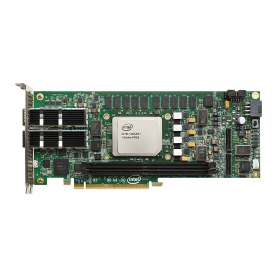
Page 4: Overview
Intel's standard warranty, but reserves the right to make changes to any 9001:2015 products and services at any time without notice. Intel assumes no responsibility or liability arising out of the Registered application or use of any information, product, or service described herein except as expressly agreed to in writing by Intel. - Page 5 Conn +12V from PCIe Gold Fingers Feature Summary • Intel Agilex I-Series (AGIB027) device in the 2957A BGA package — 0.8 VID-adjustable VCC core — R-tile transceivers supporting PCIe Gen5/CXL — F-tile transceivers supporting 56 Gbps NRZ • FPGA configuration —...
- Page 6 — Two DIMM sockets supporting dual DIMM for DDR4 • Communication ports — 2x QSFPDD optical interface port — JTAG header — USB (Micro USB) on-board Intel FPGA Download Cable II — System I2C header • Buttons, switches, and LEDs — System reset push button —...
-
Page 7: Box Contents
1. Overview 683288 | 2022.09.22 1.2. Box Contents Intel Agilex I-Series FPGA Development board, DDR4 DIMM module, USB2.0 Micro- USB cable, 240W power adapter, and NA/EU/JP/UK cords. Note: Intel provides only one DIMM module with each development kit. 1.3. Operating Conditions Table 2. -
Page 8: Getting Started
Intel's standard warranty, but reserves the right to make changes to any 9001:2015 products and services at any time without notice. Intel assumes no responsibility or liability arising out of the Registered application or use of any information, product, or service described herein except as expressly agreed to in writing by Intel. -
Page 9: Installing The Intel Fpga Download Cable Ii Driver
The development board includes integrated Intel FPGA Download Cable II circuits for FPGA programming. However, for the host computer and board to communicate, you must install the on-board Intel FPGA Download Cable II driver on the host computer. Installation instructions for the on-board Intel FPGA Download Cable II driver for your operating system are available on the Intel website. -
Page 10: Development Board Setup
Intel's standard warranty, but reserves the right to make changes to any 9001:2015 products and services at any time without notice. Intel assumes no responsibility or liability arising out of the Registered application or use of any information, product, or service described herein except as expressly agreed to in writing by Intel. -
Page 11: Default Switch And Jumper Settings
3.2.1. Default Setting The Intel Agilex I-Series FPGA Development Kit ships with its board switches preconfigured to support the design examples in the kit. If you suspect your board might not be correctly configured with the default settings, follow the instructions in Table 4 on page 11 to return to its factory settings before proceeding. - Page 12 4: FPGA PMBUS SDM_I2C Bus disable SDM_I2C Bus Enable enable SW5[1:4] OFF/OFF/OFF/X On-board Intel FPGA Download Cable II is the JTAG host when the external JTAG header (J10) is unoccupied. Type 1: JTAG input source PCIe EP Edge On-Board Intel connector...
- Page 13 3. Development Board Setup 683288 | 2022.09.22 Figure 4. SW2[1:4] Switch Setting Figure 5. SW3[1:4] Switch Setting Figure 6. SW4 Switch Setting ® ™ Intel Agilex I-Series FPGA Development Kit User Guide Send Feedback...
- Page 14 QSFPDD_0 connector — QSFPDD_1 connector — USB connector For programming the FPGA using on- board Intel FPGA Download Cable II External JTAG header For use with the external download cable DIMM A connector DDR4/DDRT Dual DIMM A DIMM B connector...
-
Page 15: Perform Board Restore Through Intel Quartus Prime Programmer
3.2.2. Perform Board Restore through Intel Quartus Prime Programmer The development kit ships with FPGA design examples stored in the QSPI flash device and system Intel MAX 10 pre-programmed. If you want to restore board QSPI flash with factory default image, follow these steps: 1. - Page 16 6. Click on the Configuration Device > Add Device to specify the flash device. In the Device list of the pop-up window, select CFI_2Gb for the configuration flash device. ® ™ Intel Agilex I-Series FPGA Development Kit User Guide Send Feedback...
-
Page 17: How To Program The Generated Pof Image
2. Set the DIPSWITCH SW2 to [on:off:off:X] (don't care the 4th bit). 3. Power on the board. 4. Open the Intel Quartus Prime Pro Edition software and click on Tools > Programmer to launch the Programmer tool. 5. In the Hardware Setup page, select AGI FPGA Development Kit, and in the Hardware frequency column, input 16000000 Hz. - Page 18 6. In the Programmer page, click Auto Detect to scan the JTAG devices. 7. Right click the VTAP10 device, Edit > Change Device, change it to MAX 10 > 10M50DAF256. ® ™ Intel Agilex I-Series FPGA Development Kit User Guide Send Feedback...
- Page 19 8. Right click the 10M50DAF256 device, Edit > Attach Flash Device, select Quad SPI Flash Memory QSPI_2Gb. 9. In the Programmer page, click QSPI_2Gb > Change File to select the .pof file. 10. Start the Programmer. ® ™ Intel Agilex I-Series FPGA Development Kit User Guide Send Feedback...
-
Page 20: The Required Smartvid Qsf Assignments To Compile A Design
If you are creating your own design and want to generate programming SRAM object file (.sof), you must add the correct SmartVID setting into the Intel Quartus Prime project for the Intel Agilex FPGA development kit to configure successfully. Before you add the following SmartVID setting into the Quartus settings file (.qsf), you must... - Page 21 -name PWRMGT_SLAVE_DEVICE3_ADDRESS 00 set_global_assignment -name PWRMGT_SLAVE_DEVICE4_ADDRESS 00 set_global_assignment -name PWRMGT_SLAVE_DEVICE5_ADDRESS 00 set_global_assignment -name PWRMGT_SLAVE_DEVICE6_ADDRESS 00 set_global_assignment -name PWRMGT_SLAVE_DEVICE7_ADDRESS 00 set_global_assignment -name PWRMGT_TRANSLATED_VOLTAGE_VALUE_UNIT VOLTS set_global_assignment -name PWRMGT_PAGE_COMMAND_ENABLE OFF ® ™ Intel Agilex I-Series FPGA Development Kit User Guide Send Feedback...
-
Page 22: Board Test System
Intel's standard warranty, but reserves the right to make changes to any 9001:2015 products and services at any time without notice. Intel assumes no responsibility or liability arising out of the Registered application or use of any information, product, or service described herein except as expressly agreed to in writing by Intel. -
Page 23: Download Openjdk
2. Select the JavaFX version 17.0.2. 3. For Windows system, download the JavaFX Windows x64 SDK. 4. For Linux system, download the JavaFX Linux x64 SDK. Figure 12. JavaFX Version ® ™ Intel Agilex I-Series FPGA Development Kit User Guide Send Feedback... -
Page 24: Install Openjdk And Openjfx
683288 | 2022.09.22 4.1.3. Install OpenJDK and OpenJFX You have two downloaded zip files, follow these steps to install them. 1. On Windows system, Intel recommends you to unzip the files and put them in the following directory: C:\Program Files\Java\jre... -
Page 25: Test The Functionality Of The Development Kit
4.2. Test the Functionality of the Development Kit This section describes each control in the BTS. 4.2.1. The Bottom Info Bar The bottom information bar shows the status of the system connection, Intel Quartus Prime version and the JTAG clock. •... -
Page 26: The Sys Info Tab
3. When configuration finishes, the design begins running in the FPGA. The corresponding GUI application tabs that interface with the design are now enabled. If you use the Intel Quartus Prime Programmer for configuration, instead of the BTS GUI, you might need to restart the GUI. -
Page 27: The Gpio Tab
The JTAG chain control shows all the devices currently in the JTAG chain. Note: Change the settings of SW5 to bypass or enable power for Intel MAX 10 and Intel Agilex FPGA. System Intel MAX 10 and FPGA should all be in the JTAG chain when configured and running the BTS GUI. -
Page 28: The Xcvr Tab
4.2.5. The XCVR Tab The XCVR tab allows you to run transceivers tests on your board. You can run the QSFPDD test using optical fiber modules. ® ™ Intel Agilex I-Series FPGA Development Kit User Guide Send Feedback... - Page 29 Detail: Shows the PLL lock and pattern sync status. Control Use the following controls to select an interface to apply PMA settings, data type, and error control: • QSFPDD0 x8 • QSFPDD1 x8 ® ™ Intel Agilex I-Series FPGA Development Kit User Guide Send Feedback...
- Page 30 PRBS23: Pseudo-random 23-bit sequences. • PRBS31: Pseudo-random 31-bit sequences (default). • High_freq: Selects the highest frequency divided-by-2 data pattern 10101010. • Low_freq: Selects the lowest frequency divided-by-33 data pattern. ® ™ Intel Agilex I-Series FPGA Development Kit User Guide Send Feedback...
- Page 31 • Start: This control initiates the loopback tests. • Data Rate: Displays the XCVR type and data rate of each channel. Figure 21. XCVR-Data Rate ® ™ Intel Agilex I-Series FPGA Development Kit User Guide Send Feedback...
-
Page 32: The Ram Tab
4 channels. 4.2.6. The RAM Tab This tab allows you to read and write DDR4-COMP0, DDR4-COMP1, and DDR4-RDIMM memory on your board. Download DDR4 designs through BTS Configure. ® ™ Intel Agilex I-Series FPGA Development Kit User Guide Send Feedback... - Page 33 Offset (Hex): You can define the memory start address to test. • Test Mode: Infinite Read and Write (default), Single Read and Write. • Test Pattern: PRBS (default), User Defined Constant, Walking ‘0’, Walking ‘1'. ® ™ Intel Agilex I-Series FPGA Development Kit User Guide Send Feedback...
- Page 34 Insert error is only enabled during transaction performance analysis. • Clear: Resets the Detected Errors counter and Inserted Errors counter to zeros. Figure 24. The COMP-1 Tab Same with DDR4-COMP0. ® ™ Intel Agilex I-Series FPGA Development Kit User Guide Send Feedback...
-
Page 35: Control On-Board Clock Through Clock Controller Gui
24. It can also be started with the BTS GUI icon “Clock”. The Clock Controller communicates with the System Intel MAX 10 device through either USB port J8 or 10-pin JTAG header J10. Then System Intel MAX 10 controls these programmable clock parts through a 2-wire I C bus. -
Page 36: Monitor On-Board Power Regulator Through Power Monitor Gui
Sets the programmable oscillator frequency for the selected clock to the value in the output controls for the Si5391. Frequency changes might take several OUTx milliseconds to take effect. You might see glitches on the clock during this time. Intel recommends resetting the FPGA logic after changing frequencies. Import Si5391 has a two-time writable non-volatile memory (NVM). -
Page 37: Bts Test Areas
Plug the DDR4 DIMM module which is shipped alone with this development kit in J1/J2. BTS GUI only supports fabric memory interfaces namely DDR4 Comp-CH0, Comp-CH1, and DIMM. ® ™ Intel Agilex I-Series FPGA Development Kit User Guide Send Feedback... - Page 38 4. Board Test System 683288 | 2022.09.22 QSFPDD0/QSFPDD1 Plug QSFPDD0/QSFPDD1 loopback module in J3/J4 before you configure QSFPDD NRZ example build through BTS GUI. ® ™ Intel Agilex I-Series FPGA Development Kit User Guide Send Feedback...
-
Page 39: Revision History
Intel's standard warranty, but reserves the right to make changes to any 9001:2015 products and services at any time without notice. Intel assumes no responsibility or liability arising out of the Registered application or use of any information, product, or service described herein except as expressly agreed to in writing by Intel. - Page 40 Updated the PCIe and CXL Interfaces section. • Updated Figure: Intel Agilex I-Series FPGA Development Board Image—Front. • Updated the header of Table: Intel Agilex I-Series FPGA Development Kit Ordering Information. • Updated Table: Factory Default Switch Settings. • Removed the Factory Reset section.
-
Page 41: Development Kits Components
Intel's standard warranty, but reserves the right to make changes to any 9001:2015 products and services at any time without notice. Intel assumes no responsibility or liability arising out of the Registered application or use of any information, product, or service described herein except as expressly agreed to in writing by Intel. -
Page 42: Intel Agilex I-Series Fpga
To activate the CXL hard IP and receive CXL soft R-Tile Wrapper and Soft Support logic, purchase or activation of a separate CXL IP license is required for proper use with the Intel Quartus Prime Design Software. Contact your local Intel sales representative for pricing details. - Page 43 A. Development Kits Components 683288 | 2022.09.22 Figure 30. MCIO Connector MCIO Connectors for CXL/PCIe Interface ® ™ Intel Agilex I-Series FPGA Development Kit User Guide Send Feedback...
-
Page 44: Mcio Cable Assembly Information
Intel Premier Support and quote ID #14016163317. A.6. Network Interfaces The development kit supports two QSFPDD connectors each, connecting to the Intel Agilex's F-tile (12A) transceivers. Each port can operate at 4x 58G or 8x 28G. These two ports support ZQSFP56 SR optical modules as well as the 3M DAC electrical cables. -
Page 45: Port Controller
RPM jitter <250fs. Figure 32. F-Tile Bank 12A Circuit A.7. Port Controller A Texas Instrument FPC202 dual-port controller serves as the low-speed signal aggregator for the two QSFP ports. ® ™ Intel Agilex I-Series FPGA Development Kit User Guide Send Feedback... -
Page 46: Fpga Configuration
P1_AUX_SDA P1_AUX_SCL FPC202RHUR QFN-58 A.8. FPGA Configuration You can use the Intel Quartus Prime Programmer to configure the FPGA with your SRAM Object File (.sof). FPGA Configuration Setup Ensure the following: • The Intel Quartus Prime Programmer and the Intel FPGA Download Cable II driver are installed on the host computer. -
Page 47: Supported Configuration Modes
The Intel MAX 10 System Controller (U34) interfaces to the Intel Agilex FPGA in the AVST x8 mode. The Intel MAX 10 also interfaces to the QSPI flash in the active serial (AS) x4 mode. For the AS x4 mode,... -
Page 48: Memory Interfaces
Intel MAX 10 Download Cable The on-board Intel FPGA Download Cable II is implemented in an Intel MAX 10 device. A micro-USB connector connects to a CY7C68013A USB2 PHY provides the data to Intel MAX 10. This allows configuration of the FPGA using a USB cable directly connected to a PC running the Intel Quartus Prime software without requiring the external download cable dongle. -
Page 49: I2C
VID regulators, analog-to-digital converters (ADC), and temperature sensors. You can use the Intel Agilex or Intel MAX 10 as the I2C host to access these devices, change clock frequencies or get status information of the board such as voltage and temperature readings. -
Page 50: Clock Circuits
Gen5 by selecting the inputs of a clock multiplex/buffer Si53307. Another input of the clock buffer is from PCIe Edge connector as a system clock of PCIe Gen5. • Si510 provides a 50MHz clock to System Intel MAX 10 and power Intel MAX 10 devices. Figure 36. -
Page 51: Power Guidelines
The power utilization is displayed on a graphical user interface (GUI) that can graph power consumption versus time. A.13.1. Power Guidelines The Intel Agilex I-Series FPGA development kit has two modes of operation as described below. In a Standard PCIe-Compliant System... -
Page 52: Power Distribution System
683288 | 2022.09.22 Figure 38. Powering Board Using Included Power Supply Included Power Supply A.13.2. Power Distribution System The following figure below shows the power distribution system on the Intel Agilex I- Series FPGA development board. ® ™ Intel Agilex... -
Page 53: Power Sequence
Power Sequence Start 1 Group1 2 Group2 3 Group3 A.13.3. Power Sequence Intel Agilex FPGA requires proper power-up sequencing. For more details on the power sequencing groups, refer to Table: Voltage Rails Group in the Intel Agilex Power Management User Guide. -
Page 54: Power Measurement
Group3_PG VCCR_CORE VCCA_PLL A.13.4. Power Measurement Power measurements are provided for six FPGA power rails by reading the power value of various power regulators via their I2C connection. ® ™ Intel Agilex I-Series FPGA Development Kit User Guide Send Feedback... -
Page 55: Temperature Monitoring
THERMn MAX31730ATC+ are brought to the Intel MAX 10 to allow it to immediately sense a temperature fault condition. An over temperature warning LED D9 (Red-colored) is controlled by the Intel MAX 10 device to indicate an over temperature warning. -
Page 56: Board Thermal Requirements
The heatsink is securely mounted to the board using screws for easy assembly and removal. A thermal material is also used between the FPGA and heatsink to ensure good thermal contact. ® ™ Intel Agilex I-Series FPGA Development Kit User Guide Send Feedback... -
Page 57: Board Operating Conditions
85°C A.18. Over Temperature Warning LED A red colored LED (D9) is connected to the Intel MAX 10 to indicate when an over temperature fault condition has been detected. The Intel MAX 10 can turn on this LED to indicate an over temperature warning. -
Page 58: Additional Information
Intel's standard warranty, but reserves the right to make changes to any 9001:2015 products and services at any time without notice. Intel assumes no responsibility or liability arising out of the Registered application or use of any information, product, or service described herein except as expressly agreed to in writing by Intel. -
Page 59: Safety Warnings
To avoid shock, you must ensure that the power cord is connected to a properly wired and grounded receptacle. Ensure that any equipment to which this product is attached to is also connected to properly wired and grounded receptacles. ® ™ Intel Agilex I-Series FPGA Development Kit User Guide Send Feedback... -
Page 60: Safety Cautions
Certain components such as heat sinks, power regulators, and processors may be hot. Heatsink fans are not guarded. Power supply fan may be accessible through guard. Care should be taken to avoid contact with these components. ® ™ Intel Agilex I-Series FPGA Development Kit User Guide Send Feedback... - Page 61 Public Switched Telecommunication Network (PSTN) as it might result in disruption of the network. No formal telecommunication certification to FCC, R&TTE Directive, or other national requirements have been obtained. ® ™ Intel Agilex I-Series FPGA Development Kit User Guide Send Feedback...
- Page 62 Failure to use wrist straps can damage components within the system. Attention: Please return this product to Intel for proper disposition. If it is not returned, refer to local environmental regulations for proper recycling. Do not dispose of this product in unsorted municipal waste.
-
Page 63: Compliance Information
B. Additional Information 683288 | 2022.09.22 Please return this product to Intel for proper disposition. If it is not returned, refer to local environmental regulations for proper recycling. Do not dispose of product in unsorted municipal waste. B.2. Compliance Information...
Need help?
Do you have a question about the Agilex I Series and is the answer not in the manual?
Questions and answers