Intel Agilex 7 FPGA I Series User Manual
Transceiver-soc development kit
Hide thumbs
Also See for Agilex 7 FPGA I Series:
- User manual (79 pages) ,
- User manual (68 pages) ,
- User manual (59 pages)

Related Manuals for Intel Agilex 7 FPGA I Series


Summary of Contents for Intel Agilex 7 FPGA I Series
- Page 1 ® Intel Agilex 7 FPGA I-Series Transceiver-SoC Development Kit User Guide 721605 Online Version Send Feedback Version: 2023.04.10...
-
Page 2: Table Of Contents
5.4.1. HPS Out of Box Experience (OOBE) Daughter Card........40 6. Custom Projects for the Development Kit..............41 6.1. Add SmartVID Settings in the Intel Quartus Prime QSF File........41 6.2. Golden Top......................42 7. Document Revision History for the Intel Agilex 7 FPGA I-Series Transceiver-SoC Development Kit User Guide.................. - Page 3 A.7. Daughter Cards....................60 A.8. Connectors and Cables..................61 B. Additional Information....................62 B.1. Safety and Regulatory Information.................62 B.1.1. Safety Warnings..................63 B.1.2. Safety Cautions..................64 B.2. Compliance Information..................67 ® Intel Agilex 7 FPGA I-Series Transceiver-SoC Development Kit User Guide Send Feedback...
-
Page 4: Overview
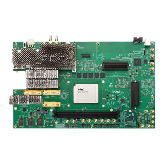
Intel's standard warranty, but reserves the right to make changes to any 9001:2015 products and services at any time without notice. Intel assumes no responsibility or liability arising out of the Registered application or use of any information, product, or service described herein except as expressly agreed to in writing by Intel. - Page 5 1. Overview 721605 | 2023.04.10 Figure 1. Intel Agilex 7 FPGA I-Series Transceiver-SoC Development Kit Board Image - ® DK-SI-AGI027FB and DK-SI-AGI027FES (Intel Enpirion Figure 2. Intel Agilex 7 FPGA I-Series Transceiver-SoC Development Kit Board Image - ® DK-SI-AGI027FA and DK-SI-AGI027FC (Not Intel Enpirion...
-
Page 6: Block Diagram
1. Overview 721605 | 2023.04.10 1.1. Block Diagram Figure 3. Intel Agilex 7 FPGA I-Series Transceiver-SoC Development Kit Block Diagram 1.2. Feature Summary • Intel Agilex 7 FPGA I-Series, 2.7M LE, 3184B package • F-Tile 1 (13C) — 4 FHT transceiver channels fan out to Quad Small Form Factor Double Density 800 (QSFPDD800) —... -
Page 7: Box Contents
8GB SR DDR4-2666 (x72 w/ ECC) component down (HPS) • IO48 interface for HPS Out of Box Experience (OOBE) daughter cards 1.3. Box Contents • Intel Agilex 7 FPGA I-Series Transceiver-SoC Development Kit • Single-rank DDR4 DIMM module • QSPI flash daughter card •... -
Page 8: Getting Started
Intel's standard warranty, but reserves the right to make changes to any 9001:2015 products and services at any time without notice. Intel assumes no responsibility or liability arising out of the Registered application or use of any information, product, or service described herein except as expressly agreed to in writing by Intel. - Page 9 Design Examples: Memory, XCVR, GPIO, System Intel MAX 10 The original data programmed into flash U85 for AVST x32 factory_recovery configuration and System Intel MAX 10 before shipment. Use this data to restore the board with its original factory content. ®...
-
Page 10: Power Up The Development Kit
Intel's standard warranty, but reserves the right to make changes to any 9001:2015 products and services at any time without notice. Intel assumes no responsibility or liability arising out of the Registered application or use of any information, product, or service described herein except as expressly agreed to in writing by Intel. -
Page 11: Power Up
D22 LED illuminates, indicating that the board power up successfully. If the LED (D22) is not turned ON, it indicates that one or more power supply is incorrect. ® Intel Agilex 7 FPGA I-Series Transceiver-SoC Development Kit User Guide Send Feedback... -
Page 12: Perform Board Restore
This development kit ships with GHRD design examples stored in the QSPI flash device and system Intel MAX 10 pre-programmed. You must perform board restore by using the restore menu in BTS GUI or following the instructions below through the Intel Quartus Prime Programmer GUI. -
Page 13: Board Test System
Intel's standard warranty, but reserves the right to make changes to any 9001:2015 products and services at any time without notice. Intel assumes no responsibility or liability arising out of the Registered application or use of any information, product, or service described herein except as expressly agreed to in writing by Intel. -
Page 14: Set Up Bts Gui Running Environment
4. Board Test System 721605 | 2023.04.10 ® Figure 5. BTS GUI (Not Intel Enpirion ) DK-SI-AGI027FA and DK-SI-AGI027FC 4.1. Set Up BTS GUI Running Environment To run BTS GUI, including Power Monitor and Clock Controller GUI, you need to download and install Java runtime including OpenJDK and OpenJFX on your systems and set up the running environment. -
Page 15: Download Openjfx
4. For Linux system, download the JavaFX Linux x64 SDK. 4.1.3. Install OpenJDK and OpenJFX You have two downloaded zip files, follow these steps to install them. 1. On Windows system, Intel recommends you to unzip the files and put them in the following directory: — C:\Program Files\Java\jre —... -
Page 16: Run Bts Gui
Power Up Development Kit. In most cases, BTS requires system Intel MAX 10 and Intel Agilex 7 FPGA on the JTAG chain while Clock Controller and Power Monitor require only System Intel MAX 10. 3. Check the external modules status: MXPM cable/QSFP/QSFPDD/FMC/DIMM 4. -
Page 17: Test The Functionality Of The Development Kit
4.2. Test the Functionality of the Development Kit This section describes each control in the BTS. 4.2.1. The Bottom Info Bar The bottom information bar shows the status of the system connection, the Intel Quartus Prime version and the JTAG clock. •... -
Page 18: The Sys Info Tab
3. When configuration finishes, the design begins running in the FPGA. The corresponding GUI application tabs that interface with the design are now enabled. If you use the Intel Quartus Prime Programmer for configuration, instead of the BTS GUI, you might need to restart the GUI. -
Page 19: The Gpio Tab
JTAG Chain The JTAG chain control shows all the devices currently in the JTAG chain. Note: You should place the system Intel MAX 10 and FPGA in the JTAG chain when running the BTS GUI. 4.2.4. The GPIO Tab The GPIO tab allows you to interact with all the general-purpose user I/O components on your board. - Page 20 The Push Button control shows the status of PB0 and PB1. Qsys Memory Map The Qsys Memory Map control shows the memory map of bts_config.sof design running on your board. ® Intel Agilex 7 FPGA I-Series Transceiver-SoC Development Kit User Guide Send Feedback...
-
Page 21: The Xcvr Tab
• Detail: Shows the PLL lock and pattern sync status of each channel. The number of the error bits of each channel can be found here. ® Intel Agilex 7 FPGA I-Series Transceiver-SoC Development Kit User Guide Send Feedback... - Page 22 QSFPDD NRZ-PMA Setting Data Type The Data Type control specifies the type of data pattern contained in the transactions. Select the following available data types for analysis: ® Intel Agilex 7 FPGA I-Series Transceiver-SoC Development Kit User Guide Send Feedback...
- Page 23 Data Rate: Displays the XCVR type and data rate of each channel. Figure 15. QSFPDD NRZ - Data Rate 4.2.5.2. The QSFPDD PAM4 Tab Similar control functions with the QSFPDD NRZ tab. ® Intel Agilex 7 FPGA I-Series Transceiver-SoC Development Kit User Guide Send Feedback...
- Page 24 721605 | 2023.04.10 Figure 16. The QSFPDD PAM4 Tab 4.2.5.3. The FMCA NRZ Tab Similar control functions with the QSFPDD NRZ tab except for the port selection. ® Intel Agilex 7 FPGA I-Series Transceiver-SoC Development Kit User Guide Send Feedback...
- Page 25 721605 | 2023.04.10 Figure 17. The FMCA NRZ Tab 4.2.5.4. The FMCB NRZ Tab Similar control functions with the QSFPDD NRZ tab except for the port selection. ® Intel Agilex 7 FPGA I-Series Transceiver-SoC Development Kit User Guide Send Feedback...
- Page 26 4. Board Test System 721605 | 2023.04.10 Figure 18. The FMCB NRZ Tab 4.2.5.5. The QSFPDD800 PAM4 Tab Similar control functions with the QSFPDD NRZ tab. ® Intel Agilex 7 FPGA I-Series Transceiver-SoC Development Kit User Guide Send Feedback...
- Page 27 4. Board Test System 721605 | 2023.04.10 Figure 19. The QSFPDD800 PAM4 Tab Figure 20. The QSFPDD800 PAM4 Tab - PMA Setting ® Intel Agilex 7 FPGA I-Series Transceiver-SoC Development Kit User Guide Send Feedback...
- Page 28 21 4.2.5.6. The MXPM NRZ Tab Similar control functions with the QSFPDD NRZ tab except for the port selection. Figure 21. The MXPM NRZ Tab ® Intel Agilex 7 FPGA I-Series Transceiver-SoC Development Kit User Guide Send Feedback...
- Page 29 4.2.5.7. The MXPM PAM4 Tab Similar control functions with the QSFPDD NRZ tab. Figure 22. The MXPM PAM4 Tab 4.2.5.8. The SDI Tab Similar control functions with the QSFPDD NRZ tab. ® Intel Agilex 7 FPGA I-Series Transceiver-SoC Development Kit User Guide Send Feedback...
-
Page 30: The Memory Tab
This tab allows you to read and write DDR4 DIMM-2A (DIMM-I) and DDR4 DIMM-2B (DIMM-II) memory on your board. RDIMMS only tests DIMM-II while RDIMMD tests DIMM-I and DIMM-II. Download the design through BTS Configure. ® Intel Agilex 7 FPGA I-Series Transceiver-SoC Development Kit User Guide Send Feedback... - Page 31 Write (MBps) and Read (MBps): Show the number of bytes analyzed per second. • Data Bus: 72 bits (8 bits ECC) wide, reference clock is 166.666 MHz, and the frequency is 1333.33 MHz double data rate 2666.66 MT/s. ® Intel Agilex 7 FPGA I-Series Transceiver-SoC Development Kit User Guide Send Feedback...
- Page 32 Clear: Resets the Detected Errors counter and Inserted Errors counter to zeros. Figure 25. The RDIMMD Tab Similar with RDIMMS. Test Size can be set to 32 GB with two RDIMMs. ® Intel Agilex 7 FPGA I-Series Transceiver-SoC Development Kit User Guide Send Feedback...
-
Page 33: Control On-Board Clock Through Clock Controller Gui
BTS GUI icon “Clock”. The clock controller communicates with the system Intel MAX 10 device through a 10- pin JTAG header J11 or USB port J10. Then, system Intel MAX 10 controls these programmable clock parts through a 2-wire I C bus. - Page 34 Sets the programmable oscillator frequency for the selected clock to the value in the output controls for Si5394. Frequency changes might take several milliseconds OUTx to take effect. You might see glitches on the clock during this time. Intel recommends resetting the FPGA logic after changing frequencies. Import Si5394 has a two-time rewritable non-volatile memory (NVM).
- Page 35 4. Board Test System 721605 | 2023.04.10 Figure 28. Si5391-B Same with Si5391-A. ® Intel Agilex 7 FPGA I-Series Transceiver-SoC Development Kit User Guide Send Feedback...
- Page 36 5 output frequency families. Import ZL30733 has a multiple time writable non-volatile memory (NVM). You can generate the register list with the following format: ® Intel Agilex 7 FPGA I-Series Transceiver-SoC Development Kit User Guide Send Feedback...
-
Page 37: Monitor On-Board Power Regulator Through Power Monitor Gui
PCB. The Power Monitor GUI communicates with System Intel MAX 10 through a 10-pin JTAG header J11 or USB port J10. System Intel MAX 10 monitors and controls power regulator, temperature/voltage/current sensing chips through a 2-wire I C bus. -
Page 38: Bts Test Areas
Plug the DIMM-I/II module which is shipped alone with this development kit in J5. The BTS GUI only supports fabric memory interfaces namely DDR4 DIMM-2A (DIMM-I) and DDR4 DIMM-2B (DIMM-II). ® Intel Agilex 7 FPGA I-Series Transceiver-SoC Development Kit User Guide Send Feedback... -
Page 39: Development Kit Hardware And Configuration
Intel's standard warranty, but reserves the right to make changes to any 9001:2015 products and services at any time without notice. Intel assumes no responsibility or liability arising out of the Registered application or use of any information, product, or service described herein except as expressly agreed to in writing by Intel. -
Page 40: Daughter Cards
5. Development Kit Hardware and Configuration 721605 | 2023.04.10 1. Set S9 to Avalon-ST x32 mode first. 2. Default system Intel MAX 10 image support the Avalon-ST x32 mode only. You should build a corresponding image if you select Avalon-ST x8 or Avalon-ST .POF... -
Page 41: Custom Projects For The Development Kit
Intel's standard warranty, but reserves the right to make changes to any 9001:2015 products and services at any time without notice. Intel assumes no responsibility or liability arising out of the Registered application or use of any information, product, or service described herein except as expressly agreed to in writing by Intel. -
Page 42: Golden Top
You can use the Golden Top project as the starting point for your designs. It comes loaded with constraints, pin locations, defined I/O standard, direction, and general termination. The DDR4 pin termination settings are not included. Refer DDR4 example designs for details. ® Intel Agilex 7 FPGA I-Series Transceiver-SoC Development Kit User Guide Send Feedback... -
Page 43: Document Revision History For The Intel Agilex 7 Fpga I-Series Transceiver-Soc Development Kit User Guide
Intel's standard warranty, but reserves the right to make changes to any 9001:2015 products and services at any time without notice. Intel assumes no responsibility or liability arising out of the Registered application or use of any information, product, or service described herein except as expressly agreed to in writing by Intel. - Page 44 7. Document Revision History for the Intel Agilex 7 FPGA I-Series Transceiver-SoC Development Kit User Guide 721605 | 2023.04.10 Document Changes Version • Updated the Perform Board Restore section. • Updated step 3 in the Restore Board QSPI Flash with Default Factory Image section.
-
Page 45: Development Kit Components
Intel's standard warranty, but reserves the right to make changes to any 9001:2015 products and services at any time without notice. Intel assumes no responsibility or liability arising out of the Registered application or use of any information, product, or service described herein except as expressly agreed to in writing by Intel. - Page 46 Mode S20 [4:2] S19 [4] [3] [2] [1] Function ON: Bypass from chain OFF: Enable in chain Mode 3: External Intel FPGA Download Cable act as the only JTAG Master. Chained HPS with SDM nodes internally. ON/ON/OFF SDM is always enabled in Mode 2: On-board Intel the JTAG chain.
-
Page 47: Power
A. Development Kit Components 721605 | 2023.04.10 A.2. Power Figure 32. Power Tree (Intel Enpirion) DK-SI-AGI027FB and DK-SI-AGI027FES 3.3V_STB 12V_DCIN VCCERT1_FHT_GXF_U20 FPGA LTM4625 ADP1765A P1V0_VCCERT1_U20_EN PWR_M10/ SYS_M10 / FLASH / VCCERT1_FHT_GXF_U20 CONN 4.33A@1.0V 1.8V_STB UBII PHY / CLK GEN EM5V... - Page 48 A. Development Kit Components 721605 | 2023.04.10 Figure 33. Power Tree (Not Intel Enpirion) DK-SI-AGI027FA and DK-SI-AGI027FC 3.3V_STB 12V_DCIN VCCERT1_FHT_GXF_13A FPGA LTM4625 ADP1765A P1V0_VCCERT1_13A_EN 3.44A PWR_M10/ SYS_M10 / FLASH / VCCERT1_FHT_GXF_13A CONN 3.05A@1.0V 1.8V_STB UBII PHY / CLK GEN LTM4668 1.78A...
- Page 49 Onboard hot-plug circuit shuts down all power rails when the total power is over 360 W (30 A). UB2/PWR Intel MAX 10 shuts down significant power rails when one or more good power indicators is low due to a power fault.
-
Page 50: Clocks
Si5391_B_OUT_P6/N6 148.5M Si5391_B_OUT_P7/N7 368.63M Si5391_B_OUT_P9/N9 153.6M CLK_13A_FGT_REFCLK3_P/N 153.6M CLK_FHT_13A_P_0/N_0 156.25M CLK_FHT_13C_P_0/N_0 156.25M CLK_FGT_13C_REFCLK_2P/N 135M CLK_A_12C_FGT_P_0/N_0 100M CLK_3A_GPIO_P_0/N_0 100M CLK_A_12C_FGT_P_3/N_3 148.5M CLK_3A_GPIO_P_2/N_2 148.5M CLK_A_12C_FGT_P_2/N_2 156.25M CLK_3A_GPIO_P_1/N_1 156.25M continued... ® Intel Agilex 7 FPGA I-Series Transceiver-SoC Development Kit User Guide Send Feedback... - Page 51 ETH_REFCLK_156.25M_P/N 156.25M CPRI_REFCLK_153.6M_P/N 153.6M CPRI_REFCLK_184.32M_P/N 184.32M FMCA_REFCLK_148.5M_P/N 148.5M FMCA_REFCLK_156.25M_P/N 156.25M Si5391_A_156.25M_REFIN_P/N 156.25M Si5391_B_156.25M_REFIN_P/N 156.25M CLK_3C_GPIO_P_1/N_1 156.25M CLK_B_12A_FGT_P_3/N_3 148.5M CLK_3C_GPIO_P_0/N_0 148.5M 1PPS_FPGA_CLK 1PPS 1PPS_SMA_OUT 1PPS 10MHz_SMA_OUT ZL_SPARE_CLK_100M 100M ® Intel Agilex 7 FPGA I-Series Transceiver-SoC Development Kit User Guide Send Feedback...
-
Page 52: General Input/Output
MAX 10 CTRL/STAT Si5391 Recovered_CLK Recovered_CLK REFCLK9 REFCLK9 FMC_RCVD_CLK (ZL-REFIN2) A.4. General Input/Output Table 10. Intel MAX 10 and FPGA Schematic Signal Name Description The value of filtered F_GPIO0 user_pb[0] The value of filtered F_GPIO1 user_pb[1] in RP mode F_GPIO2... - Page 53 After power ok: , =1 by default S_control_gui[15] Before power ok: 1 usb_mux_reset After power ok: , =0 by default S_control_gui[16] : controlled by mux_sel0 system_info_slv_data_write_0[0]=1 system_info_slv_data_write_1[0] continued... ® Intel Agilex 7 FPGA I-Series Transceiver-SoC Development Kit User Guide Send Feedback...
- Page 54 : controlled by mux_sel10 system_info_slv_data_write_0[10]=1 system_info_slv_data_write_1[10] : controlled by system_info_slv_data_write_0[10]=0 MUX_DIP_SW4 : controlled by mux_sel11 system_info_slv_data_write_0[11]=1 system_info_slv_data_write_1[11] : controlled by system_info_slv_data_write_0[11]=0 MUX_DIP_SW5 : controlled by mux_sel12 system_info_slv_data_write_0[12]=1 system_info_slv_data_write_1[12] continued... ® Intel Agilex 7 FPGA I-Series Transceiver-SoC Development Kit User Guide Send Feedback...
- Page 55 UB2/PWR Intel MAX 10 Schematic Signal Name Description FPGA Power Good FPGA_POK_LED Reserved GPIO between System Intel MAX 10 and Power SYS_PWR_RSV0 Intel MAX 10. Used as I C clock. Reserved GPIO between System Intel MAX 10 and Power SYS_PWR_RSV1 Intel MAX 10.
-
Page 56: Memory Interfaces
A.6. Communication Interfaces MCIO Port The MCIO slot is a PCIe Gen4 x4 port which fans out from Intel Agilex 7 FPGA I-Series F-Tile. This port is designed to meet the standard MCIO pinout. System Intel MAX 10 acts as the board management controller (BMC) of the development kit. It manages power-up reset for both PCIe root port and PCIe endpoint. - Page 57 Intel Agilex 7 I-Series Development Kit supports 1x QSFPDD800 port. QSFDD800 port fans out from Intel Agilex 7 FPGA I-Series F-Tile (FHT). The FHT tile from bank 13A and 13C can run up to 116G PAM4. 4 FHT lanes from bank 13C is terminated directly to QSFPDD800 connector lanes (J22).
- Page 58 FPGA MXPM CONN (J2) MXPM CONN (J8) QSFPDD800 CONN (J22) MXP port fan out from Intel Agilex 7 FPGA I-Series F-Tile (13A). All four channels can run up to 32G NRZ and 58G PAM4. Table 17. Schematic Signal Name Description...
- Page 59 C master instance from system Intel MAX 10 ( VCXO_I2C_SDA/SCL controls the on board VCXO and Si5394 clock generator. Intel Agilex 7 FPGA also manages QSFPDD800, 2x QSFPDD, 2DPC DIMM I C buses, SDI transceivers, and ZL30733 clock synthesizer device.
-
Page 60: Daughter Cards
A. Development Kit Components 721605 | 2023.04.10 Figure 38. C Serial Bus (Not Intel Enpirion) DK-SI-AGI027FA and DK-SI-AGI027FC LTC2497 LTC2497 I-Sense I-Sense IVSNS_I2C_SDA/SCL CY7C88013A I2C @3.3V @3.3V MAX31730 MAX31730 ATC+ ATC+ T_SNS_SDA/SCL I2C @3.3V LTM4677 LTM4686 LTM4677 LTM4677 LTM4677 P1V2_IO... -
Page 61: Connectors And Cables
J2 – J8 Connect between J2 and J8 MCIO cable HMC74-0631 (Amphenol) — HD-BNC Straight Plug to HD- 095-850-214M100 SDI loopback between J1 BNC Straight Plug (Amphenol) and J32 ® Intel Agilex 7 FPGA I-Series Transceiver-SoC Development Kit User Guide Send Feedback... -
Page 62: Additional Information
Intel's standard warranty, but reserves the right to make changes to any 9001:2015 products and services at any time without notice. Intel assumes no responsibility or liability arising out of the Registered application or use of any information, product, or service described herein except as expressly agreed to in writing by Intel. -
Page 63: Safety Warnings
To avoid shock, you must ensure that the power cord is connected to a properly wired and grounded receptacle. Ensure that any equipment to which this product is attached to is also connected to properly wired and grounded receptacles. ® Intel Agilex 7 FPGA I-Series Transceiver-SoC Development Kit User Guide Send Feedback... -
Page 64: Safety Cautions
Certain components such as heat sinks, power regulators, and processors may be hot. Heatsink fans are not guarded. Power supply fan may be accessible through guard. Care should be taken to avoid contact with these components. ® Intel Agilex 7 FPGA I-Series Transceiver-SoC Development Kit User Guide Send Feedback... - Page 65 Public Switched Telecommunication Network (PSTN) as it might result in disruption of the network. No formal telecommunication certification to FCC, R&TTE Directive, or other national requirements have been obtained. ® Intel Agilex 7 FPGA I-Series Transceiver-SoC Development Kit User Guide Send Feedback...
- Page 66 Failure to use wrist straps can damage components within the system. Attention: Please return this product to Intel for proper disposition. If it is not returned, refer to local environmental regulations for proper recycling. Do not dispose of this product in unsorted municipal waste.
-
Page 67: Compliance Information
B. Additional Information 721605 | 2023.04.10 Please return this product to Intel for proper disposition. If it is not returned, refer to local environmental regulations for proper recycling. Do not dispose of product in unsorted municipal waste. B.2. Compliance Information...
Need help?
Do you have a question about the Agilex 7 FPGA I Series and is the answer not in the manual?
Questions and answers