Quectel BG95 A-GL Series Hardware Design
Lpwa module
Hide thumbs
Also See for BG95 A-GL Series:
- Hardware design (84 pages) ,
- Application note (57 pages) ,
- Manual (48 pages)

Related Manuals for Quectel BG95 A-GL Series


Summary of Contents for Quectel BG95 A-GL Series
- Page 1 BG95xA-GL Hardware Design LPWA Module Series Version: 1.1.1 Date: 2022-06-10 Status: Preliminary...
- Page 2 LPWA Module Series At Quectel, our aim is to provide timely and comprehensive services to our customers. If you require any assistance, please contact our headquarters: Quectel Wireless Solutions Co., Ltd. Building 5, Shanghai Business Park Phase III (Area B), No.1016 Tianlin Road, Minhang District, Shanghai...
- Page 3 Except as otherwise set forth herein, nothing in this document shall be construed as conferring any rights to use any trademark, trade name or name, abbreviation, or counterfeit product thereof owned by Quectel or any third party in advertising, publicity, or other aspects.
- Page 4 Manufacturers of the cellular terminal should notify users and operating personnel of the following safety information by incorporating these guidelines into all manuals of the product. Otherwise, Quectel assumes no liability for customers’ failure to comply with these precautions.
- Page 5 LPWA Module Series About the Document Revision History Version Date Author Description Lex LI/ 2021-07-07 Creation of the document Ben JIANG Lex LI/ 2022-04-22 First official release Ben JIANG Preliminary: Lex LI/ 1.1.0 2022-05-30 Added the applicable modules of BG953A-GL and Ben JIANG BG955A-GL.
-
Page 6: Table Of Contents
LPWA Module Series Contents Safety Information ............................3 About the Document ............................ 4 Contents .................................5 Table Index ..............................8 Figure Index ..............................10 Introduction ............................12 1.1. Special Mark ..........................12 Product Overview ..........................13 2.1. Frequency Bands and Functions ..................... 14 2.2. Key Features .......................... - Page 7 LPWA Module Series 4.4. ADC Interfaces ......................... 56 4.5. Indication Signals ........................57 4.5.1. PSM Status Indication .....................57 4.5.2. Network Status Indication ....................58 4.5.3. STATUS ........................... 59 4.5.4. MAIN_RI .......................... 60 4.6. GRFC Interfaces ........................60 4.7. GPIO Interface ..........................61 4.8.
- Page 8 LPWA Module Series 8.3. Packaging Specifications ......................113 8.3.1. Carrier Tape ........................113 8.3.2. Plastic Reel ........................114 8.3.3. Packing Process ......................115 Appendix References ........................116 BG95xA-GL_Hardware_Design 7 / 102...
- Page 9 LPWA Module Series Table Index Table 1: Special Mark ...........................12 Table 2: Brief Introduction of the Module .....................13 Table 3: Wireless Network Types ........................ 14 Table 4: Key Features ..........................15 Table 5: I/O Parameters Definition ......................25 Table 6: Pin Definition – Pins with Same Functions on BG95xA-GL ............25 Table 7: Pin Definition –...
- Page 10 LPWA Module Series Table 42: BG951A-GL GNSS Performance ....................72 Table 43: BG955A-GL GNSS Performance ....................72 Table 44: Antenna Design Requirements ....................77 Table 45: Absolute Maximum Ratings ......................89 Table 46: BG950A-GL & BG951A-GL & BG953A-GL Power Supply Ratings ..........90 Table 47: BG955A-GL Power Supply Ratings .....................90...
- Page 11 LPWA Module Series Figure Index Figure 1: Functional Diagram of BG950A-GL ..................... 18 Figure 2: Functional Diagram of BG951A-GL ..................... 19 Figure 3: Functional Diagram of BG953A-GL ..................... 20 Figure 4: Functional Diagram of BG955A-GL ..................... 21 Figure 5: Pin Assignment of BG950A-GL & BG953A-GL (Top View) ............
- Page 12 LPWA Module Series Figure 42: Recommended Footprint (Top View, Unit: mm) ...............109 Figure 43: Top & Bottom Views of BG95xA-GL ..................110 Figure 44: Recommended Reflow Soldering Thermal Profile ..............112 Figure 45: Carrier Tape Dimension Drawing ..................... 114 Figure 46: Plastic Reel Dimension Drawing ....................
-
Page 13: Introduction
LPWA Module Series Introduction This document helps you gain a quick insight into BG95xA-GL modules, their air and hardware interfaces, electrical and mechanical specifications, and other related information, as well. In addition, it includes some reference designs that, coupled with application notes and user guides, facilitate the development and deployment of your LPWA module applications. -
Page 14: Product Overview
LPWA Module Series Product Overview The module is an embedded IoT (LTE Cat M1, NB1/NB2*) wireless communication module. It supports data connectivity on LTE HD-FDD network, and features GNSS functionality to meet your specific application demands. Additionally, BG955A-GL also supports GPRS network. It is an SMD type module that can be engineered into M2M applications, such as smart metering, tracking system, security, wireless POS, and other wearable devices. -
Page 15: Frequency Bands And Functions
LPWA Module Series 2.1. Frequency Bands and Functions Table 3: Wireless Network Types Module Supported Bands LTE Bands Power Class GNSS Cat M1: LTE HD-FDD: B1/B2/B3/B4/B5/B8/B12/B13/B18/B19/B2 0/B25/B26/B27/B28/B66 Power Class 3 GPS, BG950A-GL NB1/NB2* (23 dBm ±2.7 dB) GLONASS. LTE HD-FDD: B1/B2/B3/B4/B5/B8/B12/B13/B17/B18/B1 9/B20/B25/B28/B66 Cat M1:... -
Page 16: Key Features
LPWA Module Series NOTE The baseband chip of BG950A-GL, BG953A-GL and BG955A-GL integrates the GNSS function, whereas the internal baseband chip and GNSS chip are separated on BG951A-GL. Therefore, BG951A-GL supports concurrent operation of LTE and GNSS, whereas BG950A-GL, BG953A-GL and BG955A-GL does not. - Page 17 Network Indication Pin NET_STATUS to indicate network connectivity status 3GPP TS 27.007 and 3GPP TS 27.005 AT commands AT Commands Quectel enhanced AT commands Main antenna interface (ANT_MAIN), 50 Ω impedance Antenna Interface GNSS antenna interface (ANT_GNSS), 50 Ω impedance ...
-
Page 18: Functional Diagram
LPWA Module Series Supports PPP/TCP/UDP/SSL/MQTT/FTP(S)/HTTP(S)/LwM2M/IPv4/IPv6/ Internet Protocol TLS/DTLS/PING/CoAP/NITZ protocols Features Supports PAP and CHAP for PPP connections BG950A-GL/BG953A-GL/BG955A-GL: GPS, GLONASS GNSS Features BG951A-GL: GPS, GLONASS, BDS, Galileo, QZSS Operating temperature range : -35 to +75 °C ... - Page 19 LPWA Module Series Figure 1: Functional Diagram of BG950A-GL BG95xA-GL_Hardware_Design 18 / 102...
- Page 20 LPWA Module Series Figure 2: Functional Diagram of BG951A-GL BG95xA-GL_Hardware_Design 19 / 102...
- Page 21 LPWA Module Series Figure 3: Functional Diagram of BG953A-GL BG95xA-GL_Hardware_Design 20 / 102...
- Page 22 LPWA Module Series Figure 4: Functional Diagram of BG955A-GL BG95xA-GL_Hardware_Design 21 / 102...
-
Page 23: Pin Assignment
LPWA Module Series 2.4. Pin Assignment The following figure illustrates the pin assignment of BG950A-GL and BG953A-GL. Figure 5: Pin Assignment of BG950A-GL & BG953A-GL (Top View) BG95xA-GL_Hardware_Design 22 / 102... - Page 24 LPWA Module Series The following figure illustrates the pin assignment of BG951A-GL. Figure 6: Pin Assignment of BG951A-GL (Top View) BG95xA-GL_Hardware_Design 23 / 102...
- Page 25 LPWA Module Series The following figure illustrates the pin assignment of BG955A-GL. Figure 7: Pin Assignment of BG955A-GL (Top View) NOTE ADC input voltage must not exceed 1.8 V. Keep all RESERVED pins and unused pins unconnected. GND pins should be connected to ground in the design. Only BG951A-GL supports GNSS_BOOT (pin 75), GNSS_NRST (pin 76), GNSS_EN (pin 97) and BG95xA-GL_Hardware_Design 24 / 102...
-
Page 26: Pin Description
LPWA Module Series SFNIND_1PPS (pin 98). On BG950A-GL, BG953A-GL and BG955A-GL, pin 27 (CLI_TXD1) and pin 28 (CLI_RXD1) are connected to pin 95 (CLI_TXD2) and pin 94 (CLI_RXD2) respectively inside the module. The LNA is integrated inside the module. It is not recommended to use an external LNA. It is strongly recommended to keep GNSS_LNA_EN (pin 51) and VDD_RF (pin 99) unconnected. - Page 27 LPWA Module Series Internally pulled up max = 0.3 V PWRKEY Turn on/off the module with a 470 kΩ min = 1.0 V resistor. Reset Pin Name Description DC Characteristics Comment Internally pulled up max = 0.3 V RESET_N Reset the module with a 470 kΩ...
- Page 28 LPWA Module Series min = 1.26 V max = 2.0 V max = 0.36 V min = 1.44 V max = 0.36 V USIM_CLK (U)SIM card clock min = 1.44 V Specified ground for USIM_GND (U)SIM card Main UART Interface Pin Name Description DC Characteristics...
- Page 29 LPWA Module Series 50 Ω impedance. ANT_GNSS GNSS antenna interface If unused, keep this pin open. GPIO Interfaces Pin Name Description DC Characteristics Comment GPIO1 GPIO2 GPIO3 max = 0.36 V GPIO4 min = 1.44 V 1.8 V power General-purpose min = -0.2 V domain.
- Page 30 LPWA Module Series min = -0.2 V 1.8 V power Application processor max = 0.54 V domain. AP_READY sleep state detect min = 1.26 V If unused, keep this max = 2.0 V pin open. Used for main UART min = -0.2 V 1.8 V power function control and for max = 0.3 V...
- Page 31 LPWA Module Series Table 7: Pin Definition – Pins with Different Functions on BG95xA-GL BG950A-GL/BG953A-GL BG951A-GL BG955A-GL DC Characteristics Comment Pin Name Pin Description Pin Name Pin Description Pin Name Pin Description Power supply for the Power supply for the module’s BG950A-GL/BG953A-GL: VBAT_BB VBAT_BB...
-
Page 32: Evb Kit
Keep all RESERVED pins and unused pins unconnected. 2.6. EVB Kit To help you develop applications with the module, Quectel supplies an evaluation board (UMTS<E EVB) with accessories to control or test the module. For more details see document [1]. -
Page 33: Operating Characteristics
LPWA Module Series Operating Characteristics 3.1. Operating Modes The table below outlines operating modes of the module. Table 8: Operating Mode Overview Mode Details The module remains registered on the network and is ready to send Idle and receive data. In this mode, the software is active. Normal Operation The module is connected to the network. - Page 34 LPWA Module Series NOTE In e-I-DRX mode, it is recommended to use the main UART interface for data communication, as the use of USB interface will increase power consumption. 3.2. Airplane Mode When the module enters airplane mode, the RF function will be disabled, and all AT commands correlative with RF function will be inaccessible.
-
Page 35: Extended Idle Mode Drx (E-I-Drx)
LPWA Module Series PSM use. If the module wants to change the Active Time value, the module consequently requests the value it wants in the TAU procedure. If PSM is supported by the network, then it can be enabled via AT+QPSMS. In this case, driving PON_TRIG low will set the module to PSM. -
Page 36: E-I-Drx Sleep Mode
LPWA Module Series 3.4.1. e-I-DRX Sleep Mode If e-I-DRX is supported by the network, perform the steps below in sequence to make the module enter e-l-DRX sleep mode, in which case the main UART interface is inaccessible. Send AT+QPSMS=0 to disable the use of PSM. Send AT+CEDRXS=1 to enable the use of e-l-DRX. - Page 37 LPWA Module Series Send AT+CFUN=0 to set the module to minimum functionality Drive MAIN_DTR low. Execute AT+QSCLK=2 to enable sleep mode. Drive MAIN_DTR high. Drive PON_TRIG low. When the module is in sleep mode, perform the steps below in sequence to make the module exit sleep mode.
-
Page 38: Recovery Mode
LPWA Module Series 3.6. Recovery Mode The module features the recovery mode for firmware upgrade in emergency cases. Recovery mode can force the baseband chip of the module to upgrade firmware via the CLI UART interface(s) The following preconditions can set the module to recovery mode. Short-circuit CLI_TXD &... -
Page 39: Voltage Stability Requirements
LPWA Module Series Power supply for the module’s VBAT_BB 4.35 baseband part VBAT_RF Power supply for the module’s RF part 4.35 3, 31, 48, 50, 54, 55, 58, 59, 61, 62, 67–74, 79–82, 89–91, 100–102 Table 10: Power Supply Pin Definition of BG955A-GL Pin Name Pin No. -
Page 40: Power Supply Monitoring
LPWA Module Series To decrease voltage drop, one bypass capacitor of about 100 μF with low ESR and one multi-layer ceramic chip (MLCC) capacitor array for its ultra-low ESR should be used for VBAT_BB & RF respectively. It is recommended to use three ceramic capacitors for composing the MLCC array (100 nF, 33 pF, 10 pF), and place these capacitors close to VBAT pins. -
Page 41: Turn On
LPWA Module Series 3.8. Turn On 3.8.1. Turn On with PWRKEY Table 11: PWRKEY Pin Definition Pin Name Pin No. Description Comment PWRKEY Turn on/off the module Internally pulled up with a 470 kΩ resistor. When the module is in power off mode, driving PWRKEY low for 500–1000 ms and then releasing it will turn on the module. - Page 42 LPWA Module Series Drive PON_TRIG high and then drive PWRKEY low after VBAT is stable for 100–200 ms, the module will be turned on immediately. The power-up timing is shown below. Figure 13: Power-up Timing (After VBAT is Stable for 100–200 ms) NOTE 1.
- Page 43 LPWA Module Series Figure 14: Power-up Timing (After VBAT is Stable for more than 250 ms) NOTE 1. After VBAT is powered on, it will take about 250 ms for the module to load the internal program. 2. Before the module is turned on by driving PWRKEY low for 500–1000 ms, drive PON_TRIG high, otherwise, the main UART interface will be inaccessible.
-
Page 44: Turn Off
LPWA Module Series Figure 15: Restart Timing 3.9. Turn Off After the module is turned off or enters PSM, do not pull up any I/O pin lest it cause additional power consumption and possibly damage pins on the module. Either of the following methods can be used to turn off the module normally: Turn off the module via PWRKEY and PON_TRIG. - Page 45 LPWA Module Series Figure 16: Power-down Timing (PWRKEY & PON_TRIG) 3.9.2. Turn Off with AT Command and PON_TRIG Similar to PWRKEY, the module can be turned off safely with AT+QPOWD. After AT+QPOWD is sent, pull down PON_TRIG within 200 ms, and the module will execute the power-down procedure. See document [3] for details about AT+QPOWD.
-
Page 46: Reset
LPWA Module Series NOTE 1. To avoid internal flash data damage, do not switch off the power supply while the module is working normally. The power supply can be cut off only after the module is shut down with PWRKEY & PON_TRIG or AT command &... - Page 47 LPWA Module Series Figure 19: Reference Circuit of RESET_N with a Button The reset timing is illustrated in the following figure. Figure 20: Reset Timing NOTE 1. Ensure that there is no large capacitance on RESET_N pin. 2. Because PWRKEY and RESET traces are sensitive signal traces, it’s necessary to surround the traces with ground on that layer and with ground planes above and below, and keep their traces away from each other, so as to reduce interference.
- Page 48 LPWA Module Series 3.11. PON_TRIG The module provides one PON_TRIG pin. Drive PON_TRIG high and keep it high to wake up the module from PSM. PON_TRIG is pulled down by default. Table 13: Pin Definition of PON_TRIG Pin Name Pin No. Description Comment Used for main UART function control and for...
- Page 49 LPWA Module Series Figure 22: PON_TRIG Reference Circuit 2 NOTE VDD_1V8 is provided by an external LDO. If the host’s voltage domain is not 3.3 V, the value of the voltage divider resistors should be tested according to your actual application. Inside the module, PON_TRIG is connected in series with a diode and connected in parallel with a 10 kΩ...
-
Page 50: Application Interfaces
LPWA Module Series Application Interfaces 4.1. (U)SIM Interface BG95xA-GL module supports 1.8 V (U)SIM card only. The circuitry of (U)SIM interfaces meet ETSI and IMT-2000 requirements. BG953A-GL supports integrated iSIM. After enabling this function, you do not need to design the (U)SIM interface, which helps to improve the security of the device and reduce the PCB area. - Page 51 LPWA Module Series Figure 23: Reference Circuit of (U)SIM Interface with an 8-Pin (U)SIM Card Connector If (U)SIM card detection function is not needed, keep USIM_DET unconnected. A reference circuit for (U)SIM interface with a 6-pin (U)SIM card connector is illustrated in the following figure. Figure 24: Reference Circuit of (U)SIM Interface with a 6-Pin (U)SIM Card Connector To enhance the reliability and availability of the (U)SIM card in applications, follow the criteria below in the (U)SIM circuit design:...
-
Page 52: Usb Interface
LPWA Module Series Ensure a short and wide ground trace between the module and the (U)SIM card connector. Keep the ground and USIM_VDD traces at least 0.5 mm wide to maintain the same electric potential. Make sure the bypass capacitor between USIM_VDD and USIM_GND is less than 1 μF, and place it as close to the (U)SIM card connector as possible. - Page 53 LPWA Module Series Figure 25: Reference Circuit of USB Application To ensure USB data signal integrity, if possible, reserve a 0 Ω resistor on USB_DP and USB_DM traces, respectively. Resistors R1 and R2 should be placed close to the module and to each other. The extra trace stubs must be as short as possible.
-
Page 54: Uart Interfaces
LPWA Module Series 4.3. UART Interfaces BG950A-GL, BG953A-GL and BG955A-GL module provides four UART interfaces: one main UART interface, one debug UART interface and two CLI UART interfaces. BG951A-GL module provides four UART interfaces: one main UART, one debug UART, one CLI UART and one GNSS UART interface. Main UART: ... - Page 55 LPWA Module Series DTE clear to send signal from DCE MAIN_CTS (Connect to DTE’s CTS) DTE request to send signal from MAIN_RTS DCE (Connect to DTE’s RTS) MAIN_DCD Main UART data carrier detection MAIN_RI Main UART ring indication Table 17: Debug UART Interface Pin Definition Pin Name Pin No.
- Page 56 LPWA Module Series If unused, keep them open. GNSS_RXD GNSS UART reception NOTE AT+IPR can be used to set the baud rate of the main UART interface, and AT+IFC can be used to enable/disable the hardware flow control (the function is disabled by default). See document [3] for more details about these AT commands.
-
Page 57: Adc Interfaces
LPWA Module Series Figure 27: Main UART Reference Design (Transistor Circuit) NOTE Transistor circuit solution is not suitable for applications with high baud rates exceeding 460 kbps. The main UART interface should be disconnected in PSM and power off modes lest it cause additional power consumption and potentially damage pins on the module. -
Page 58: Indication Signals
LPWA Module Series The voltage value on ADC pins can be read via AT+QADC=<port>: AT+QADC=0: read the voltage value on ADC0. AT+QADC=1: read the voltage value on ADC1. For more details about the AT command, see document [3]. The resolution of the ADC interfaces is up to 12 bits. -
Page 59: Network Status Indication
LPWA Module Series Figure 28: Reference Circuit of PSM Status Indication 4.5.2. Network Status Indication Table 24: Pin Definition of NET_STATUS Pin Name Pin No. Description Comment Indicate the module's 1.8 V power domain. NET_STATUS network activity status If unused, keep this pin open. The network indication pin can be used to drive network status indication LEDs. -
Page 60: Status
LPWA Module Series Figure 29: Reference Circuit of Network Status Indication 4.5.3. STATUS The STATUS pin is an open-drain output for indicating the module’s operation status. It will output a high level once the module is powered on successfully. Table 26: STATUS Pin Definition Pin Name Pin No. -
Page 61: Main_Ri
LPWA Module Series 4.5.4. MAIN_RI AT+QCFG= "risignaltype","physical" can be used to configure MAIN_RI behavior. No matter on which port a URC is presented, the URC will trigger the behavior of MAIN_RI. Table 27: MAIN_RI Pin Definition Pin Name Pin No. Description Comment 1.8 V power domain. -
Page 62: Gpio Interface
LPWA Module Series Table 30: GRFC Interface Truth Table GRFC1 Level GRFC2 Level Frequency Range (MHz) 880–2200 High 791–879.9 High 698–790.9 4.7. GPIO Interface " " The module has nine general-purpose input and output (GPIO) interfaces. AT+QCFG= gpio can be used to configure the status of GPIO pins. -
Page 63: Gnss Control And Indication Interfaces
LPWA Module Series 4.8. GNSS Control and Indication Interfaces On BG951A-GL module, the GNSS chip is independent of the baseband chip, therefore BG951A-GL module supports the following additional GNSS control and indication pins compared with BG950A-GL/BG953A-GL/BG955A-GL. Table 32: Pin Definition of GNSS Control and Indication Interfaces Pin Name Pin No. -
Page 64: Rf Specifications
LPWA Module Series RF Specifications 5.1. Cellular Network 5.1.1. Antenna Interface & Frequency Bands The pin definition is shown below: Table 33: Pin Definition of Cellular Network Interface Pin Name Pin No. Description Comment ANT_MAIN Main antenna interface 50 Ω impedance Table 34: Operating Frequency Operating Frequency Transmit (MHz) -
Page 65: Tx Power
LPWA Module Series LTE HD-FDD B19 830–845 875–890 LTE HD-FDD B20 832–862 791–821 LTE HD-FDD B25 1850–1915 1930–1995 LTE HD-FDD B26 814–849 859–894 LTE HD-FDD B27 807–824 852–869 LTE HD-FDD B28 703–748 758–803 LTE HD-FDD B66 1710–1780 2110–2180 5.1.2. Tx Power The Tx power of the module is presented in the following table. - Page 66 LPWA Module Series The conducted Rx sensitivity of the module is presented in the following table. Table 36: Conducted RF Receiving Sensitivity of BG950A-GL/BG951A-GL Sensitivity (dBm) Frequency Band Primary Diversity Cat M1/3GPP Cat NB1 /3GPP LTE HD-FDD B1 -105.3/-102.3 -114/-107.5 LTE HD-FDD B2 -105.3/-100.3 -114/-107.5...
- Page 67 LPWA Module Series Table 37: Conducted RF Receiving Sensitivity of BG955A-GL GSM/3GPP Frequency Band Primary Diversity Sensitivity (dBm) GSM850/EGSM900 Supported TBD/-102 DCS1800/PCS1900 Supported TBD/-102 Cat M1/3GPP Cat NB1 /3GPP Frequency Band Primary Diversity Sensitivity (dBm) Sensitivity (dBm) LTE HD-FDD B1 TBD/-102.3 TBD/-107.5 LTE HD-FDD B2...
-
Page 68: Reference Design
LPWA Module Series 5.1.4. Reference Design It is recommended to reserve a π-type matching circuit for better RF performance, and the π-type matching components (R1, C1 and C2) should be placed as close to the antenna as possible. The capacitors are not mounted by default. Figure 31: Reference Circuit of Main Antenna Interface 5.2. -
Page 69: Gnss Performance
LPWA Module Series Table 38: Pin Definition of GNSS Antenna Interface Pin Name Pin No. Description Comment ANT_GNSS GNSS antenna interface 50 Ω impedance Table 39: BG950A-GL & BG953A-GL & BG955A-GL GNSS Frequency Type Frequency Unit 1575.42 ±1.023 GLONASS 1597.5–1605.8 Table 40: BG951A-GL GNSS Frequency Type Frequency... - Page 70 LPWA Module Series Autonomous 28.38 Warm start @ open sky XTRA enabled Autonomous 1.07 Hot start @ open sky XTRA enabled Accuracy CEP-50 Autonomous @ open sky Table 42: BG951A-GL GNSS Performance Parameter Description Conditions Typ. Unit Acquisition Autonomous -145 Sensitivity Reacquisition Autonomous...
-
Page 71: Reference Design
LPWA Module Series Autonomous Warm start @ open sky XTRA enabled Autonomous Hot start @ open sky XTRA enabled Accuracy CEP-50 Autonomous @ open sky NOTE Tracking sensitivity: the minimum GNSS signal power at which the module can maintain a lock (keep positioning for at least 3 minutes continuously). -
Page 72: Layout Guidelines
LPWA Module Series 5.3. Layout Guidelines The following layout guidelines should be taken into account in application designs. Maximize the distance between the GNSS antenna and the main antenna. Digital circuits such as (U)SIM card, USB interface, camera module, display connector, and SD card ... - Page 73 LPWA Module Series Figure 34: Coplanar Waveguide Design on a 2-Layer PCB Figure 35: Coplanar Waveguide Design on a 4-layer PCB (Layer 3 as Reference Ground) Figure 36: Coplanar Waveguide Design on a 4-Layer PCB (Layer 4 as Reference Ground) To ensure RF performance and reliability, follow the principles below in RF layout design: BG95xA-GL_Hardware_Design 72 / 102...
-
Page 74: Antenna Design Requirements
LPWA Module Series Use an impedance simulation tool to accurately control the characteristic impedance of RF traces to 50 Ω. The GND pins adjacent to RF pins should not be designed as thermal relief pads, and should be fully ... -
Page 75: Rf Connector Recommendation
LPWA Module Series 5.6. RF Connector Recommendation If RF connector is used for antenna connection, it is recommended to use the U.FL-R-SMT connector provided by Hirose. Figure 37: Dimensions of the Receptacle (Unit: mm) The mated plugs listed in the following figure can be used to match the U.FL-R-SMT connector. Figure 38: Specifications of Mated Plugs The following figure describes the space factor of the mated connectors. - Page 76 LPWA Module Series Figure 39: Space Factor of Mated Connectors (Unit: mm) For more details, visit http://www.hirose.com. BG95xA-GL_Hardware_Design 75 / 102...
-
Page 77: Absolute Maximum Ratings
LPWA Module Series Reliability and Electrical Characteristics 7.1. Absolute Maximum Ratings Absolute maximum ratings for power supply and voltage on digital and analog pins of the module are listed in the following table. Table 45: Absolute Maximum Ratings Parameter Min. Max. -
Page 78: Power Consumption
LPWA Module Series Table 47: BG955A-GL Power Supply Ratings Parameter Description Conditions Min. Typ. Max. Unit Power supply for the The actual input voltages must VBAT_BB/ module’s baseband stay between the minimum and VBAT_RF part/RF part maximum values. USB connection USB_VBUS detect 7.3. - Page 79 LPWA Module Series @ PTW = 2.56 s, DRX = 1.28 s LTE Cat NB1 e-I-DRX = 81.92 s 0.15 @ PTW = 2.56 s, DRX = 1.28 s LTE Cat M1 DRX = 1.28 s 15.0 LTE Cat NB1 DRX = 1.28 s 16.0 LTE Cat M1 Idle state...
-
Page 80: Bg951A-Gl Power Consumption
LPWA Module Series LTE HD-FDD B3 @ 23.10 dBm LTE HD-FDD B4 @ 23.09 dBm LTE HD-FDD B5 @ 23.03 dBm LTE HD-FDD B8 @ 23.10 dBm LTE HD-FDD B12 @ 23.09 dBm LTE HD-FDD B13 @ 23.20 dBm LTE HD-FDD B17 @ 23.06 dBm LTE HD-FDD B18 @ 23.19 dBm LTE HD-FDD B19 @ 23.20 dBm LTE HD-FDD B20 @ 23.15 dBm... - Page 81 LPWA Module Series e-I-DRX = 81.92 s @ PTW = 1.28 s, DRX = 1.28 s LTE Cat M1 e-I-DRX = 81.92 s 0.10 @ PTW = 2.56 s, DRX = 1.28 s LTE Cat NB1 e-I-DRX = 40.96 s 0.18 @ PTW = 2.56 s, DRX = 1.28 s LTE Cat NB1...
-
Page 82: Bg953A-Gl Power Consumption
LPWA Module Series LTE HD-FDD B28 @ 22.99 dBm LTE HD-FDD B66 @ 22.78 dBm LTE HD-FDD B1 @ 23.19 dBm LTE HD-FDD B2 @ 23.01 dBm LTE HD-FDD B3 @ 23.10 dBm LTE HD-FDD B4 @ 23.09 dBm LTE HD-FDD B5 @ 23.03 dBm LTE HD-FDD B8 @ 23.10 dBm LTE HD-FDD B12 @ 23.09 dBm LTE Cat NB1 data transfer... - Page 83 LPWA Module Series LTE Cat M1 e-I-DRX = 40.96 s @ PTW = 1.28 s, DRX = 1.28 s LTE Cat M1 e-I-DRX = 40.96 s @ PTW = 2.56 s, DRX = 1.28 s LTE Cat M1 e-I-DRX = 81.92 s @ PTW = 1.28 s, DRX = 1.28 s LTE Cat M1 e-I-DRX = 81.92 s...
-
Page 84: Bg955A-Gl Power Consumption
LPWA Module Series LTE HD-FDD B20 @ 23.02 dBm LTE HD-FDD B25 @ 23.06 dBm LTE HD-FDD B26 @ 23.07 dBm LTE HD-FDD B27 @ 23.09 dBm LTE HD-FDD B28 @ 22.99 dBm LTE HD-FDD B66 @ 22.78 dBm LTE HD-FDD B1 @ 23.19 dBm LTE HD-FDD B2 @ 23.01 dBm LTE HD-FDD B3 @ 23.10 dBm LTE HD-FDD B4 @ 23.09 dBm... - Page 85 LPWA Module Series Table 51: BG955A-GL Power Consumption (Power Supply: 3.8 V, Room Temperature) Description Conditions Avg. Max. Unit Leakage Power-off @ USB/UART disconnected μA PSM @ USB/UART disconnected μA AT+CFUN=0 @ Sleep mode Rock bottom μA LTE Cat M1 DRX = 1.28 s LTE Cat NB1 DRX = 1.28 s...
- Page 86 LPWA Module Series LTE HD-FDD B4 @ 23.03 dBm LTE HD-FDD B5 @ 23.08 dBm LTE HD-FDD B8 @ 23.02 dBm LTE HD-FDD B12 @ 23.01 dBm LTE HD-FDD B13 @ 23.03 dBm LTE HD-FDD B18 @ 23.04 dBm LTE HD-FDD B19 @ 23.16 dBm LTE HD-FDD B20 @ 23.02 dBm LTE HD-FDD B25 @ 23.06 dBm LTE HD-FDD B26 @ 23.07 dBm...
-
Page 87: Gnss Power Consumption
LPWA Module Series LTE HD-FDD B28 @ 23.12 dBm LTE HD-FDD B66 @ 22.82 dBm 7.3.5. GNSS Power Consumption Table 52: BG950A-GL GNSS Power Consumption Description Conditions Typ. Unit Cold start @ Passive antenna 48.19 Searching Hot start @ Passive antenna 48.63 (AT+CFUN=0) Lost state @ Passive antenna... -
Page 88: Digital I/O Characteristic
LPWA Module Series (AT+CFUN=0) Hot start @ Passive antenna Lost state @ Passive antenna Instrument environment @ Passive antenna Tracking (AT+CFUN=0) Open sky @ Real network, Passive antenna Table 55: BG955A-GL GNSS Power Consumption Description Conditions Typ. Unit Cold start @ Passive antenna Searching Hot start @ Passive antenna (AT+CFUN=0) -
Page 89: Esd Protection
LPWA Module Series Input low voltage -0.2 0.54 Output high voltage 1.44 Output low voltage -0.2 0.36 7.5. ESD Protection Static electricity occurs naturally and it may damage the module. Therefore, applying proper ESD countermeasures and handling methods is imperative. For example, wear anti-static gloves during the development, production, assembly, and testing of the module;... - Page 90 LPWA Module Series Table 59: Operating and Storage Temperatures Parameter Min. Typ. Max. Unit Operating Temperature Range °C Extended Temperature Range °C Storage Temperature Range °C Within the operating temperature range, the module meets 3GPP specifications. Within the extended temperature range, the module retains the ability to establish and maintain functions such as SMS, data transmission, etc., without any unrecoverable malfunction.
-
Page 91: Mechanical Information
LPWA Module Series Mechanical Information This chapter describes the mechanical dimensions of the module. All dimensions are measured in millimeters (mm). The dimensional tolerances are ±0.2 mm, unless otherwise specified. 8.1. Top and Side View Dimensions Figure 40: Module Top and Side Dimensions (Unit: mm) BG95xA-GL_Hardware_Design 90 / 102... - Page 92 LPWA Module Series 19.90±0.20 1.00 1.10 0.55 1.95 1.10 0.25 1.00 Pin1 5.10 0.25 1.00 0.85 1.70 1.90 1.10 1.00 1.70 0.70 1.00 1.70 0.50 0.25 0.55 0.25 1.10 40x1.0 62x0.7 62x1.10 40x1.0 Figure 41: Module Bottom Dimensions (Bottom View, Unit: mm) NOTE The package warpage level of the module conforms to the JEITA ED-7306 standard.
-
Page 93: Recommended Footprint
LPWA Module Series 8.2. Recommended Footprint 19.90±0.20 9.95 9.95 9.15 9.15 7.45 7.15 1.95 1.00 0.25 1.10 1.10 0.55 1.00 0.25 2.50 Pin1 1.70 1.70 1.10 1.70 0.85 0.15 0.85 1.70 0.25 1.70 2.55 0.85 1.00 1.10 1.00 0.70 1.10 1.10 2.50 1.10... -
Page 94: Top And Bottom Views
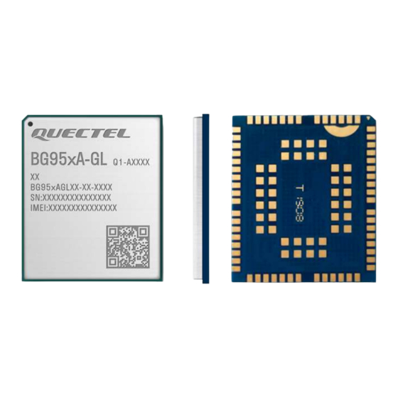
Figure 43: Top & Bottom Views of BG95xA-GL NOTE Images above are for illustrative purposes only and may differ from the actual module. For authentic appearance and label, please refer to the module received from Quectel. BG95xA-GL_Hardware_Design 93 / 102... -
Page 95: Storage, Manufacturing & Packaging
LPWA Module Series Storage, Manufacturing & Packaging 9.1. Storage Conditions The module is provided with vacuum-sealed packaging. MSL of the module is rated as 3. The storage requirements are shown below. 1. Recommended Storage Condition: the temperature should be 23 ±5 °C and the relative humidity should be 35–60 %. -
Page 96: Manufacturing And Soldering
LPWA Module Series NOTE 1. To avoid blistering, layer separation and other soldering issues, extended exposure of the module to the air is forbidden. 2. Take out the module from the package and put it on high-temperature-resistant fixtures before baking. All modules must be soldered to PCB within 24 hours of the baking, otherwise put them in the drying oven. -
Page 97: Packaging Specifications
Avoid using ultrasonic technology for module cleaning since it can damage crystals inside the module. Due to the SMT process complexity, please contact Quectel Technical Support in advance regarding any situation that you are not sure about, or any process (e.g., selective soldering, ultrasonic soldering) that is not mentioned in document [6]. -
Page 98: Plastic Reel
LPWA Module Series Figure 45: Carrier Tape Dimension Drawing Table 61: Carrier Tape Dimension Table (Unit: mm) 0.35 20.2 3.15 6.65 20.2 1.75 9.3.2. Plastic Reel Figure 46: Plastic Reel Dimension Drawing Table 62: Plastic Reel Dimension Table (Unit: mm) øD1 øD2 44.5... -
Page 99: Packing Process
LPWA Module Series 9.3.3. Packing Process Place the module onto the carrier tape and use the cover tape to cover them; then wind the heat-sealed carrier tape on the plastic reel and use the protective tape for protection. One plastic reel can load 250 modules. Place the packaged plastic reel, humidity indicator card and desiccant bag inside a vacuum bag, then vacuumize it. -
Page 100: Appendix References
LPWA Module Series Appendix References Table 63: Related Documents Document Name [1] Quectel_UMTS<E_EVB_User_Guide [2] Quectel_BG77xA-GL&BG95xA-GL_QCFG_AT_Commands_Manual [3] Quectel_BG77xA-GL&BG95xA-GL_AT_Commands_Manual [4] Quectel_BG770A-GL&BG95xA-GL_GNSS_Application_Note [5] Quectel_RF_Layout_Application_Note [6] Quectel_Module_Secondary_SMT_Application_Note [7] Quectel_BG950A-GL&BG951A-GL_TE-A_User_Guide Table 64: Terms and Abbreviations Abbreviation Description Analog to Digital Converter BeiDou Navigation Satellite System Balun Balanced to Unbalanced bit(s) per second... - Page 101 LPWA Module Series Discontinuous Reception EGSM Extended GSM (Global System for Mobile Communications) e-I-DRX Extended Idle Mode Discontinuous Reception Evolved Packet Core Electrostatic Discharge Evaluation Board Frequency Division Duplex FTP(S) FTP over SSL GNSS Global Navigation Satellite System GLONASS Global Navigation Satellite System (Russia) GPIO General-Purpose Input/Output Global Positioning System...
- Page 102 LPWA Module Series LwM2M Lightweight M2M Mobile Equipment Mobile Originated MQTT Message Queuing Telemetry Transport Moisture Sensitivity Levels Mobile Terminated NITZ Network Identity and Time Zone NMEA NMEA (National Marine Electronics Association) 0183 Interface Standard Power Amplifier Password Authentication Protocol Printed Circuit Board Protocol Data Unit PING...
- Page 103 LPWA Module Series Short Message Service Secure Sockets Layer Tracking Area Update Transmission Control Protocol TCXO Temperature Complementary Crystal Oscillator Transport Layer Security TTFF Time to First Fix Transmit UART Universal Asynchronous Receiver/Transmitter User Datagram Protocol Uplink User Equipment Unsolicited Result Code (U)SIM (Universal) Subscriber Identity Module Vmax...
- Page 104 The minimum distance between the user and/or any bystander and the radiating structure of the transmitter is 20cm. Hereby, We, Quectel Wireless Solutions Co., Ltd. declares that the radio equipment type BG953A-GL is in compliance with the Directive 2014/53/EU. The full text of the EU declaration of conformity is available at the following internet address: Building 5, Shanghai Business Park Phase III (Area B), No.1016 Tianlin Road, Minhang District,...
- Page 105 LPWA Module Series ❒ Catm LTE Band12:≤11.798dBi ❒ Catm LTE Band13:≤12.214dBi ❒ NB LTE Band2/25:≤11.000dBi ❒ NB LTE Band4/66:≤8.000dBi ❒ NB LTE Band5:≤12.541 dBi ❒ NB LTE Band12:≤11.798dBi ❒ NB LTE Band13:≤12.214dBi 5. This module must not transmit simultaneously with any other antenna or transmitter 6.
- Page 106 LPWA Module Series user manual must also contain clear instructions on how end users can find and/or access the module and the FCC ID. The final host / module combination may also need to be evaluated against the FCC Part 15B criteria for unintentional radiators in order to be properly authorized for operation as a Part 15 digital device.
- Page 107 LPWA Module Series Déclaration sur l'exposition aux rayonnements RF The EUT is a mobile device; maintain at least a 20 cm separation between the EUT and the user’s body and must not transmit simultaneously with any other antenna or transmitter. L'autre utilisé...
- Page 108 LPWA Module Series labeled to display the Innovation, Science and Economic Development Canada certification number for the module, preceded by the word “Contains” or similar wording expressing the same meaning, as follows: “Contains IC: 10224A-023BG953AGL” or “where: 10224A-023BG953AGL is the module’s certification number”.
- Page 109 LPWA Module Series BG95xA-GL_Hardware_Design 108 / 102...
Need help?
Do you have a question about the BG95 A-GL Series and is the answer not in the manual?
Questions and answers