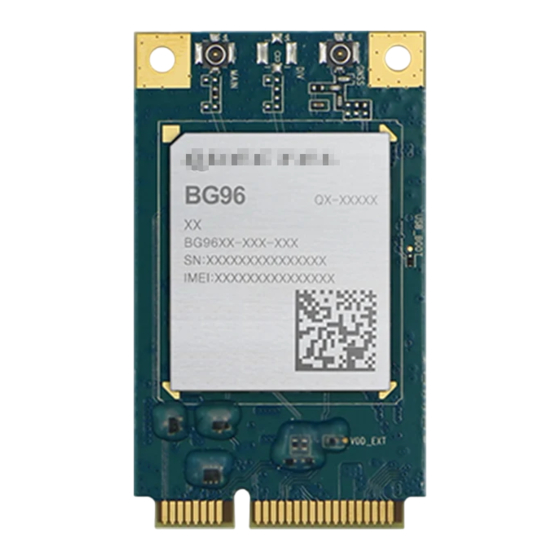
Quectel BG96 Mini PCIe Hardware Design
Hide thumbs
Also See for BG96 Mini PCIe:
- Developer's manual (90 pages) ,
- Manual (80 pages) ,
- Hardware design (79 pages)

Related Manuals for Quectel BG96 Mini PCIe


Summary of Contents for Quectel BG96 Mini PCIe
- Page 1 BG96 Mini PCIe Hardware Design LTE Module Series Rev. BG96_Mini_PCIe_Hardware_Design_V1.0 Date: 2018-09-12 Status: Preliminary www.quectel.com...
- Page 2 QUECTEL OFFERS THE INFORMATION AS A SERVICE TO ITS CUSTOMERS. THE INFORMATION PROVIDED IS BASED UPON CUSTOMERS’ REQUIREMENTS. QUECTEL MAKES EVERY EFFORT TO ENSURE THE QUALITY OF THE INFORMATION IT MAKES AVAILABLE. QUECTEL DOES NOT MAKE ANY WARRANTY AS TO THE INFORMATION CONTAINED HEREIN, AND DOES NOT ACCEPT ANY LIABILITY FOR ANY INJURY, LOSS OR DAMAGE OF ANY KIND INCURRED BY USE OF OR RELIANCE UPON THE INFORMATION.
-
Page 3: About The Document
LTE Module Series BG96 Mini PCIe Hardware Design About the Document History Revision Date Author Description Lyndon LIU/ 2018-09-12 Rex WANG/ Initial Hyman DING BG96_Mini_PCIe_Hardware_Design 2 / 40... -
Page 4: Table Of Contents
RF Characteristics ........................30 4.5. GNSS Receiver ........................32 4.6. ESD Characteristics ........................ 32 4.7. Current Consumption ......................33 Dimensions and Packaging ......................35 5.1. General Description ......................... 35 5.2. Mechanical Dimensions of BG96 Mini PCIe ................35 BG96_Mini_PCIe_Hardware_Design 3 / 40... - Page 5 LTE Module Series BG96 Mini PCIe Hardware Design 5.3. Standard Dimensions of Mini PCI Express ................36 5.4. Packaging Specification ......................37 Appendix A References ........................38 BG96_Mini_PCIe_Hardware_Design 4 / 40...
- Page 6 LTE Module Series BG96 Mini PCIe Hardware Design Table Index TABLE 1: SUPPORTED BANDS/GNSS FUNCTIONS OF BG96 MINI PCIE ............. 9 TABLE 2: KEY FEATURES OF BG96 MINI PCIE ..................... 10 TABLE 3: DEFINITION OF I/O PARAMETERS ....................14 TABLE 4: DESCRIPTION OF PINS ........................14 TABLE 5: DEFINITION OF VCC_3V3 AND GND PINS ..................
- Page 7 FIGURE 13: MECHANICALS OF U.FL-LP CONNECTORS ................28 FIGURE 14: SPACE FACTOR OF MATED CONNECTOR (UNIT: MM) ............28 FIGURE 15: MECHANICAL DIMENSIONS OF BG96 MINI PCIE ..............35 FIGURE 16: STANDARD DIMENSIONS OF MINI PCI EXPRESS ..............36 FIGURE 17: DIMENSIONS OF THE MINI PCI EXPRESS CONNECTOR (MOLEX 679100002) ....37...
-
Page 8: Introduction
This document can help customers to quickly understand module interface specifications, electrical and mechanical details as well as other related information of BG96 Mini PCIe module. To facilitate its application in different fields, relevant reference design is also provided for customers’ reference. -
Page 9: Safety Information
The following safety precautions must be observed during all phases of operation, such as usage, service or repair of any cellular terminal or mobile incorporating BG96 Mini PCIe module. Manufacturers of the cellular terminal should send the following safety information to users and operating personnel, and incorporate these guidelines into all manuals supplied with the product. -
Page 10: Product Concept
Product Concept 2.1. General Description BG96 Mini PCIe is an embedded IoT (LTE Cat M1, LTE Cat NB1 and EGPRS) wireless communication module. It provides data connectivity on LTE-FDD/LTE-TDD/GPRS/EGPRS networks and supports half-duplex operation with PCI Express Mini Card 1.2 standard interface. It also provides GNSS functionality to meet customers’... -
Page 11: Key Features
LTE Module Series BG96 Mini PCIe Hardware Design 2.2. Key Features The following table describes the detailed features of BG96 Mini PCIe module. Table 2: Key Features of BG96 Mini PCIe Feature Details Function Interface PCI Express Mini Card 1.2 Standard Interface Supply voltage: 3.0V~3.6V... - Page 12 Antenna Interface Include main antenna and GNSS antenna Gen8C Lite of Qualcomm GNSS Features Protocol: NMEA 0183 Compliant with 3GPP TS 27.007, 27.005 and Quectel enhanced AT AT Commands commands Size: (51.0± 0.15)mm × (30.0± 0.15)mm × (4.9± 0.2)mm Physical Characteristics Weight: approx.
-
Page 13: Functional Diagram
LTE Module Series BG96 Mini PCIe Hardware Design 2.3. Functional Diagram The following figure shows the block diagram of BG96 Mini PCIe. VBAT Boost Circuit Main Main Antenna Antenna Interface PCM&I2C BG96 UART Module GNSS GNSS (U)SIM Antenna Antenna Interface... -
Page 14: Application Interfaces
Control and indicator signals Antenna interfaces 3.1. Pin Assignment The following figure shows the pin assignment of BG96 Mini PCIe module. The top side contains BG96 module and antenna connectors. Pin Name Pin Name Pin No. Pin No. -
Page 15: Pin Description
LTE Module Series BG96 Mini PCIe Hardware Design 3.2. Pin Description The following tables show the pin definition and description of BG96 Mini PCIe on the 52-pin application. Table 3: Definition of I/O Parameters Type Description Bidirectional Digital Input Digital Output... - Page 16 LTE Module Series BG96 Mini PCIe Hardware Design Clock signal of (U)SIM UIM_CLK USIM_CLK card Connect to REFCLK+ UART_TX UART transmit data DTE’s RX. Reset signal of (U)SIM UIM_RESET USIM_RST card Mini card ground UIM_VPP RESERVED Reserved Output signal to wake up...
- Page 17 LTE Module Series BG96 Mini PCIe Hardware Design Mini card ground Mini card ground USB_D- USB_DM USB differential data (-) Mini card ground USB_D+ USB_DP USB differential data (+) 3.3Vaux VCC_3V3 3.3V DC supply Mini card ground 3.3Vaux VCC_3V3 3.3V DC supply...
-
Page 18: Power Supply
37, 40, 43, 50 The typical supply voltage of BG96 Mini PCIe is 3.3V. In the 2G network, the input peak current may reach 2.7A during the transmitting time. Therefore, the power supply must be able to provide enough current, and a bypass capacitor of no less than 470µF with low ESR should be used to prevent the voltage from... -
Page 19: U)Sim Interface
1.8V/3.0V (U)SIM card insertion detection BG96 Mini PCIe supports (U)SIM card hot-plug via the USIM_PRESENCE pin. The function supports low level and high level detections, and it is disabled by default. Please refer to document [2] about AT+QSIMDET command for details. - Page 20 LTE Module Series BG96 Mini PCIe Hardware Design If (U)SIM card detection function is not needed, please keep USIM_PRESENCE pin unconnected. A reference circuit for (U)SIM interface with a 6-pin (U)SIM card connector is illustrated in the following figure. 100nF...
-
Page 21: Usb Interface
USB differential data (+) BG96 Mini PCIe is compliant with USB 2.0 specification. It can only be used as a slave device. Meanwhile, it supports high speed (480Mbps) mode and full speed (12Mbps) mode. The USB interface is used for AT command communication, data transmission, GNSS NMEA output, software debugging, firmware upgrade. -
Page 22: Uart Interfaces
[2] for details. 3.7. PCM and I2C Interfaces* BG96 Mini PCIe provides one Pulse Code Modulation (PCM) digital interface and one I2C interface. The following table shows the pin definition of PCM and I2C interfaces that can be applied in audio codec... - Page 23 LTE Module Series BG96 Mini PCIe Hardware Design design. Table 8: Pin Definition of PCM and I2C Interfaces Pin No. Pin Name Power Domain Description PCM_CLK 1.8V PCM clock signal PCM_DOUT 1.8V PCM data output PCM_DIN 1.8V PCM data input PCM_SYNC 1.8V...
-
Page 24: Control And Indicator Signals
LTE Module Series BG96 Mini PCIe Hardware Design 3.8. Control and Indicator Signals The following table shows the pin definition of control and indicator signals. Table 9: Pin Definition of Control and Indicator Signals Pin No. Pin Name Power Domain... -
Page 25: W_Disable# Signal
BG96 Mini PCIe Hardware Design 3.8.3. W_DISABLE# Signal BG96 Mini PCIe module provides a W_DISABLE# signal to disable or enable the RF function (not include GNSS) by hardware method or software method. Hardware method can be controlled by W_DISABLE# signal, this function is disabled by default, and AT+QCFG="airplanecontrol", 1 can be used to enable this function. -
Page 26: Led_Wwan# Signal
3.8.5. LED_WWAN# Signal The LED_WWAN# signal of BG96 Mini PCIe is used to indicate the network status of the module, and can absorb the current up to 40mA. According to the following circuit, in order to reduce the current of the LED, a resistor must be placed in series with the LED. -
Page 27: Wake# Signal
URC return Figure 11: WAKE# Behavior 3.9. Antenna Interfaces BG96 Mini PCIe antenna interfaces include a main antenna interface and a GNSS antenna interface. 3.9.1. Antenna Requirements The following table shows the requirements on main antenna and GNSS antenna. BG96_Mini_PCIe_Hardware_Design... -
Page 28: Recommended Rf Connector For Antenna Installation
LTE Module Series BG96 Mini PCIe Hardware Design Table 14: Antenna Requirements Type Requirements Frequency range: 1559MHz~1609MHz Polarization: RHCP or linear VSWR: <2 (Typ.) GNSS Passive antenna gain: > 0dBi Active antenna noise figure: <1.5dB Active antenna gain: > 0dBi Active antenna embedded LNA gain: <17 dB... - Page 29 LTE Module Series BG96 Mini PCIe Hardware Design U.FL-LP serial connectors listed in the following figure can be used to match the U.FL-R-SMT. Figure 13: Mechanicals of U.FL-LP Connectors The following figure describes the space factor of mated connector. Figure 14: Space Factor of Mated Connector (Unit: mm) For more details, please visit http://www.hirose.com.
-
Page 30: Electrical, Reliability And Radio Characteristics
Thermal consideration 4.2. Power Supply Requirements The input voltage of BG96 Mini PCIe is 3.3V± 9%, as specified by PCI Express Mini CEM Specifications 1.2. The following table shows the power supply requirements of BG96 Mini PCIe. Table 15: Power Supply Requirements... -
Page 31: I/O Requirements
VCC_3V3 power domain. The maximum voltage value of V for PERST# signal and W_DISABLE# signal is 0.5V. 4.4. RF Characteristics The following tables show the conducted RF output power and receiving sensitivity of BG96 Mini PCIe module. BG96_Mini_PCIe_Hardware_Design 30 / 40... - Page 32 LTE Module Series BG96 Mini PCIe Hardware Design Table 18: BG96 Mini PCIe Conducted RF Output Power Frequency Max. Min. GSM850/EGSM900 33dBm± 2dB 5dBm± 5dB DCS1800/PCS1900 30dBm± 2dB 0dBm± 5dB GSM850/EGSM900 (8-PSK) 27dBm± 3dB 5dBm± 5dB DCS1800/PCS1900 (8-PSK) 26dBm± 3dB 0dBm±...
-
Page 33: Gnss Receiver
XTRA file contains predicted GPS and GLONASS satellites coordinates and clock biases valid for up to 7 days. It is best if XTRA file is downloaded every 1-2 days. Additionally, BG96 Mini PCIe can support standard NMEA-0183 protocol and output NMEA messages with 1Hz via USB NMEA interface. -
Page 34: Current Consumption
LTE Module Series BG96 Mini PCIe Hardware Design 4.7. Current Consumption The following tables describe the current consumption of BG96 Mini PCIe series module. Table 21: Current Consumption of BG96 Mini PCIe Parameter Description Conditions Typ. Unit AT+CFUN=0 (USB disconnected) - Page 35 DCS1800 (GNSS OFF) PCS1900 GSM850 GPRS GSM900 data transfer DCS1800 (GNSS OFF) PCS1900 Table 22: GNSS Current Consumption of BG96 Mini PCIe Parameter Description Conditions Typ. Unit Cold start @Passive Antenna Searching (AT+CFUN=0) Lost state @Passive Antenna VBAT...
-
Page 36: Dimensions And Packaging
This chapter mainly describes mechanical dimensions as well as packaging specification of BG96 Mini PCIe module. All dimensions are measured in mm. The tolerances for dimensions without tolerance values are ± 0.05mm. 5.2. Mechanical Dimensions of BG96 Mini PCIe Figure 15: Mechanical Dimensions of BG96 Mini PCIe BG96_Mini_PCIe_Hardware_Design 35 / 40... - Page 37 LTE Module Series BG96 Mini PCIe Hardware Design 5.3. Standard Dimensions of Mini PCI Express The following figure shows the standard dimensions of Mini PCI Express. Please refer to document [1] for detailed A and B. Figure 16: Standard Dimensions of Mini PCI Express...
- Page 38 [1]. The following figure takes the Molex 679100002 as an example. Figure 17: Dimensions of the Mini PCI Express Connector (Molex 679100002) 5.4. Packaging Specification BG96 Mini PCIe is packaged in a tray. Each tray contains 10 modules. The smallest package contains 100 modules. BG96_Mini_PCIe_Hardware_Design...
- Page 39 LTE Module Series BG96 Mini PCIe Hardware Design Appendix A References Table 23: Related Documents Document Name Remark PCI Express Mini Card Electromechanical Mini PCI Express specification Specification Revision 1.2 Quectel_BG96_AT_Commands_Manual BG96 AT commands manual Quectel_BG96_GNSS_AT_Commands_ BG96 GNSS AT commands manual...
- Page 40 LTE Module Series BG96 Mini PCIe Hardware Design GMSK Gaussian Minimum Shift Keying GNSS Global Navigation Satellite System Global Positioning System Global System for Mobile Communications kbps Kilo Bits Per Second Light Emitting Diode Long-Term Evolution Mbps Million Bits Per Second...
- Page 41 LTE Module Series BG96 Mini PCIe Hardware Design Universal Serial Bus (U)SIM (Universal) Subscriber Identification Module BG96_Mini_PCIe_Hardware_Design 40 / 40...
Need help?
Do you have a question about the BG96 Mini PCIe and is the answer not in the manual?
Questions and answers