
Related Manuals for Quectel BG77


Summary of Contents for Quectel BG77
- Page 1 BG77 Hardware Design LPWA Module Series Rev. BG77_Hardware_Design_V1.1 Date: 2019-10-08 Status: Preliminary www.quectel.com...
- Page 2 QUECTEL OFFERS THE INFORMATION AS A SERVICE TO ITS CUSTOMERS. THE INFORMATION PROVIDED IS BASED UPON CUSTOMERS’ REQUIREMENTS. QUECTEL MAKES EVERY EFFORT TO ENSURE THE QUALITY OF THE INFORMATION IT MAKES AVAILABLE. QUECTEL DOES NOT MAKE ANY WARRANTY AS TO THE INFORMATION CONTAINED HEREIN, AND DOES NOT ACCEPT ANY LIABILITY FOR ANY INJURY, LOSS OR DAMAGE OF ANY KIND INCURRED BY USE OF OR RELIANCE UPON THE INFORMATION.
- Page 3 LPWA Module Series BG77 Hardware Design About the Document History Revision Date Author Description Jake JIANG/ 2019-06-17 Initial Newgate HUA 1. Delete GNSS optional information. 2. Updated the power supply in Table 3. 3. Updated Pin Assignment in Figure 2.
-
Page 4: Table Of Contents
LPWA Module Series BG77 Hardware Design Contents About the Document ..........................2 Contents ..............................3 Table Index ............................... 5 Figure Index .............................. 7 Introduction ............................9 1.1. Safety Information ........................10 Product Concept ..........................11 2.1. General Description ........................ 11 2.2. - Page 5 LPWA Module Series BG77 Hardware Design 3.15. Behaviors of RI* ........................45 3.16. USB_BOOT Interface ......................45 3.17. ADC Interfaces ........................46 3.18. SPI Interface* ......................... 47 3.19. GPIO Interfaces* ........................48 3.20. GRFC Interfaces* ........................49 GNSS Receiver ..........................50 4.1.
-
Page 6: About The Document
LPWA Module Series BG77 Hardware Design Table Index TABLE 1: FREQUENCY BANDS AND GNSS TYPES OF BG77 MODULE ............. 11 TABLE 2: KEY FEATURES OF BG77 MODULE ....................12 TABLE 3: DEFINITION OF I/O PARAMETERS ....................17 TABLE 4: PIN DESCRIPTION ........................... 17 TABLE 5: OVERVIEW OF OPERATING MODES .................... -
Page 7: Contents
LPWA Module Series BG77 Hardware Design TABLE 42: RECOMMENDED THERMAL PROFILE PARAMETERS .............. 71 TABLE 43: REEL PACKAGING ........................73 TABLE 44: RELATED DOCUMENTS ....................... 74 TABLE 45: TERMS AND ABBREVIATIONS ..................... 74 BG77_Hardware_Design 6 / 76... - Page 8 LPWA Module Series BG77 Hardware Design Figure Index FIGURE 1: FUNCTIONAL DIAGRAM ....................... 14 FIGURE 2: PIN ASSIGNMENT (TOP VIEW) ....................16 FIGURE 3: SLEEP MODE APPLICATION VIA UART ..................28 FIGURE 4: STAR STRUCTURE OF THE POWER SUPPLY ................29 FIGURE 5: TURN ON THE MODULE USING DRIVING CIRCUIT ..............
- Page 9 LPWA Module Series BG77 Hardware Design FIGURE 39: REEL DIMENSIONS ........................73 BG77_Hardware_Design 8 / 76...
-
Page 10: Introduction
This document can help customers quickly understand the interface specifications, electrical and mechanical details, as well as other related information of BG77. To facilitate its application in different fields, reference design is also provided for customers’ reference. Associated with application notes and user guides, customers can use the module to design and set up mobile applications easily. -
Page 11: Safety Information
BG77. Manufacturers of the cellular terminal should send the following safety information to users and operating personnel, and incorporate these guidelines into all manuals supplied with the product. If not so, Quectel assumes no liability for customers’ failure to comply with these precautions. - Page 12 1.2 FCC Certification Requirements. According to the definition of mobile and fixed device is described in Part 2.1091(b), this device is a mobile device. And the following conditions must be met: 1. This Modular Approval is limited to OEM installation for mobile and fixed applications only.
- Page 13 ❒ NB LTE Band12/85:≤12.416dBi ❒ NB LTE Band13:≤11.734dBi ❒ BNLTE Band14:≤12.272 dBi ❒NB LTE Band71:≤11.447 dBi ❒NB LTE Band85:≤12.770 dBi 5. This module must not transmit simultaneously with any other antenna or transmitter 6. The host end product must include a user manual that clearly defines operating requirements and conditions that must be observed to ensure compliance with current FCC RF exposure guidelines.
- Page 14 users do not have straightforward commonly used methods for access to remove the module so that the FCC ID of the module is visible; then an additional permanent label referring to the enclosed module:“Contains Transmitter Module FCC ID: XMR201912BG77” or “Contains FCC ID: XMR201912BG77” must be used. The host OEM user manual must also contain clear instructions on how end users can find and/or access the module and the FCC ID.
-
Page 15: Product Concept
LTE Cat NB2 is backward compatible with LTE Cat NB1. “*” means under development. With a compact profile of 14.9mm × 12.9mm × 1.7mm, BG77 can meet almost all requirements for M2M applications such as smart metering, tracking system, security, wireless POS, etc. It is especially suitable for size and weight sensitive applications such as smart watch and other wearable devices. -
Page 16: Key Features
LPWA Module Series BG77 Hardware Design 2.2. Key Features The following table describes the detailed features of BG77 module. Table 2: Key Features of BG77 Module Features Details Supply voltage: 2.6V~4.8V Power Supply Typical supply voltage: 3.3V Transmitting Power Class 5 (21dBm+1/-3dB) for LTE-FDD bands ... -
Page 17: Functional Diagram
When the temperature returns to the normal operating temperature levels, the module will meet 3GPP specifications again. 2.3. Functional Diagram The following figure shows a block diagram of BG77 and illustrates the major functional parts. Power management ... -
Page 18: Evaluation Board
2. RESET_N is multiplexed from PWRKEY. 2.4. Evaluation Board In order to help customers to develop applications conveniently with BG77, Quectel supplies the evaluation board (EVB), USB to RS-232 converter cable, USB data cable, earphone, antenna and other peripherals to control or test the module. For more details, please refer to document [1]. -
Page 19: Application Interfaces
LPWA Module Series BG77 Hardware Design Application Interfaces BG77 is equipped with 94 LGA pads that can be connected to customers’ cellular application platforms. The following sub-chapters will provide detailed description of interfaces listed below: Power supply (U)SIM interface ... -
Page 20: Pin Assignment
LPWA Module Series BG77 Hardware Design 3.1. Pin Assignment The following figure shows the pin assignment of BG77. ANT_MAIN ANT_GNSS PON_TRIG 1 GPIO1 33 GPIO2 2 PCM_DIN 57 GPIO3 34 PCM_DOUT 3 PCM_CLK GRFC2 94 35 PCM_SYNC GRFC1 83 4 GNSS_RXD... -
Page 21: Pin Description
SPI_MOSI(pin40), NETLIGHT(pin79) and GPRC1(pin83) are BOOT_CONFIG pins, They should not be pulled up before startup. 3.2. Pin Description The following tables show the pin definition and description of BG77. Table 3: Definition of I/O Parameters Type Description Analog Input... - Page 22 LPWA Module Series BG77 Hardware Design Power supply for 1.8V output external GPIO’s power supply Vnorm=1.8V VDD_EXT pull-up circuits. for external max=50mA If unused, keep this circuit pin open. 22~25, 27, 28, 30, 31, 43, 47, 52~56, Ground 58, 66,...
- Page 23 LPWA Module Series BG77 Hardware Design max=1.8V USB_VBUS USB detection min=1.3V Compliant with USB USB differential USB_DP 2.0 standard data bus (+) specification. USB differential Require differential USB_DM data bus (-) impedance of 90Ω. Power for USB USB_VDDA_3P3 Vnorm=3.3V PHY circuit External LDO max=0.45V...
- Page 24 LPWA Module Series BG77 Hardware Design max=2.0V min=-0.3V 1.8V power domain. max=0.6V Receive data If unused, keep this min=1.2V pin open. max=2.0V 1.8V power domain. max=0.45V Transmit data If unused, keep this min=1.35V pin open. 1.8V power domain. max=0.45V Clear to send If unused, keep this min=1.35V...
- Page 25 LPWA Module Series BG77 Hardware Design PCM Interface* Pin Name Description DC Characteristics Comment 1.8V power domain. PCM clock max=0.45V If unused, keep this PCM_CLK output min=1.35V pin open. PCM frame 1.8V power domain. max=0.45V PCM_SYNC synchronization If unused, keep this min=1.35V...
- Page 26 LPWA Module Series BG77 Hardware Design BOOT_CONFIG. Do not pull it up SPI master-out before startup . max=0.45V SPI_MOSI slave-in 1.8V power domain. min=1.35V If unused, keep this pin open. min=-0.3V 1.8V power domain. SPI master-in max=0.6V SPI_MISO If unused, keep this slave-out min=1.2V...
- Page 27 LPWA Module Series BG77 Hardware Design to digital converter interface General purpose analog Voltage range: If unused, keep this ADC1 to digital 0.1V to 1.8V pin open. converter interface Other Interface Pins Pin Name Description DC Characteristics Comment 1.8V power domain.
-
Page 28: Operating Modes
7. ADC input voltage must not exceed 1.8V. 8. Keep all RESERVED pins and unused pins unconnected. 9. “*” means under development. 3.3. Operating Modes The table below briefly summarizes the various operating modes of BG77. BG77_Hardware_Design 24 / 76... -
Page 29: Power Saving
During this mode, the module can still receive paging message, SMS and TCP/UDP data from the network normally. Power Saving BG77 module may enter into Power Saving Mode to further reduce its power Mode consumption. PSM is similar to power-off, but the module remains registered on the (PSM) network and there is no need to re-attach or re-establish PDN connections. -
Page 30: Power Saving Mode (Psm)
3.4.2. Power Saving Mode (PSM) BG77 module can enter into PSM for reducing its power consumption. The mode is similar to power-off, but the module remains registered on the network and there is no need to re-attach or re-establish PDN connections. -
Page 31: Extended Idle Mode Drx (E-I-Drx)
Please refer to document [2] for details about AT+CEDRXS command. 3.4.4. Sleep Mode BG77 is able to reduce its current consumption to a lower value during the sleep mode. The following sub-chapters describe the power saving procedure of BG77 module. -
Page 32: Power Supply
BG77 Hardware Design Figure 3: Sleep Mode Application via UART When BG77 has URC to report, RI signal will wake up the host. Please refer to Chapter 3.14 for details about RI behavior. Driving the host DTR to low level will wake up the module. -
Page 33: Decrease Voltage Drop
BG77 Hardware Design 3.5.2. Decrease Voltage Drop The power supply range of BG77 is from 2.6V to 4.8V. Please make sure that the input voltage will never drop below 2.6V. To decrease voltage drop, a bypass capacitor of about 100µF with low ESR should be used, and a multi-layer ceramic chip capacitor (MLCC) array should also be reserved due to its low ESR. -
Page 34: Power On And Off Scenarios
Qualcomm chipset. When BG77 is in power off mode, it can be turned on to normal mode by driving the PWRKEY pin to a low level for a duration between 500ms and 1000ms. It is recommended to use an open drain/collector driver to control the PWRKEY. - Page 35 LPWA Module Series BG77 Hardware Design Figure 6: Turn on the Module Using Keystroke The power on timing is illustrated in the following figure. NOTE VBA T 500ms~1000ms PWRKEY VIL≤0.45V RESET_N Typ. 2.1s STATUS (DO) Typ. 2.55s Inactive Active Typ. 2.5s...
-
Page 36: Turn Off Module
LPWA Module Series BG77 Hardware Design 3.6.2. Turn off Module Either of the following methods can be used to turn off the module: Normal power down procedure: Turn off the module using the PWRKEY pin. Normal power down procedure: Turn off the module using AT+QPOWD command. - Page 37 LPWA Module Series BG77 Hardware Design The module can be reset by driving RESET_N low for a duration between 2s and 3.8s. Table 8: Pin Definition of RESET_N Pin Name Pin No. Description DC Characteristics Comment RESET_N Reset the module max=0.45V...
-
Page 38: Pon_Trig Interface
Please assure that there is no large capacitance on RESET_N pin. 3.8. PON_TRIG Interface BG77 provides one PON_TRIG pin which is used to wake up the module from PSM. When the pin detects a rising edge, the module will be woken up from PSM. -
Page 39: U)Sim Interface
Figure 12: Reference Circuit of PON_TRIG Circuit NOTE VDD_1V8 is provided by an external LDO. 3.9. (U)SIM Interface BG77 supports 1.8V (U)SIM card only. The (U)SIM interface circuitry meets ETSI and IMT-2000 requirements. Table 10: Pin Definition of (U)SIM Interface Pin Name Pin No. - Page 40 LPWA Module Series BG77 Hardware Design BG77 supports (U)SIM card hot-plug via USIM_DET. The function supports low level or high level detections, and is disabled by default. Please refer to document [2] about AT+QSIMDET command for details. The following figure shows a reference design of (U)SIM interface with an 8-pin (U)SIM card connector.
-
Page 41: Usb Interface
USIM_DET function is still under development. 3.10. USB Interface BG77 contains one integrated Universal Serial Bus (USB) interface which complies with the USB 2.0 specification and supports low-speed (1.5Mbps) and full-speed (12Mbps) modes. The USB interface is used for AT command communication, data transmission, software debugging and firmware upgrade. - Page 42 LPWA Module Series BG77 Hardware Design Power supply for USB PHY USB_VDDA_3P3 Vnorm=3.3V circuit EXT_PWR_EN External LDO enable of USB 1.8V power domain Ground For more details about USB 2.0 specification, please visit http://www.usb.org/home. The USB interface is recommended to be reserved for firmware upgrade in customers’ design. The following figures illustrate reference designs of USB PHY and USB interface.
-
Page 43: Uart Interfaces
Keep the ESD protection components as close to the USB connector as possible. NOTES 1. BG77 can only be used as a slave device. 2. The input voltage range of USB_VBUS is 1.3V~1.8V. 3.11. UART Interfaces The module provides three UART interfaces: Main UART, Debug UART and GNSS UART interfaces. - Page 44 LPWA Module Series BG77 Hardware Design Table 12: Pin Definition of Main UART Interface Pin Name Pin No. Description Comment Data terminal ready. 1.8V power domain Sleep mode control. Receive data 1.8V power domain Transmit data 1.8V power domain Clear to send 1.8V power domain...
- Page 45 LPWA Module Series BG77 Hardware Design Table 15: Logic Levels of Digital I/O Parameter Min. Max. Unit -0.3 0.45 1.35 The module provides 1.8V UART interfaces. A level translator should be used if customers’ application is equipped with a 3.3V UART interface. A level translator TXS0108EPWR provided by Texas Instruments is recommended.
-
Page 46: Pcm And I2C Interfaces
Transistor circuit solution is not suitable for applications with high baud rates exceeding 460Kbps. 3.12. PCM and I2C Interfaces* BG77 provides one Pulse Code Modulation (PCM) digital interface and one I2C interface. The following table shows the pin definition of the two interfaces which can be applied on audio codec design. -
Page 47: Network Status Indication
“*” means under development. 3.13. Network Status Indication BG77 provides one network status indication pin: NETLIGHT. The pin is used to drive a network status indication LED. The following tables describe the pin definition and logic level changes of NETLIGHT in different network activity status. -
Page 48: Status
NETLIGHT is a BOOT_CONFIG pin. It should not be pulled up before startup. 3.14. STATUS The STATUS pin is used to indicate the operation status of BG77 module. It will output high level when the module is powered on. The following table describes the pin definition of STATUS. -
Page 49: Behaviors Of Ri
LPWA Module Series BG77 Hardware Design Figure 21: Reference Circuit of STATUS 3.15. Behaviors of RI* AT+QCFG="risignaltype","physical" command can be used to configure RI behavior. No matter on which port URC is presented, URC will trigger the behavior of RI pin. -
Page 50: Adc Interfaces
LPWA Module Series BG77 Hardware Design BG77 provides a USB_BOOT pin. During development or factory production, USB_BOOT can force the module to boot from USB port for firmware upgrade. Table 21: Pin Definition of USB_BOOT Interface Pin Name Pin No. -
Page 51: Spi Interface
It is recommended to use resistor divider circuit for ADC application, and the divider resistor accuracy should be no less than 1%. 3.18. SPI Interface* BG77 module provides one SPI interface which support master/slave mode. Master mode: up to 50MHz ... -
Page 52: Gpio Interfaces
LPWA Module Series BG77 Hardware Design Table 24: Pin Definition of SPI Interface Pin Name Pin No. Description Comment BOOT_CONFIG. SPI_MOSI SPI master-out slave-in Do not pull it up before startup. 1.8V power domain SPI_MISO SPI master-in slave-out 1.8V power domain... -
Page 53: Grfc Interfaces
LPWA Module Series BG77 Hardware Design -0.3 0.45 1.35 NOTE “*” means under development. 3.20. GRFC Interfaces* The module provides two general RF control interfaces. Those can be used for control external antenna tuner. This function is under development. Table 27: Pin Definition of GRFC Interfaces Pin Name Pin No. -
Page 54: Gnss Receiver
BG77 supports standard NMEA-0183 protocol, and outputs NMEA sentences at 1Hz data update rate via USB interface by default. By default, BG77 GNSS engine is switched off. It has to be switched on via AT command. For more details about GNSS engine technology and configurations, please refer to document [3]. -
Page 55: Layout Guidelines
LPWA Module Series BG77 Hardware Design Autonomous Hot start @open sky XTRA enabled Accuracy Autonomous CEP-50 (GNSS) @open sky NOTES Tracking sensitivity: the lowest GNSS signal value at the antenna port on which the module can keep on positioning for 3 minutes. -
Page 56: Antenna Interfaces
LPWA Module Series BG77 Hardware Design Antenna Interfaces BG77 includes a main antenna interface and a GNSS antenna interface. The antenna ports have an impedance of 50Ω. 5.1. Main Antenna Interface 5.1.1. Pin Definition The pin definition of main antenna interface is shown below. -
Page 57: Reference Design Of Rf Antenna Interface
LPWA Module Series BG77 Hardware Design LTE-FDD B13 777~787 746~756 LTE-FDD B14 788~798 758~768 LTE-FDD B18 815~830 860~875 LTE-FDD B19 830~845 875~890 LTE-FDD B20 832~862 791~821 LTE-FDD B25 1850~1915 1930~1995 LTE-FDD B26* 814~849 859~894 LTE-FDD B27 807~824 852~869 LTE-FDD B28... -
Page 58: Reference Design Of Rf Layout
LPWA Module Series BG77 Hardware Design Figure 23: Reference Circuit of RF Antenna Interface 5.1.4. Reference Design of RF Layout For user’s PCB, the characteristic impedance of all RF traces should be controlled as 50Ω. The impedance of the RF traces is usually determined by the trace width (W), the materials’ dielectric constant, the distance between signal layer and reference ground (H), and the clearance between RF trace and ground (S). - Page 59 LPWA Module Series BG77 Hardware Design Figure 25: Coplanar Waveguide Line Design on a 2-layer PCB Figure 26: Coplanar Waveguide Line Design on a 4-layer PCB (Layer 3 as Reference Ground) Figure 27: Coplanar Waveguide Line Design on a 4-layer PCB (Layer 4 as Reference Ground)
-
Page 60: Gnss Antenna Interface
LPWA Module Series BG77 Hardware Design In order to ensure RF performance and reliability, the following principles should be complied with in RF layout design: Use impedance simulation tool to control the characteristic impedance of RF traces as 50Ω. -
Page 61: Antenna Installation
LPWA Module Series BG77 Hardware Design Figure 28: Reference Circuit of GNSS Antenna Interface NOTES An external LDO can be selected to supply power according to the active antenna requirement. If the module is designed with a passive antenna, then the VDD circuit is not needed. -
Page 62: Recommended Rf Connector For Antenna Installation
LPWA Module Series BG77 Hardware Design Cable Insertion Loss: < 1dB (LTE B5/B8/B12/B13/B14 /B18/B19/B20/B26*/B27 /B28/B71 / B85) Cable Insertion Loss: < 1.5dB (LTE B1/B2/B3/B4/B25/B66) NOTES It is recommended to use a passive GNSS antenna when LTE B13 or B14 is supported, as the use of active antenna may generate harmonics which will affect the GNSS performance. - Page 63 LPWA Module Series BG77 Hardware Design Figure 30: Mechanicals of U.FL-LP Connectors The following figure describes the space factor of mated connector. Figure 31: Space Factor of Mated Connector (Unit: mm) For more details, please visit http://www.hirose.com. BG77_Hardware_Design 59 / 76...
-
Page 64: Electrical, Reliability And Radio Characteristics
LPWA Module Series BG77 Hardware Design Electrical, Reliability and Radio Characteristics 6.1. Absolute Maximum Ratings Absolute maximum ratings for power supply and voltage on digital and analog pins of the module are listed in the following table. Table 35: Absolute Maximum Ratings Parameter Min. -
Page 65: Operation And Storage Temperatures
Pout might reduce in their value and exceed the specified tolerances. When the temperature returns to the normal operating temperature levels, the module will meet 3GPP specifications again. 6.4. Current Consumption The following table shows current consumption of BG77 module. Table 38: BG77 Current Consumption Parameter Description... - Page 66 LPWA Module Series BG77 Hardware Design DRX=1.28s DRX=1.28s Sleep State e-I-DRX=81.92s e-I-DRX=81.92s DRX=1.28s DRX=1.28s Idle State e-I-DRX=20.48s e-I-DRX=20.48s LTE-FDD B1 @TBDdBm LTE-FDD B2 @TBDdBm LTE-FDD B3 @TBDdBm LTE-FDD B4 @TBDdBm LTE-FDD B5 @TBDdBm LTE-FDD B8 @TBDdBm LTE-FDD B12 @TBDdBm LTE-FDD B13 @TBDdBm...
-
Page 67: Rf Output Power
LTE-FDD B19 @TBDdBm LTE-FDD B20 @TBDdBm LTE-FDD B25 @TBDdBm LTE-FDD B26 @TBDdBm LTE-FDD B28 @TBDdBm LTE-FDD B66 @TBDdBm LTE-FDD B71 @TBDdBm LTE-FDD B85 @TBDdBm 6.5. RF Output Power The following table shows the RF output power of BG77. BG77_Hardware_Design 63 / 76... -
Page 68: Rf Receiving Sensitivity
LTE-FDD B14 and B27 are supported by Cat M1 only. LTE-FDD B71 is supported by Cat NB2 only. “*” means under development. 6.6. RF Receiving Sensitivity The following table shows the conducted RF receiving sensitivity of BG77. Table 40: BG77 Conducted RF Receiving Sensitivity Sensitivity (dBm) Network Band... -
Page 69: Electrostatic Discharge
The following table shows the electrostatic discharge characteristics of BG77 module. Table 41: Electrostatic Discharge Characteristics (25ºC, 45% Relative Humidity) Tested Points... -
Page 70: Mechanical Dimensions
LPWA Module Series BG77 Hardware Design Mechanical Dimensions This chapter describes the mechanical dimensions of the module. All dimensions are measured in mm, and the tolerances for dimensions without tolerance values are ±0.05mm. 7.1. Mechanical Dimensions of the Module 12.90±0.15 1.7±0.2... - Page 71 LPWA Module Series BG77 Hardware Design 12.90±0.15 11.90 1.00 6.45 1.00 R0.35 Pin 1 0.65 0.85 1.30 0.85 0.65 0.65 1.15 R0.35 1.30 6.45 Figure 33: Module Bottom Dimensions (Bottom View) BG77_Hardware_Design 67 / 76...
-
Page 72: Recommended Footprint
LPWA Module Series BG77 Hardware Design 7.2. Recommended Footprint 12.90±0.15 11.90 1.00 6.45 1.00 R0.35 Pin 1 0.85 0.65 1.30 1.95 0.85 0.65 0.65 1.15 1.30 R0.35 6.45 Figure 34: Recommended Footprint (Top View) NOTES For easy maintenance of the module, please keep about 3mm between the module and other components on the host PCB. -
Page 73: Design Effect Drawings Of The Module
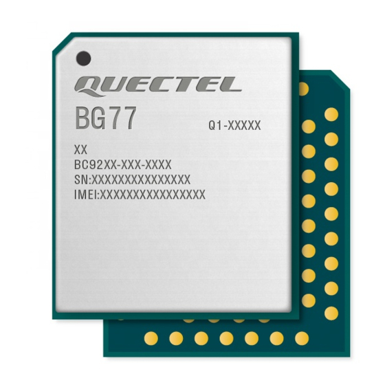
7.3. Design Effect Drawings of the Module Figure 35: Top View of the Module Figure 36: Bottom View of the Module NOTE These are renderings of BG77 module. For authentic appearance, please refer to the module that you receive from Quectel. BG77_Hardware_Design 69 / 76... -
Page 74: Storage, Manufacturing And Packaging
Packaging 8.1. Storage BG77 is stored in a vacuum-sealed bag. It is rated at MSL 3, and its storage restrictions are listed below. 1. Shelf life in the vacuum-sealed bag: 12 months at <40ºC/90%RH. 2. After the vacuum-sealed bag is opened, devices that will be subjected to reflow soldering or other high temperature processes must be: ... -
Page 75: Manufacturing And Soldering
LPWA Module Series BG77 Hardware Design 8.2. Manufacturing and Soldering Push the squeegee to apply the solder paste on the surface of stencil, thus making the paste fill the stencil openings and then penetrate to the PCB. The force on the squeegee should be adjusted properly so as to produce a clean stencil surface on a single pass. -
Page 76: Packaging
Max reflow cycle 8.3. Packaging BG77 is packaged in a vacuum-sealed bag which is ESD protected. The bag should not be opened until the devices are ready to be soldered onto the application. The following figures show the packaging details, measured in mm. - Page 77 LPWA Module Series BG77 Hardware Design Figure 39: Reel Dimensions Table 43: Reel Packaging Model Name MOQ for MP Minimum Package: 250pcs Minimum Package x 4=1000pcs BG77 BG77_Hardware_Design 73 / 76...
-
Page 78: Appendix A References
Table 44: Related Documents Document Name Remark Quectel_UMTS<E_EVB_User_Guide UMTS<E EVB User Guide Quectel_BG77_AT_Commands_Manual BG77 AT Commands Manual Quectel_BG77_GNSS_AT_Commands_Manual BG77 GNSS AT Commands Manual Quectel_RF_Layout_Application_Note RF Layout Application Note Quectel_Module_Secondary_SMT_User_Guide Module Secondary SMT User Guide Table 45: Terms and Abbreviations Abbreviation Description... - Page 79 LPWA Module Series BG77 Hardware Design Electrostatic Discharge Frequency Division Duplex Full Rate GMSK Gaussian Minimum Shift Keying Global System for Mobile Communications Home Subscriber Server Input/Output Inorm Normal Current Light Emitting Diode Low Noise Amplifier Long Term Evolution Mobile Originated...
- Page 80 LPWA Module Series BG77 Hardware Design Transmitting Direction Uplink User Equipment Unsolicited Result Code (U)SIM (Universal) Subscriber Identity Module Vmax Maximum Voltage Value Vnorm Normal Voltage Value Vmin Minimum Voltage Value Maximum Input High Level Voltage Value Minimum Input High Level Voltage Value...
Need help?
Do you have a question about the BG77 and is the answer not in the manual?
Questions and answers