Quectel BG96 Series Hardware Design
Lte module
Hide thumbs
Also See for BG96 Series:
- Developer's manual (90 pages) ,
- Manual (80 pages) ,
- Application note (53 pages)

Related Manuals for Quectel BG96 Series


Summary of Contents for Quectel BG96 Series
- Page 1 BG96 Hardware Design LTE Module Series Rev. BG96_Hardware_Design_V1.2 Date: 2017-12-22 Status: Released www.quectel.com...
- Page 2 QUECTEL OFFERS THE INFORMATION AS A SERVICE TO ITS CUSTOMERS. THE INFORMATION PROVIDED IS BASED UPON CUSTOMERS’ REQUIREMENTS. QUECTEL MAKES EVERY EFFORT TO ENSURE THE QUALITY OF THE INFORMATION IT MAKES AVAILABLE. QUECTEL DOES NOT MAKE ANY WARRANTY AS TO THE INFORMATION CONTAINED HEREIN, AND DOES NOT ACCEPT ANY LIABILITY FOR ANY INJURY, LOSS OR DAMAGE OF ANY KIND INCURRED BY USE OF OR RELIANCE UPON THE INFORMATION.
-
Page 3: About The Document
LTE Module Series BG96 Hardware Design About the Document History Revision Date Author Description Lyndon LIU/ 2017-08-04 Initial Daryl DU 1. Modified GSM features in Table 2. 2. Added a note for e-I-DRX in Chapter 3.3. 2017-08-31 Daryl DU 3. Elaborated the description of e-I-DRX in Chapter 3.4.3. -
Page 4: Table Of Contents
LTE Module Series BG96 Hardware Design Contents About the Document ........................... 2 Contents ............................... 3 Table Index ..............................5 Figure Index ..............................7 Introduction ............................8 1.1. Safety Information........................9 Product Concept ..........................10 2.1. General Description ......................... 10 2.2. Key Features ........................... - Page 5 LTE Module Series BG96 Hardware Design GNSS Receiver ........................... 45 4.1. General Description ......................... 45 4.2. GNSS Performance ......................... 45 4.3. Layout Guidelines ........................46 Antenna Interfaces ..........................47 5.1. Main Antenna Interface ......................47 5.1.1. Pin Definition ........................47 5.1.2.
- Page 6 LTE Module Series BG96 Hardware Design Table Index TABLE 1: FREQUENCY BANDS OF BG96 MODULE ..................10 TABLE 2: KEY FEATURES OF BG96 MODULE ....................11 TABLE 3: DEFINITION OF I/O PARAMETERS ....................17 TABLE 4: PIN DESCRIPTION ........................... 17 TABLE 5: OVERVIEW OF OPERATING MODES .....................
- Page 7 LTE Module Series BG96 Hardware Design TABLE 42: EDGE MODULATION AND CODING SCHEMES ................78 BG96_Hardware_Design 6 / 78...
- Page 8 LTE Module Series BG96 Hardware Design Figure Index FIGURE 1: FUNCTIONAL DIAGRAM ....................... 13 FIGURE 2: PIN ASSIGNMENT (TOP VIEW)..................... 16 FIGURE 3: SLEEP MODE APPLICATION VIA UART ..................26 FIGURE 4: STAR STRUCTURE OF THE POWER SUPPLY................28 FIGURE 5: TURN ON THE MODULE USING DRIVING CIRCUIT ..............29 FIGURE 6: TURN ON THE MODULE USING KEYSTROKE ................
-
Page 9: Introduction
LTE Module Series BG96 Hardware Design Introduction This document defines BG96 module and describes its air interface and hardware interfaces which are connected with customers’ applications. This document can help customers quickly understand the interface specifications, electrical and mechanical details, as well as other related information of BG96. To facilitate its application in different fields, reference design is also provided for customers’... -
Page 10: Safety Information
BG96. Manufacturers of the cellular terminal should send the following safety information to users and operating personnel, and incorporate these guidelines into all manuals supplied with the product. If not so, Quectel assumes no liability for customers’ failure to comply with these precautions. -
Page 11: Product Concept
LTE Module Series BG96 Hardware Design Product Concept 2.1. General Description BG96 is an embedded IoT (LTE Cat M1, LTE Cat NB1 and EGPRS) wireless communication module. It provides data connectivity on LTE-TDD/LTE-FDD/GPRS/EDGE networks, and supports half-duplex operation in LTE networks. It also provides GNSS and voice functionality to meet customers’... -
Page 12: Key Features
LTE Module Series BG96 Hardware Design 2.2. Key Features The following table describes the detailed features of BG96 module. Table 2: Key Features of BG96 Module Features Details Supply voltage: 3.3V~4.3V Power Supply Typical supply voltage: 3.8V Class 3 (23dBm± 2dB) for LTE-FDD bands Class 3 (23dBm±... - Page 13 Used for outputting GNSS data or NEMA sentences 115200bps baud rate 3GPP TS 27.007 and 3GPP TS 27.005 AT commands, as well as AT Commands Quectel enhanced AT commands Network Indication One NETLIGHT pin for network connectivity status indication Including main antenna (ANT_MAIN) and GNSS antenna (ANT_GNSS)
-
Page 14: Functional Diagram
LTE Module Series BG96 Hardware Design Within extended temperature range, the module remains the ability to establish and maintain a voice, SMS, data transmission, emergency call, etc. There is no unrecoverable malfunction. There are also no effects on radio spectrum and no harm to radio network. Only one or more parameters like might reduce in their value and exceed the specified tolerances. -
Page 15: Evaluation Board
“*” means under development. 2.4. Evaluation Board In order to help customers develop applications conveniently with BG96, Quectel supplies the evaluation board (EVB), USB to RS-232 converter cable, USB data cable, earphone, antenna and other peripherals to control or test the module. For more details, please refer to document [1]. -
Page 16: Application Interfaces
LTE Module Series BG96 Hardware Design Application Interfaces BG96 is equipped with 102 LGA pads that can be connected to customers’ cellular application platforms. The following sub-chapters will provide detailed description of interfaces listed below: Power supply (U)SIM interface ... -
Page 17: Pin Assignment
LTE Module Series BG96 Hardware Design 3.1. Pin Assignment The following figure shows the pin assignment of BG96. PSM_IND* ANT_GNSS ADC1* USIM_GND PCM_CLK* USIM_CLK PCM_SYNC* USIM_DATA PCM_IN* USIM_RST PCM_OUT* USIM_VDD GPIO64 USB_VBUS USIM_PRESENCE USB_DP I2C_SDA* I2C_SCL* USB_DM USB_BOOT RESERVED RESERVED RESERVED RESERVED PWRKEY... -
Page 18: Pin Description
LTE Module Series BG96 Hardware Design NOTES Keep all RESERVED pins and unused pins unconnected. GND pads should be connected to ground in the design. PWRKEY output voltage is 0.8V because of the diode drop in the Qualcomm chipset. “*” means under development. 3.2. - Page 19 LTE Module Series BG96 Hardware Design Provide 1.8V for Vnorm=1.8V Power supply for external VDD_EXT GPIO’s pull up circuits. external circuit max=50mA 3, 31, 48, 50, 54, 55, 58, 59, 61, 62, 67~74, Ground 79~82, 89~91, 100~102 Turn on/off Pin Name Pin No.
- Page 20 LTE Module Series BG96 Hardware Design (U)SIM Interface Pin Name Pin No. Description Comment Characteristics min=-0.3V (U)SIM card 1.8V power domain. USIM_ max=0.6V insertion If unused, keep this pin PRESENCE min=1.2V detection open. max=2.0V For 1.8V (U)SIM: Vmax=1.9V Vmin=1.7V Either 1.8V or 3.0V is Power supply USIM_VDD supported by the module...
- Page 21 LTE Module Series BG96 Hardware Design UART1 Interface Pin Name Pin No. Description Comment Characteristics min=-0.3V Data terminal 1.8V power domain. max=0.6V ready(sleep If unused, keep this pin min=1.2V mode control) open. max=2.0V min=-0.3V 1.8V power domain. max=0.6V Receive data If unused, keep this pin min=1.2V open.
- Page 22 LTE Module Series BG96 Hardware Design 1.8V power domain. max=0.45V UART3_TXD Transmit data If unused, keep this pin min=1.35V open. min=-0.3V 1.8V power domain. max=0.6V UART3_RXD Receive data If unused, keep this pin min=1.2V open. max=2.0V PCM* Interface Pin Name Pin No.
- Page 23 LTE Module Series BG96 Hardware Design Other Pins Pin Name Pin No. Description Comment Characteristics 1.8V power domain. Power saving max=0.45V PSM_IND If unused, keep this pin mode indicator min=1.35V open. 1.8V power domain. Pull-up by default. min=-0.3V In low voltage level, the Airplane mode max=0.6V W_DISABLE#*...
-
Page 24: Operating Modes
LTE Module Series BG96 Hardware Design General purpose analog Voltage range: If unused, keep this pin ADC0* to digital 0.3V to 1.8V open. converter interface RESERVED Pins Pin Name Pin No. Description Comment Characteristics 11~14, 16, 25, 51, 56, 57, 63, 65, Keep these pins RESERVED Reserved... -
Page 25: Power Saving
LTE Module Series BG96 Hardware Design Airplane AT+CFUN command or W_DISABLE#* pin can set the module into airplane mode. In this Mode case, RF function will be invalid. Minimum AT+CFUN command can set the module into a minimum functionality mode without Functionality removing the power supply. -
Page 26: Power Saving Mode (Psm)
LTE Module Series BG96 Hardware Design NOTES Airplane mode control via W_DISABLE# is disabled in firmware by default. It can be enabled by AT+QCFG=“airplanecontrol” command. The command is still under development. The execution of AT+CFUN command will not affect GNSS function. “*”... -
Page 27: Sleep Mode
LTE Module Series BG96 Hardware Design value in the subscription data from the HSS, may also provide different values of the e-I-DRX parameters than what was requested by the UE. If the EPC accepts the use of e-I-DRX, the UE applies e-I-DRX based on the received e-I-DRX parameters. -
Page 28: Power Supply
LTE Module Series BG96 Hardware Design Driving the host DTR to low level will wake up the module. When BG96 has URC to report, RI signal will wake up the host. Please refer to Chapter 3.14 for details about RI behavior. ... -
Page 29: Monitor The Power Supply
LTE Module Series BG96 Hardware Design To decrease voltage drop, a bypass capacitor of about 100µF with low ESR should be used, and a multi-layer ceramic chip capacitor (MLCC) array should also be reserved due to its low ESR. It is recommended to use three ceramic capacitors (100nF, 33pF, 10pF) for composing the MLCC array, and place these capacitors close to VBAT pins. - Page 30 LTE Module Series BG96 Hardware Design Table 7: Pin Definition of PWRKEY Pin Name Pin No. Description DC Characteristics Comment The output voltage is max=2.1V 0.8V because of the PWRKEY Turn on/off the module min=1.3V diode drop in the max=0.5V Qualcomm chipset.
-
Page 31: Turn Off Module
LTE Module Series BG96 Hardware Design The turn on scenario is illustrated in the following figure. NOTE VBAT ≥100ms ≥1.3V ≤0.5V PWRKEY RESET_N ≥ 4.8s STATUS (DO) ≥ 4.2s Inactive Active ≥ 4.9s URAT Inactive Active Figure 7: Timing of Turning on Module NOTE Make sure that VBAT is stable before pulling down PWRKEY pin. -
Page 32: Turn Off Module Using At Command
LTE Module Series BG96 Hardware Design The power-down scenario is illustrated in the following figure. VBAT ≥ 650ms ≥ 2s PWRKEY STATUS Module Power-down procedure RUNNING Status Figure 8: Timing of Turning off Module 3.6.2.2. Turn off Module Using AT Command It is also a safe way to use AT+QPOWD command to turn off the module, which is similar to turning off the module via PWRKEY pin. - Page 33 LTE Module Series BG96 Hardware Design The recommended circuit is similar to the PWRKEY control circuit. An open drain/collector driver or button can be used to control the RESET_N. RESET_N 150~460ms 4.7K Reset pulse Figure 9: Reference Circuit of RESET_N by Using Driving Circuit RESET_N Close to S2 Figure 10: Reference Circuit of RESET_N by Using Button...
-
Page 34: U)Sim Interface
LTE Module Series BG96 Hardware Design NOTES Use RESET_N only when turning off the module by AT+QPOWD command and PWRKEY pin both failed. Ensure that there is no large capacitance on PWRKEY and RESET_N pins. 3.8. (U)SIM Interface The (U)SIM interface circuitry meets ETSI and IMT-2000 requirements. Both 1.8V and 3.0V (U)SIM cards are supported. - Page 35 LTE Module Series BG96 Hardware Design The following figure shows a reference design of (U)SIM interface with an 8-pin (U)SIM card connector. VDD_EXT USIM_VDD 100nF (U)SIM Card Connector USIM_GND USIM_VDD USIM_RST Module USIM_CLK USIM_PRESENCE USIM_DATA 33pF 33pF 33pF Figure 12: Reference Circuit of (U)SIM Interface with an 8-Pin (U)SIM Card Connector If (U)SIM card detection function is not needed, please keep USIM_PRESENCE unconnected.
-
Page 36: Usb Interface
LTE Module Series BG96 Hardware Design Keep placement of (U)SIM card connector as close to the module as possible. Keep the trace length as less than 200mm as possible. Keep (U)SIM card signals away from RF and VBAT traces. ... -
Page 37: Uart Interfaces
LTE Module Series BG96 Hardware Design Test Points Minimize these stubs Module NM_0R NM_0R ESD Array USB_VBUS USB_DM USB_DM USB_DP USB_DP Close to Module Figure 14: Reference Circuit of USB Application In order to ensure signal integrity of USB data lines, components R1, R2, R3 and R4 must be placed close to the module, and also should be placed close to each other. - Page 38 LTE Module Series BG96 Hardware Design UART1 interface supports 9600, 19200, 38400, 57600, 115200, 230400, 460800 and 921600 baud rates, and the default is 115200bps. It is used for data transmission and AT command communication. UART2 interface supports 115200bps baud rate. It is used for module debugging and log output. ...
- Page 39 LTE Module Series BG96 Hardware Design The logic levels are described in the following table. Table 14: Logic Levels of Digital I/O Parameter Min. Max. Unit -0.3 0.45 1.35 The module provides 1.8V UART interface. A level translator should be used if customers’ application is equipped with a 3.3V UART interface.
-
Page 40: Pcm* And I2C* Interfaces
LTE Module Series BG96 Hardware Design 4.7K VDD_EXT VDD_EXT Module MCU/ARM VDD_EXT VCC_MCU 4.7K GPIO EINT GPIO Figure 16: Reference Circuit with Transistor Circuit NOTE Transistor circuit solution is not suitable for applications with high baud rates exceeding 460Kbps. 3.11. PCM* and I2C* Interfaces BG96 provides one Pulse Code Modulation (PCM*) digital interface and one I2C* interface. -
Page 41: Network Status Indication
LTE Module Series BG96 Hardware Design The following figure shows a reference design of PCM* and I2C* interfaces with an external codec IC. MICBIAS PCM_CLK BCLK PCM_SYNC WCLK PCM_IN PCM_OUT LOUTP I2C_SCL I2C_SDA LOUTN Module Codec 1.8V Figure 17: Reference Circuit of PCM Application with Audio Codec NOTE “*”... -
Page 42: Status
LTE Module Series BG96 Hardware Design Table 17: Working State of NETLIGHT Pin Name Logic Level Changes Network Status Flicker slowly (200ms High/1800ms Low) Network searching Flicker slowly (1800ms High/200ms Low) Idle NETLIGHT Flicker quickly (125ms High/125ms Low) Data transfer is ongoing Always high Voice calling A reference circuit is shown in the following figure. -
Page 43: Behaviors Of Ri
LTE Module Series BG96 Hardware Design The following figure shows a reference circuit of STATUS. VBAT Module 2.2K 4.7K STATUS Figure 19: Reference Circuit of STATUS 3.14. Behaviors of RI AT+QCFG=“risignaltype”,“physical” command can be used to configure RI behavior. No matter on which port URC is presented, URC will trigger the behavior of RI pin. NOTE URC can be outputted from UART port, USB AT port and USB modem port, through configuration via AT+QURCCFG command. -
Page 44: Usb_Boot Interface
LTE Module Series BG96 Hardware Design 3.15. USB_BOOT Interface BG96 provides a USB_BOOT pin. During development or factory production, USB_BOOT can force the module to boot from USB port for firmware upgrade. Table 20: Pin Definition of USB_BOOT Interface Pin Name Pin No. - Page 45 LTE Module Series BG96 Hardware Design In order to improve the accuracy of ADC voltage values, the trace of ADC should be surrounded by ground. Table 21: Pin Definition of ADC Interfaces Pin Name Pin No. Description ADC0 General purpose analog to digital converter interface ADC1 General purpose analog to digital converter interface The following table describes the characteristics of ADC interfaces.
-
Page 46: Gnss Receiver
LTE Module Series BG96 Hardware Design GNSS Receiver 4.1. General Description BG96 includes a fully integrated global navigation satellite system solution that supports Gen8C-Lite of Qualcomm (GPS, GLONASS, BeiDou/Compass, Galileo and QZSS). BG96 supports standard NMEA-0183 protocol, and outputs NMEA sentences at 1Hz data update rate via USB interface by default. -
Page 47: Layout Guidelines
LTE Module Series BG96 Hardware Design @open sky XTRA* enabled Accuracy Autonomous CEP-50 < 2.5 (GNSS) @open sky NOTES Tracking sensitivity: the lowest GNSS signal value at the antenna port on which the module can keep on positioning for 3 minutes. Reacquisition sensitivity: the lowest GNSS signal value at the antenna port on which the module can fix position again within 3 minutes after loss of lock. -
Page 48: Antenna Interfaces
LTE Module Series BG96 Hardware Design Antenna Interfaces BG96 includes a main antenna interface and a GNSS antenna interface. The antenna ports have an impedance of 50Ω. 5.1. Main Antenna Interface 5.1.1. Pin Definition The pin definition of main antenna interface is shown below. Table 24: Pin Definition of Main Antenna Interface Pin Name Pin No. -
Page 49: Reference Design Of Rf Antenna Interface
LTE Module Series BG96 Hardware Design 777~787 746~757 815~829.9 860~874.9 830~844.9 875~889.9 832~862 791~821 814~848.9 859~893.9 703~748 758~803 1880~1920 1880~1920 5.1.3. Reference Design of RF Antenna Interface A reference design of main antenna pad is shown as below. A π-type matching circuit should be reserved for better RF performance, and the π-type matching components (R1/C1/C2) should be placed as close to the antenna as... - Page 50 LTE Module Series BG96 Hardware Design Figure 22: Microstrip Line Design on a 2-layer PCB Figure 23: Coplanar Waveguide Line Design on a 2-layer PCB Figure 24: Coplanar Waveguide Line Design on a 4-layer PCB (Layer 3 as Reference Ground) BG96_Hardware_Design 49 / 78...
-
Page 51: Gnss Antenna Interface
LTE Module Series BG96 Hardware Design Figure 25: Coplanar Waveguide Line Design on a 4-layer PCB (Layer 4 as Reference Ground) In order to ensure RF performance and reliability, the following principles should be complied with in RF layout design: ... - Page 52 LTE Module Series BG96 Hardware Design Table 27: GNSS Frequency Type Frequency Unit GPS/Galileo/QZSS 1575.42± 1.023 GLONASS 1597.5~1605.8 BeiDou 1561.098± 2.046 A reference design of GNSS antenna interface is shown as below. GNSS 0.1uF Antenna Module 47nH 100pF ANT_GNSS Figure 26: Reference Circuit of GNSS Antenna Interface NOTES An external LDO can be selected to supply power according to the active antenna requirement.
-
Page 53: Antenna Installation
LTE Module Series BG96 Hardware Design 5.3. Antenna Installation 5.3.1. Antenna Requirements The following table shows the requirements on main antenna and GNSS antenna. Table 28: Antenna Requirements Antenna Type Requirements VSWR: ≤ 2 Gain (dBi): 1 Max Input Power (W): 50 Input Impedance (Ω): 50 Polarization Type: Vertical LTE/GSM Antenna... - Page 54 LTE Module Series BG96 Hardware Design Figure 27: Dimensions of the U.FL-R-SMT Connector (Unit: mm) U.FL-LP serial connectors listed in the following figure can be used to match the U.FL-R-SMT. Figure 28: Mechanicals of U.FL-LP Connectors BG96_Hardware_Design 53 / 78...
- Page 55 LTE Module Series BG96 Hardware Design The following figure describes the space factor of mated connector. Figure 29: Space Factor of Mated Connector (Unit: mm) For more details, please visit http://www.hirose.com. BG96_Hardware_Design 54 / 78...
-
Page 56: Electrical, Reliability And Radio Characteristics
LTE Module Series BG96 Hardware Design Electrical, Reliability and Radio Characteristics 6.1. Absolute Maximum Ratings Absolute maximum ratings for power supply and voltage on digital and analog pins of the module are listed in the following table. Table 29: Absolute Maximum Ratings Parameter Min. -
Page 57: Operation And Storage Temperatures
LTE Module Series BG96 Hardware Design Parameter Description Conditions Min. Typ. Max. Unit USB_VBUS USB detection 5.25 6.3. Operation and Storage Temperatures The operation and storage temperatures of the module are listed in the following table. Table 31: Operation and Storage Temperatures Parameter Min. - Page 58 LTE Module Series BG96 Hardware Design Table 32: BG96 Current Consumption Parameter Description Conditions Typ. Unit OFF State Power down Power Saving Mode @Real Network Quiescent AT+CFUN=0 Current DRX=1.28s @Real LTE Cat M1 Network DRX=1.28s @Real LTE Cat NB1 Network Sleep State e-I-DRX=20.48s @Real LTE Cat M1 Network e-I-DRX=20.48s @Real LTE Cat NB1 Network...
- Page 59 LTE Module Series BG96 Hardware Design LTE-FDD B20 @23.46dBm LTE-FDD B26 @23.34dBm LTE-FDD B28 @23.67dBm LTE-TDD B39 @TBD LTE-FDD B1 @23.5dBm LTE-FDD B2 @23.3dBm LTE-FDD B3 @23.5dBm LTE-FDD B4 @23.6dBm LTE-FDD B5 @23.5dBm LTE-FDD B8 @23.1dBm LTE Cat NB1 data transfer LTE-FDD B12 @23.6dBm (GNSS OFF) LTE-FDD B13 @23.3dBm...
- Page 60 LTE Module Series BG96 Hardware Design DCS1800 4UL1DL @29.95dBm DCS1800 3UL2DL @30.15dBm DCS1800 2UL3DL @30.34dBm DCS1800 1UL4DL @30.54dBm PCS1900 4UL1DL @29.58dBm PCS1900 3UL2DL @29.72dBm PCS1900 2UL3DL @29.91dBm PCS1900 1UL4DL @30.11dBm GSM850 4UL1DL @26.35dBm GSM850 3UL2DL @26.47dBm GSM850 2UL3DL @26.69dBm GSM850 1UL4DL @26.88dBm GSM900 4UL1DL @26.05dBm GSM900 3UL2DL @26.46dBm GSM900 2UL3DL @26.33dBm...
-
Page 61: Rf Output Power
LTE Module Series BG96 Hardware Design NOTES Typical value with USB and UART disconnected. Sleep state with UART connected and USB disconnected. The module can enter into sleep state through executing AT+QSCLK=1 command via UART interface and then controlling the module’s DTR pin. -
Page 62: Rf Receiving Sensitivity
LTE Module Series BG96 Hardware Design 6.6. RF Receiving Sensitivity The following table shows the conducted RF receiving sensitivity of BG96 module. Table 35: BG96 Conducted RF Receiving Sensitivity Sensitivity (dBm) Network Band Primary Diversity Cat M1/3GPP Cat NB1 /3GPP LTE-FDD B1 -107.0/-102.7 -112.5/-107.5... -
Page 63: Electrostatic Discharge
LTE Module Series BG96 Hardware Design NOTE LTE Cat NB1 receiving sensitivity without repetitions. 6.7. Electrostatic Discharge The module is not protected against electrostatics discharge (ESD) in general. Consequently, it is subject to ESD handling precautions that typically apply to ESD sensitive components. Proper ESD handling and packaging procedures must be applied throughout the processing, handling and operation of any application that incorporates the module. -
Page 64: Mechanical Dimensions
LTE Module Series BG96 Hardware Design Mechanical Dimensions This chapter describes the mechanical dimensions of the module. All dimensions are measured in mm, and the tolerances for dimensions without tolerance values are ± 0.05mm. 7.1. Mechanical Dimensions of the Module 22.50±0.15 2.3±0.2 Figure 30: Module Top and Side Dimensions... - Page 65 LTE Module Series BG96 Hardware Design Figure 31: Module Bottom Dimensions (Bottom View) BG96_Hardware_Design 64 / 78...
-
Page 66: Recommended Footprint And Stencil Design
LTE Module Series BG96 Hardware Design 7.2. Recommended Footprint and Stencil Design Figure 32: Recommended Footprint (Top View) BG96_Hardware_Design 65 / 78... - Page 67 LTE Module Series BG96 Hardware Design Figure 33: Recommended Stencil Design (Top View) NOTES For easy maintenance of the module, please keep about 3mm between the module and other components on the host PCB. All reserved pins must be kept open. The thickness of stencil should be stepped-up to 0.18mm.
-
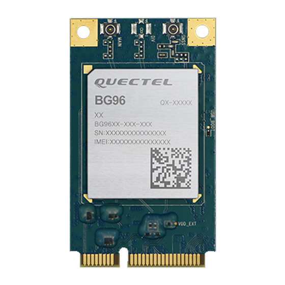
Page 68: Design Effect Drawings Of The Module
Figure 34: Top View of the Module Figure 35: Bottom View of the Module NOTE These are design effect drawings of BG96 module. For more accurate pictures, please refer to the module that you get from Quectel. BG96_Hardware_Design 67 / 78... -
Page 69: Storage, Manufacturing And Packaging
LTE Module Series BG96 Hardware Design Storage, Manufacturing and Packaging 8.1. Storage BG96 is stored in a vacuum-sealed bag. The storage restrictions are shown as below. 1. Shelf life in the vacuum-sealed bag: 12 months at <40º C/90%RH. 2. After the vacuum-sealed bag is opened, devices that will be subjected to reflow soldering or other high temperature processes must be: ... -
Page 70: Manufacturing And Soldering
LTE Module Series BG96 Hardware Design 8.2. Manufacturing and Soldering Push the squeegee to apply the solder paste on the surface of stencil, thus making the paste fill the stencil openings and then penetrate to the PCB. The force on the squeegee should be adjusted properly so as to produce a clean stencil surface on a single pass. - Page 71 LTE Module Series BG96 Hardware Design The reel is 330mm in diameter and each reel contains 250 modules. The following figures show the packaging details, measured in mm. Figure 37: Tape Dimensions 48.5 Cover tape Direction of feed +0.20 44.5 -0.00 Figure 38: Reel Dimensions BG96_Hardware_Design...
- Page 72 LTE Module Series BG96 Hardware Design Table 37: Reel Packaging Model Name MOQ for MP Minimum Package: 250pcs Minimum Package x 4=1000pcs Size: 370mm × 350mm × 56mm Size: 380mm × 250mm × 365mm BG96 250pcs N.W: 0.78kg N.W: 3.1kg G.W: 1.46kg G.W: 6.45kg BG96_Hardware_Design...
-
Page 73: Appendix A References
LTE Module Series BG96 Hardware Design Appendix A References Table 38: Related Documents Document Name Remark Quectel_UMTS<E_EVB_User_Guide UMTS<E EVB User Guide Quectel_BG96_AT_Commands_Manual BG96 AT Commands Manual Quectel_BG96_GNSS_AT_Commands_Manual BG96 GNSS AT Commands Manual Quectel_RF_Layout_Application_Note RF Layout Application Note Quectel_Module_Secondary_SMT_User_Guide Module Secondary SMT User Guide Table 39: Terms and Abbreviations Abbreviation Description... - Page 74 LTE Module Series BG96 Hardware Design Frequency Division Duplex Full Rate GMSK Gaussian Minimum Shift Keying Global System for Mobile Communications Home Subscriber Server Input/Output Inorm Normal Current Light Emitting Diode Low Noise Amplifier Long Term Evolution Mobile Originated Mobile Station (GSM engine) Mobile Terminated Password Authentication Protocol Printed Circuit Board...
- Page 75 LTE Module Series BG96 Hardware Design Unsolicited Result Code (U)SIM (Universal) Subscriber Identity Module Vmax Maximum Voltage Value Vnorm Normal Voltage Value Vmin Minimum Voltage Value Maximum Input High Level Voltage Value Minimum Input High Level Voltage Value Maximum Input Low Level Voltage Value Minimum Input Low Level Voltage Value Absolute Maximum Input Voltage Value Absolute Minimum Input Voltage Value...
-
Page 76: Appendix B Gprs Coding Schemes
LTE Module Series BG96 Hardware Design Appendix B GPRS Coding Schemes Table 40: Description of Different Coding Schemes Scheme CS-1 CS-2 CS-3 CS-4 Code Rate Pre-coded USF Radio Block excl.USF and BCS Tail Coded Bits Punctured Bits 9.05 13.4 15.6 21.4 Data Rate Kb/s BG96_Hardware_Design... -
Page 77: Appendix C Gprs Multi-Slot Classes
LTE Module Series BG96 Hardware Design Appendix C GPRS Multi-slot Classes Twenty-nine classes of GPRS multi-slot modes are defined for MS in GPRS specification. Multi-slot classes are product dependent, and determine the maximum achievable data rates in both the uplink and downlink directions. - Page 78 LTE Module Series BG96 Hardware Design BG96_Hardware_Design 77 / 78...
-
Page 79: Appendix D Edge Modulation And Coding Schemes
LTE Module Series BG96 Hardware Design Appendix D EDGE Modulation and Coding Schemes Table 42: EDGE Modulation and Coding Schemes Coding Modulation Coding Family 1 Timeslot 2 Timeslot 4 Timeslot Schemes CS-1: GMSK 9.05kbps 18.1kbps 36.2kbps CS-2: GMSK 13.4kbps 26.8kbps 53.6kbps CS-3: GMSK...
Need help?
Do you have a question about the BG96 Series and is the answer not in the manual?
Questions and answers